UNIVERSITI TEKNIKAL MALAYSIA MELAKA
UMTS ANTENNA DESIGN
This report submitted in accordance with requirement of the Universiti Teknikal Malaysia Melaka (UTeM) for the Bachelor Degree of Electronic Engineering
Technology (Telecommunications) with Honours.
by
NORSHARIMIE BINTI MAT ADAM B071110114
900422035048
UNIVERSITI TEKNIKAL MALAYSIA MELAKA
BORANG PENGESAHAN STATUS LAPORAN PROJEK SARJANA MUDA
TAJUK: UMTS Antenna Design
SESI PENGAJIAN: 2014/15 Semester 2
Saya NORSHARIMIE BINTI MAT ADAM
mengaku membenarkan Laporan PSM ini disimpan di Perpustakaan Universiti Teknikal Malaysia Melaka (UTeM) dengan syarat-syarat kegunaan seperti berikut:
1. Laporan PSM adalah hak milik Universiti Teknikal Malaysia Melaka dan penulis. 2. Perpustakaan Universiti Teknikal Malaysia Melaka dibenarkan membuat salinan
untuk tujuan pengajian sahaja dengan izin penulis.
3. Perpustakaan dibenarkan membuat salinan laporan PSM ini sebagai bahan pertukaran antara institusi pengajian tinggi.
4. **Sila tandakan ( )
SULIT
TERHAD
TIDAK TERHAD
(Mengandungi maklumat yang berdarjah keselamatan atau kepentingan Malaysia sebagaimana yang termaktub dalam AKTA RAHSIA RASMI 1972)
(Mengandungi maklumat TERHAD yang telah ditentukan oleh organisasi/badan di mana penyelidikan dijalankan)
Alamat Tetap:
Tarikh: ________________________
Disahkan oleh:
Cop Rasmi:
Tarikh: _______________________
DECLARATION
I hereby, declared this report entitled “UMTS Antenna Design” is the results of my own research except as cited in references.
Signature : ……….
Author’s Name : ………
ii
APPROVAL
This report is submitted to the Faculty of Engineering Technology of UTeM as a partial fulfillment of the requirements for the degree of Bachelor of Engineering Technology (Telecommunications) with Honours. The member of the supervisory is as follow:
iii
ABSTRAK
iv
ABSTRACT
v
DEDICATION
Special dedications to:
My beloved mother, father, siblings and friends who encouraged and inspired me
throughout my journey of education.
My Supervisor,Mr. Win Adiyansyah Indra
vi
ACKNOWLEDGEMENT
In the name of Allah, the Most Beneficent and Most Merciful.
First of all, I am thankful to Allah the Almighty, and the Merciful for giving me strength and the ability to complete this project.
I am sincerely grateful to my supervisor, Mr. Win Adiyansyah Indra for his guidance, constructive ideas, invaluable support and encouragement to this final year project. His helpful ideas and willingness to spend his time to help me has made this project possible. This work would have been impossible without his precious support and encouragement.
I would also like to thank Mr. Mohd Saad Bin Hamid and Mr. Nadzrie Bin Mohamood for evaluating my project progress, and for their encouragement and crucial suggestions to this project.
My deep gratitude goes to my loving parents, who watched me from a distance while I worked towards my degree. Without their love, affection and encouragement this work would not have been possible. I also like to take this opportunity to express my appreciation to my siblings for their constant support, comfort, advice and patience they have bestowed upon me.
vii
TABLE OF CONTENT
CHAPTER TITLE PAGE
TITLE PAGE i
DECLARATION ii
APPROVAL iii
ABSTRAK iv
ABSTRACT v
DEDICATION vi
ACKNOWLEDGEMENT vii
TABLE OF CONTENTS viii
LIST OF TABLES xii
LIST OF FIGURES xiii
LIST OF ABBREVIATIONS, SYMBOL AND xv
NOMENCLATURE LIST OF APPENDICES xvi
CHAPTER I INTRODUCTION 1.1 Introduction 1
1.2 Objectives 2
1.3 Problem Statement 2
1.4 Project Scopes 3
1.5 Thesis outline 3
CHAPTER II LITERATURE REVIEW 2.1 Introduction 4
2.2 Basic characteristic of Microstrip 5
viii
2.3.1 Radiation pattern 7
2.3.2 Return loss (RL) 8
2.3.3 Voltage standing wave ratio (VSWR) 10
2.3.4 Gain 10
2.3.5 Bandwidth 11
2.4 Substrate Materials 12
2.4.1 Effective Dielectric Constant 12
2.4.2 Characteristic Impedance 13
2.5 Fundamentals of Transmission Line 13
2.6 Description of Previous Methods 14
2.6.1 Microstrip antenna design for UMTS 14
Handset 2.6.2 Design of printed dipole antenna and 16
Its applications in UMTS mobile Communication Networks CHAPTER III METHODOLOGY 3.1 Introduction 18
3.2 Project planning 19
3.3 Design procedures 21
3.3.1 Antenna design by mathematical 23
formulation 3.3.2 Signal Feed 25
3.4 CST Microwave Studio design procedure 25
3.4.1 Model the substrate 27
3.4.2 Model the ground plane 28
3.4.3 Model the Dipole 30
3.4.4 Port for Coaxial Feeding 31
3.4.5 Common solver setting 32
ix
3.4.5.2 Boundary Conditions 33
3.4.5.3 Define Farfield Monitor 34
3.5 Antenna Fabrication 35
3.6 Antenna measurement 38
CHAPTER IV RESULTS AND ANALYSIS 4.1 Introduction 40
4.2 Simulation Results 40
4.2.1 Design Structure 41
4.2.2 Return loss 44
4.2.3 Input impedance 45
4.2.4 Bandwidth 46
4.2.5 VSWR 46
4.2.6 Radiation pattern and axial ratio 47
4.3 Measurement Result 49
4.3.1 Return loss 49
4.3.2 Input impedance 50
4.3.3 VSWR 51
4.4 Comparison between Simulation and 52
Measurement Results of Folded Dipole Antenna 4.4.1 Return loss 52
4.4.2 Input impedance 53
4.4.3 VSWR 54
CHAPTER V CONCLUSION AND RECOMMENDATION 5.1 Introduction 56
5.2 Conclusion 56
x
REFERENCES 58
xi
LIST OF TABLES
xii
LIST OF FIGURES
2.1 Basic Operation of Transmit and Received Antenna 5
2.2 Basic structure of microstrip patch antenna 6
2.3 Different shapes of patch 6
2.4 The radiation pattern of antenna 8
2.5 Return Loss Graph 9
2.6 The design of microstrip patch antenna 15
2.8 Measurement result 16
2.9 The design of antenna 17
2.10 Simulation and measurement result 17
3.1 Flow chart of the project 20
3.2 The unfolded dipole antenna 21
3.3 The design of folded dipole antenna 22
3.4 SMA connector- socket SMA panel. 25
3.5 CST microwave studio project 26
3.6 Antenna template 26
3.7 Substrate brick creation 27
3.8 Substrate 28
3.9 Pick face on the back of FR4 substrate 28
3.10 Extrude tool. 29
3.11 Ground plane. 29
3.12 Partial design of folded dipole antenna. 30
3.13 Full design of folded dipole antenna. 31
3.14 Port for coaxial feeding 32
3.15 Frequency range 33
3.16 Boundary condition menu 33
3.17 Folded dipole antenna with boundary conditions. 34
3.18 Far-field monitor 34
xiii
3.20 Glue 39
3.21 Layout of unfolded antenna using Autocad 36
3.22 Layout of unfolded antenna 36
3.23 Folded dipole antenna 37
3.24 Figure of making the antenna by putting some glue. 37
3.25 Complete folded dipole antenna 38
3.26 Rohde & Schwarz ZVB 14 vector network analyzer. 38
3.27 Measurement of folded dipole antenna. 39
4.1 The unfolded dipole antenna. 41
4.2 The design of folded dipole antenna. 41
4.3 Fabrication of folded dipole antenna 42
4.4 Return loss of simulated folded dipole antenna 44
4.5 Simulated input impedance of folded dipole antenna. 45
4.6 Simulated bandwidth 46
4.7 Simulated VSWR 47
4.8 Far-field directivity of folded dipole antenna. 48
4.9 Axial ratio of folded dipole antenna (phi = 0). 48
4.10 Measured VSWR 49
4.11 Measured input impedance of folded dipole antenna 50
4.12 Measured VSWR 51
[image:15.595.111.497.66.525.2]xiv
LIST OF ABBREVIATIONS, SYMBOLS AND
NOMENCLATURE
UMTS Universal Mobile Telecommunication System
PCB Printed Circuit Board
CST Computer Software Technology
MWS Microwave Studio
EM Electromagnetic
S11 Return Loss
dB Decibels
BW Bandwidth
VSWR Voltage Standing Wave Ratio
HPBW Half Power Bandwidth
SMA Sub Miniature A
FR4 Fire retardant 4
RL Return Loss
Γ reflection coefficient
Zo characteristic impedance
Hz hertz
K kilo
h height
l length
w width
ε r dielectric constant of the substrate c speed of light 3x 10⁻⁸ m/s
xv
LIST OF APPENDICES
A Gantt chart
1
1.1 Objective
Over the recent years, the need to expand the bandwidth of antennas in mobile handheld devices follows from the ever-increasing data rates, and hence spectrum requirements, of mobile devices. The implementation of antenna design causing minimised coupling with the human head and hand, hence minimised SAR would be attractive to many consumers, thus increasing the market acceptance of devices using such antennas. A good candidate is a balanced antenna [1]. An antenna with symmetrical structure that is fed with balanced currents to make it electrically symmetrical is said to be a balanced antenna. Dipoles and loops are the most commonly encountered balanced antennas [2, 3].
Compact UMTS antenna is designed in this work to cover the frequency bands for Universal Mobile Telecommunication System (UMTS). UMTS is a third generation mobile cellular technology for network based on the GSM standard. The UMTS antenna is proposed due to its application for the third generation and ideal for the users in the modern world. Once it is implemented, the users can be constantly attached to the internet as they travel and have the same set of capabilities no matter where they travel to.
With the recent advances of telecommunication, the need for small antennas has greatly increased. Various techniques have been proposed to develop a size of a folded dipole antenna. This geometry of the proposed antenna is four folded edge and slotted rectangular antenna. In this case, it is called folded dipole antenna. The
INTRODUCTION
2 dimension of this antenna has the value of less than 30 × 30 mm. In addition, it has a 15% bandwidth with return loss of less than -10 dB from 1885 MHz to 2250 MHz. All the criteria must be achieved while developing the antenna.
1.2 Objective
The objectives for this project are:
1.2.1 To investigate a balance antenna for mobile handset application with enhanced bandwidth performance, which cover UMTS frequency bands. 1.2.2 To achive the criteria that was given to this project such as bandwidth and
return loss.
1.2.3 To design and fabricated compact UMTS antenna.
1.3 Problem Statement
In the past, various techniques have been proposed to develop a size of folded dipole antenna for UMTS application. However, most of the design is quite big and consume a lot of space inside the handset mobile user. In this work, a compact UMTS antenna is proposed with small size and good overall performance.
1.4 Project Scope
The scope of this project is to design an antenna that fulfills the desired frequency of UMTS which is can operate at frequency from 1885 MHz to 2250 MHz.
(a) Hardware
3 (b) Software
The software that is used to design this antenna is Computer Simulation Technology design microwave (CST 2011). It is used to design an antenna with suitable parameters to get the simulation of return loss versus frequency.
1.5 Thesis Outline
4
2.1 Introduction
An antenna is capable of radiating and capturing radio waves. It is used to interface transmission line to free space, free space in transmission line, or both [4]. An antenna can be any shape or size. A list of some common types of antennas is wire, aperture, microstrip, reflector, and arrays. Each antenna configuration has a radiation pattern and design parameters, in addition to their benefits and drawbacks. In this section we will describe common antenna types and their benefits and drawbacks.
The transmission line couples energy from a transmitter to an antenna or vice versa. Then, the antenna couples the energy from the transmission lines into the earth atmosphere and from the earth atmosphere to the transmission line. At the transmit end of a wireless communication system, the antenna converts electrical energy travelling along the transmission line into an electromagnetic waves that are emitted into space. While at the receiving end of a wireless communication system, the antenna converts electromagnetic waves in the space into electrical energy on a transmission line.
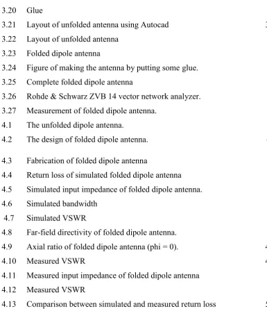
The transmitter can be modelled as a Thevenin source consisting of voltage generator and series impedance which delivers a transmit power to the transmit antenna. The transmit antenna radiates a spherical wave which, at large distances, approximates a plane wave, at least over a localized area. The receive antenna intercepts a portion of the propagating wave and delivers a receive power. Figure 2.1 shows the basic operation of transmitting and received antenna.
LITERATURE REVIEW
5 Figure 2.1: Basic operation of transmit and received antenna
2.2 Basic Characteristic of Microstrip
6
[image:23.595.153.525.86.274.2]
Figure 2.2: Basic structure of microstrip patch antenna
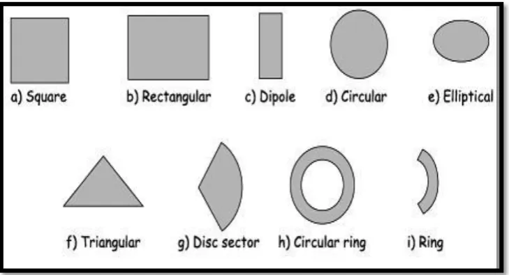
The bottom layer of the dielectric is completely covered with copper and it is known as the ground plane. The topside of the dielectric is partly metalized or patched whereby antenna or circuit pattern can be printed. Figure 2.3 shows the different shapes, which the radiating patch element may take the form. The attractive radiation characteristics, especially low cross polarization radiation make the square, rectangular, dipole and circular shapes the simple and common in terms of analysis and fabrication.
[image:23.595.153.518.510.707.2]7
2.3 Antenna Properties
Although there are many antenna types and geometries, the most important parameters that characterize all antenna designs need to be considered. These parameters provide information about the properties of an antenna.
2.3.1 Radiation Pattern
The radiation pattern is defined as the graphical representation of power radiated or received by an antenna in a function of the angular position and radial distance from the antenna [5]. It is a representation of how the signal propagates from the antenna. In other words, the radiation pattern is a graphical representation of the relative field strength transmitted from or received by the antenna. Radiation patterns of an antenna are usually measured in the far field region in most of the cases where the distributions of radiated power are independent of the distance. It can be determined in the 2-D or 3-D plot.