1
Study of the beam profile and position instability of a post-accelerated
pseudospark-sourced electron beam
J. Zhao
1,2,3,a), H. Yin
3, L. Zhang
3, G. Shu
3, W. He
3, A. D. R. Phelps
3, A. W. Cross
3,
L. Pang
1,2and Q. Zhang
1,21
State Key Laboratory of Electrical Insulation and Power Equipment, Xi’an, 710049, China
2
High Voltage Division, School of Electrical Engineering, Xi’an Jiaotong University, Xi’an, 710049, China
3
Department of Physics, SUPA, University of Strathclyde, Glasgow, G4 0NG, Scotland, United Kingdom
A pseudospark-sourced electron beam is a promising candidate for driving a THz millimeter wave radiation source. However, the physics governing the electron beam density profile and the beam center deviation from the axis of the structure, which may be caused by the randomness in the pseudospark discharge process, remains still unclear especially for the high energy component of the pseudospark-sourced electron beam which is usually non-mono-energetic. It is essential to study the electron beam density profile and the beam center position distribution for optimizing the pseudospark discharge
configuration. In this paper, images of some single-shot electron beam pulses have been captured using a 50 μm thickness
stopping copper foil and a phosphor screen coated with P47 scintillator to study the electron beam density profile and the beam center position distribution of the high energy component of the electron beam. The experiments have been carried out on two pseudospark discharge configurations with two different size hollow cathode cavities. The influence of the cathode aperture of each configuration has also been studied according to the beam images. Experimental results show that the beam profile of the high energy component has a Lorentzian distribution and is much smaller than the axial aperture size with the beam centers dispersing within a certain range around the axis of the discharge structure. The pseudospark-sourced electron beam with the larger hollow cathode cavity shows smaller full width at half maximum (FWHM) radius and a more concentrated beam center distribution.
I. INTRODUCTION
The pseudospark discharge is an axially symmetric transient, low pressure gas discharge which occurs in a special hollow cathode configuration and operates on the left-hand branch of the Paschen curve. An intense electron beam will be generated during the discharge process and can be extracted from the discharge chamber through a central
axial aperture in the electrodes1-4. The pseudospark-sourced
electron beam has attractive applications in many fields
such as free electron masers5, extreme-ultraviolet6 and soft
x-ray7 radiation sources, especially in driving THz radiation
sources8-11 due to its high current density and brightness.
As a plasma cathode operating in a low pressure gas, a pseudospark-based intense electron beam source is different from a hot thermionic cathode, or a photocathode operating at room temperature in vacuum. The current density profile and the beam center distribution of the pseudospark-sourced electron beam could be influenced by the discharge process. Due to the high operating frequency, the dimensions of a typical THz beam-wave interaction structure are down to the submillimeter range and the driving current density
needs to be hundreds of amperes per square centimeter9-11.
Deviation of the electron beam profile and its center position over the submillimeter range could significantly degrade the performance of the radiation source and the physics governing the beam profile and the center position
of a pseudospark-sourced electron beam is still unclear. So it is essential to study the distribution of the beam current density and the beam center variation to optimize the design of future beam-wave interaction structures.
Depending on the discharge process, the electron energy of the pseudospark-sourced electron beam disperses in a certain range up to the applied voltage during the
discharge12,13. Only the high energy component of the
electron beam can interact with the electromagnetic wave to generate high frequency radiation.
Christiansen1 found the high energy part of the electron
beam had a mean diameter of 60 μm measured through
sputtering a hole in a copper plate by 104 pseudospark
discharges with an applied voltage of 70 kV and using electrode apertures of 1.0 mm diameter. Benker observed a
300 μm crater on an aluminum target formed by the electron
beam with an applied voltage of 50 kV2. Destler found the
diameter of the high energy 200keV part of the electron beam was in the range of 0.2 to 1.4 mm using a copper
stopping foil and heat sensitive polycarbonate sheet14. Zhu
found electron beam damage patterns on acid-sensitive discoloring film and copper foil and then observed the damage holes had diameters in the 0.3 mm to 0.5 mm
range15. Dewald16 studied the electron beam induced plasma
light intensity profiles in the radial direction through fast shutter photographs and found the beam diameter to be about 1 mm.
The measurements detailed above were based on the
bombardment of the electron beam by over 103 to 104 times
a)Author to whom correspondence should be addressed. Electronic
generated in
2
and the result of each single shot may be blurred by an accumulative effect. In this paper, the electron beam density profile and beam center position distribution of the high energy component of a post-accelerated pseudospark discharge electron beam source configuration have been studied through the beam images captured by a scintillator
screen after a 50 μm stopping copper foil. The electron
beam density profile and center position of each shot were obtained from the beam image of a single shot. Beam profiles and center distributions of different discharge configurations are also analyzed using the experimental results.
II. Experimental configuration
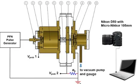
The experiments have been carried out on a post-accelerated pseudospark discharge electron beam source, as presented in figure 1. The pulse generator is a 15-stage pulse forming network (PFN) Blumlein structure with capacitance of ~0.76 nF and inductance of ~186 nH in each stage.
There is a very small discharge gap of 0.2 mm between a 2 mm through hole at the end of the hollow cathode chamber and a 1.6 mm rod-like head of the trigger electrode, which serves as a trigger discharge gap for the pseudospark discharge.
Two sizes of the hollow cathode chamber were used in the experiments. The diameters and depths of the hollow cathode cavities were 26 mm and 12 mm for the smaller chamber (abbreviated as SC in the following text) and 48 mm and 46 mm for the bigger chamber (abbreviated as LC in the following text), respectively. The axial apertures of the anode and the grounded flange are all of diameter 3 mm
while the diameter of the cathode aperture is systematically varied by using the three values of 2, 3 and 4 mm for both the SC and LC configurations to study the influence of the discharge process on the electron beam. The pseudospark
discharge gap separation of 16 mm17 was used to get a
relatively high beam current and the post-acceleration gap
separation was 6 mm. A 400 Ω high voltage resistor
connected the anode and the grounded flange, which ensured the pulsed voltage, was applied on the trigger gap, the pseudospark gap and the post-acceleration gap
successively. Two high voltage probes, Vprob1 and Vprob2
(1000:1 Tektronix P6015A), were used to measure the voltage pulses on the cathode and the anode respectively, as presented in figure 1. When the phosphor screen was replaced by a Faraday cup, the beam current was measured simultaneously.
When the PFN high voltage pulse was applied between the trigger electrode and the grounded flange, most of the voltage dropped on the trigger gap first before the breakdown of the pseudospark discharge gap because of the small capacitance of the trigger discharge gap. The first breakdown definitely occurs across this small gap due to the extremely high electric field strength when a sufficiently high voltage is applied.
The operating voltage of the post-accelerated pseudospark-discharge electron beam source is ~38 kV with the charging voltage of ~19 kV. A phosphor screen coated with P47 scintillator powder with peak emission wavelength at 400 nm was used for capturing the image of the electron beam. The decay time of P47 scintillator are about 80 ns and the response time is well under the decay time. A stopping
copper foil with thickness of 50 μm was placed in front of
the screen to attenuate the high energy component of the electron beam to sufficient low current to avoid the ablation of the scintillator. The stopping foil also blocks the low energy electrons, soft bremsstrahlung x-rays
the foil by the electron beam and other radiation generated by the discharge which can also stimulate the scintillator.
The total energy of the bremsstrahlung x-ray is estimated to
be at least three orders of magnitude lower than the energy of the electron beam after the stopping copper foil. This ensured the scintillator was stimulated mainly by the high energy component of the electron beam.
The image on the phosphor screen was recorded by a Nikon D50 digital camera with lens of Nikon AF-S Micro Nikkor 105mm F/2.8. The CCD of the camera is sensitive to light with wavelength as low as 380 nm and the lens can transmit the visible and part of the UV lights, which well match the wavelength of the P47 scintillator emission. The shutter time of the camera is set to one second while a single shot of the pseudospark discharge triggered during this
period after the shutter was opened. The experimental
[image:2.612.58.288.55.196.2]device and the camera were set up in a dark, radiation-shielded room and the camera was controlled by a computer
FIG. 1. Post-acceleration and beam image capture of the pseudospark-sourced electron beam. trigger electrode ○1, trigger
discharge gap ○2 , pseudospark cathode ○3 , hollow cathode
cavity ○4, cathode aperture ○5, pseudospark discharge gap ○6,
pseudospark anode with aperture ○7, post-acceleration gap ○8,
grounded flange with output aperture○9, Phosphor screen with
3
located outside of the room through a USB cable with image data acquired through a cable after the shutter was closed, so that the beam image of each single shot could be individually captured and stored in the computer.
III. Experimental results and discussions
A. Typical discharge waveforms and electron beam image
In both the SC and LC configuration, the typical waveforms of the discharge voltage and the beam current are shown in figure 2. When a high voltage pulse was applied to the structure, the trigger gap breaks down first and the voltage on the cathode begins to rise sharply. The
voltage on the anode, that is the post acceleration voltage of the electron beam, and the electron beam out of the aperture on the grounded flange begin to rise when the pseudospark discharge gap (cathode-anode gap) breakdown starts at ~120 ns after the voltage is applied to the discharge structure.
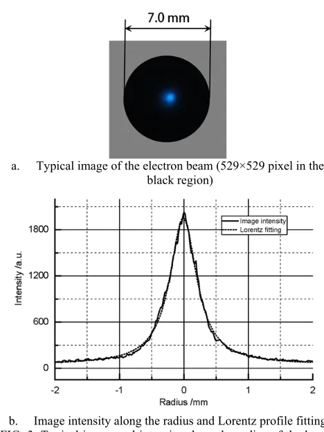
The typical image of the electron beam is shown in figure 3a. The black circular area is the phosphor screen with diameter of 7.0 mm. Because the scintillator powder is mainly stimulated by the beam electrons penetrating through the stopping copper foil, the intensity of the image should be proportional to the density of the high energy component of the beam. The relative distribution of the beam current density over its cross section can be estimated through the beam image intensity. Then the beam profile and center position of each single shot can also be obtained from the image.
According to the image intensity along a straight line across the beam center, the electron beam profile can then be determined, and the intensity can be fitted well to a Lorentz function profile shown in equation (1),
0 2 2
0
2
( )
4
A
w
I x
I
x
x
w
(1)Where I(x), I0, A, x0, x and w are the intensity of the image
at position x, the background noise intensity, constant
related to the beam intensity, beam center position, the pixel position of the beam image and FWHM of the beam profile, respectively. The FWHM of the curve shown in figure 3b is fitted as 0.53 mm.
The fitted w of the beam profiles with different hollow
[image:3.612.314.560.215.272.2] [image:3.612.60.290.231.387.2]cathode chambers and cathode apertures are presented in table I. The beam profile FWHMs (beam widths) and the standard deviations are calculated through averages of the FWHMs of corresponding single shot beam images.
TABLE I. FWHMs, in mm, of beam profiles with different pseudospark discharge configurations.
Cathode Aperture
/mm 2 3 4
SC 0.70±0.08 0.66±0.14 1.12±0.19
LC 0.63±0.17 0.52±0.09 0.46±0.16
As shown in table I, the beam widths are mainly influenced by the size of the hollow cathode cavity and are smaller with the LC configuration. The beam width can be slightly influenced by the cathode aperture size and is much smaller than the axial aperture size of the corresponding cathode, the anode and the grounded flange.
B. Beam center position distributions of different pseudospark discharge configurations
FIG. 2. Typical waveforms of the voltage and beam current. The waveforms are with LC configuration and the cathode aperture diameter is 3 mm and the nitrogen gas pressure is about 4 Pa.
a. Typical image of the electron beam (529×529 pixel in the black region)
[image:3.612.315.549.386.698.2]4
According to each of the beam images of the single shot
experiments, the beam center position (x0, y0) can be
determined through the corresponding image intensity distribution. The average of the beam positions of each
single shot (X0, Y0) can then be determined by equation (2)
and can be regarded as the intersection of the axis of the pseudospark discharge structure with the phosphor screen (abbreviated as SA in the following text),
0 0, 0 0,
1 1
1
1
X
; Y
N N
i i
i i
x
y
N
N
(2)And the distance from the beam center of each single shot to SA on the phosphor screen can be calculated through equation (3),
2
20, 0 0, 0
i i i
r
x
X
y
Y
(3)The frequencies of the electron beam centers in every 0.04 mm interval from SA in 100 shots of each
configuration are counted according to ri to study the beam
center position distributions of different pseudospark discharge configurations.
The distributions of the beam center position are shown in figure 4. It can be seen in figure 4a that the beam center
distribution of the SC configuration is more dispersed with the cathode aperture of 4 mm and the dispersion radius is about 0.68 mm from SA, while the distribution with the cathode aperture of 3 mm and 2 mm are similar but more concentrated and the dispersion radius is about 0.36 mm. The peak distributions of different configurations are not in the first 0.04 mm interval from SA and concentrates within the range of 0.04~0.12 mm for the aperture diameter of 2 mm (~60% proportion) and 3 mm (~50% proportion) and 0.08~0.16 mm for the aperture of 4 mm (~35% proportion) respectively.
The beam center distributions of the LC configuration are much more concentrated than those of the SC configuration and the dispersion radii are about 0.16 mm for the cathode apertures of 2 mm and 3 mm and about 0.24 mm for the cathode aperture of 4 mm. The distribution feature is different from that of the SC configuration, as shown in figure 4b. The beam centers concentrate within the dispersion range of 0.04 mm for the cathode aperture of 2 mm (~53% proportion) and 3 mm (~51% proportion). The beam center distribution of the LC configuration with the aperture diameter of 4 mm is more dispersed, showing a qualitative similarity to that of the SC configuration with the aperture diameter of 4 mm. The peak distribution is not in the first 0.04 mm interval from SA and concentrates within the range of 0.04~0.12 mm (~60% proportion).
C. Discussion
In this post-acceleration pseudospark-sourced electron beam configuration, the accelerated electron beam current is mainly in the conductive phase of the pseudospark discharge process. The experimental results show that the electron beam profile and the beam position distribution are quite different in the SC and LC configurations even with the same cathode aperture size, cathode-anode gap and post-acceleration gap under the same applied voltage pulse, as shown in table I and figure 4. So it can be deduced that the electron beam features can be significantly influenced by the discharge process within the hollow cathode chamber.
In the SC configuration, the beam positions are not concentrated near the axis of the structure and the peak distribution is in an annular region around the axis with different radius, which depends on the specific cathode aperture size, as shown in figure 4a. Contrasting with the SC configuration, in the LC configuration the peak distribution of the beam positions is on the axis of the structure except that the beam center distribution with the 4 mm cathode aperture shows a qualitatively similar feature with that of the SC configuration, as shown in figure 4b.
The deviation of the beam position from the axis of the SC structure may be caused by the trigger process of the pseudospark discharge. The intense electron beam originates from the electrons trapped in the low electrical field region near the axis of the hollow cathode of the pseudospark
discharge chamber18, which will be accelerated by the
a. Beam center position distribution of the SC configuration
5
electric field in the cathode-anode gap after penetrating out from the hollow cathode through the central aperture. The electron beam can be accelerated furthermore by electric fields in the post-accelerated gap. Therefore, the discharge process in the hollow cathode region can significantly influence the original position of the electron beams.
The trigger discharge gap is an annular region with 0.2 mm gap width around a 1.6 mm rod-like trigger electrode as mentioned in section II. The trigger discharge may occur in this gap at any azimuth due to the nature of randomness of the discharge process and then the deviation of the trigger discharge point from the axis may cause the deviation of the initial beam position in the hollow cathode from the axis, so that an annular distribution of the beam position on the phosphor screen can be formed by multi electron beam shots under the action of the post-acceleration voltage pulse. However, for the LC configuration with 2 mm and 3mm cathode apertures, the peak distributions of the beam center positions are on the axis of the structure. The main difference of the SC and LC configurations is the size of the hollow cathode chamber. The larger chamber will reduce the influence of the trigger discharge position and tend to initiate an electron beam on the axis of the chamber. Especially the larger depth of the hollow cathode may eliminate the influence of the deviation of the trigger discharge point from the axis when the discharge develops from the trigger point to the cathode aperture.
IV. Conclusion
In this paper, by capturing the beam image of each single shot of the high energy component of a post-accelerated pseudospark-sourced electron beam, the beam density profile on the cross section and the beam center position are obtained. The beam densities show Lorentz function profiles and the FWHM beam radii are much smaller than the aperture size, while the beam center positions disperse in a certain range around the axis of the structure depending on the specific discharge structure. The hollow cathode cavity size and cathode aperture can influence the beam profile and beam center distribution. The LC configuration can generate electron beams with smaller width and more concentrated beam center distributions. More stable electron beams can be generated especially from the LC configuration with a 3 mm cathode aperture.
ACKNOWLEDGMENTS
The authors would like to thank Mr. David Barclay of the Atoms, Beams and Plasmas group in the Department of Physics, University of Strathclyde, UK for machining the components for the experiment.
REFERENCES
1 J. Christiansen and C. Schultheiss, Zeitschrift für Physik A Atoms and
Nuclei 290, 35 (1979).
2 W. Benker, J. Christiansen, K. Frank, H. Gundel, W. Hartmann, T.
Redel, and M. Stetter, Plasma Science, IEEE Transactions on 17, 754
(1989).
3 H. Yin, W. He, A. W. Cross, A. D. R. Phelps, and K. Ronald, Journal of
Applied Physics 90, 3212 (2001).
4 L. C. Pitchford, Journal of Applied Physics 75, 7227 (1994).
5 H. Yin, G. R. M. Robb, W. He, A. D. R. Phelps, A. W. Cross, and K.
Ronald, Physics of Plasmas 7, 5195 (2000).
6 C. Q. Jiang, A. Kuthi, M. A. Gundersen, and W. Hartmann, Applied
Physics Letters 87 (2005).
7 J. Westheide, Ieee Transactions on Plasma Science 23, 254 (1995). 8 H. Yin, A. W. Cross, W. He, D. Bowes, K. Ronald, A. D. R. Phelps, J.
Protz, M. Verdiel, M. Reynolds, T. Schuhmann, X. Chen, D. Li, and J. Zhou, 2009 Ieee International Vacuum Electronics Conference, 371
(2009).
9 W. He, L. Zhang, D. Bowes, H. Yin, K. Ronald, A. D. R. Phelps, and A.
W. Cross, Applied Physics Letters 107 (2015).
10 G. Shu, W. He, L. Zhang, H. Yin, J. Zhao, A. W. Cross, and A. D. R.
Phelps, IEEE Transactions on Electron Devices PP, 1 (2016).
11 Y. Yin, W. He, L. Zhang, H. Yin, and A. W. Cross, Physics of Plasmas 22 (2015).
12 B. N. Ding, T. J. Myers, and M. J. Rhee, Review of Scientific
Instruments 64, 1442 (1993).
13 M. Nistor and N. Mandache, J. Optoelectron. Adv. Mater
7, 1619 (2005). 14 W. W. Destler, Z. Segalov, J. Rodgers, K. Ramaswamy, and M. Reiser,
Applied Physics Letters 62, 1739 (1993).
15 J. B. Zhu, Z. J. Wang, L. F. Zhang, and M. C. Wang, Ieee Transactions
on Plasma Science 24, 161 (1996).
16 E. Dewald, K. Frank, D. H. H. Hoffmann, R. Stark, M. Ganciu, B. N.
Mandache, M. G. Nistor, A. M. Pointu, and I. I. Popescu, IEEE Transactions on Plasma Science 25, 272 (1997).
17 J. Zhao, H. Yin, L. Zhang, G. Shu, W. He, J. Zhang, Q. Zhang, A. D. R.
Phelps, and A. W. Cross, Physics of Plasmas 23, 073116 (2016). 18 L. Pitchford, J. P. Boeuf, V. Puech, R. Liou, and M. Gundersen,