Semiconductor Devices:
Semiconductor Devices:
Theory and Application
Theory and Application
James M. Fiore
Semiconductor Devices:
Semiconductor Devices:
Theory and Application
Theory and Application
by
James M. Fiore
This Semiconductor Devices: Theory and Application, by James M. Fiore is copyrighted under the terms of a Creative Commons license:
This work is freely redistributable for non-commercial use, share-alike with attribution
Device data sheets and other product information are copyright by their respective owners
Published by James M. Fiore via dissidents
For more information or feedback, contact: James Fiore, Professor
Electrical Engineering Technology Mohawk Valley Community College 1101 Sherman Drive
Utica, NY 13501
For the latest revisions, related titles and links to low cost print versions, go to
www.mvcc.edu/jfiore or www.dissidents.com
Preface
Preface
Welcome to the first edition of Semiconductor Devices, an open educational resource (OER). The goal of this text, as its name implies, is to allow the reader to become proficient in the analysis and design of circuits utilizing discrete semiconductor devices. It progresses from basic diodes through bipolar and field effect transistors. The text is intended for use in a first or second year course on semiconductors at the Associate or Baccalaureate level. In order to make effective use of this text, students should have already taken coursework in basic DC and AC circuits, and have a solid background in algebra and trigonometry along with exposure to phasors. Calculus is used in certain sections of the text but for the most part it is used for equation derivations and proofs, and is kept to a minimum. For students without a calculus background these sections may be skipped without a loss of continuity.
An OER companion laboratory manual is also available. It features nearly 30 exercises that parallel the topics presented in this text. For continued study, a follow-on OER text and lab manual, Operational Amplifiers and Linear Integrated Circuits, Third Edition is available. Several other electrical OER titles are also available. I cannot say enough about the emerging Open Educational Resource movement and I encourage budding authors to consider this route. While there are (generally) no royalties to be found, having complete control over your own work (versus the “work for hire” classification of typical contracts) is not to be undervalued. Neither should contributions to the profession nor the opportunity to work with colleagues be dismissed. Given the practical aspects of the society in which we live, I am not suggesting that people “work for free”. Rather, because part of the mission of institutes of higher learning is to promote and disseminate formalized instruction and information, it is incumbent on those institutions to support their faculty in said quest, whether that be in the form of sabbaticals, release time, stipends or the like. It is also my opinion that no one should be deprived of a higher education due to lack of funds. A society that truly cares for its citizens would institute free college tuition.
If you have any questions regarding the text or lab manual, or are interested in contributing to the project, do not hesitate to contact me. Finally, please be aware that the most recent versions of all of my OER texts and manuals may be found at my MVCC web site as well as my mirror site: www.dissidents.com
Acknowledgements
Acknowledgements
For their continued support, my family and friends. For their input on draft versions, my colleagues (esp. Ben Glallard, Hill Bunt, Deb Bocker, Hal Paulko, Thom Timas) and students. For on-going sanity reassurance, Bernie Sanders and Mike Lofgren. For unintentional diversionary humor elicitation, Wally and pals. Finally, a serious thank you, thank you, thank you to all of the people who have created useful software and other OER tools without which this project would have been impossible. When we each do a little, we all gain a lot. This text was created using several free and open software applications including Open Office and Dia. Some graphs and device curves were created using SciDAVis. Screen imagery was often manipulated though the use of XnView.
For Karen
Table of Contents
Table of Contents
Chapter 1: Semiconductor Fundamentals
Chapter 1: Semiconductor Fundamentals
14
14
1.0 Chapter Objectives .
.
.
.
.
.
.
14
1.1 Introduction
.
.
.
.
.
.
.
14
First, a Little History
Variable Naming Convention
1.2 Atomic Structure .
.
.
.
.
.
.
16
1.3 Crystals
.
.
.
.
.
.
.
.
20
1.4 Doped Materials
.
.
.
.
.
.
.
23
N-Type Material P-Type Material
Summary
.
.
.
.
.
.
.
.
27
Review Questions
.
.
.
.
.
.
.
27
Chapter 2: PN Junctions and Diodes
Chapter 2: PN Junctions and Diodes
29
29
2.0 Chapter Objectives .
.
.
.
.
.
.
29
2.1 Introduction
.
.
.
.
.
.
.
29
2.2 The PN Junction
.
.
.
.
.
.
.
30
Forward-Bias Reverse-Bias Shockley Equation
2.3 Diode Data Sheet Interpretation
.
.
.
.
.
35
2.4 Diode Circuit Models
.
.
.
.
.
.
39
2.5 Other Types of Diodes
.
.
.
.
.
.
47
Zener Diode
Light Emitting Diode and Photodiode Schottky and Varactor Diodes
Summary
.
.
.
.
.
.
.
.
55
Review Questions
.
.
.
.
.
.
.
55
Problem Set
.
.
.
.
.
.
.
.
55
Chapter 3: Diode Applications
Chapter 3: Diode Applications
63
63
3.0 Chapter Objectives .
.
.
.
.
.
.
63
3.1 Introduction
.
.
.
.
.
.
.
63
3.2 Rectification
.
.
.
.
.
.
.
63
Half-wave Rectification A Note Regarding Transformers Smoothing (Filtering) the Output Full-wave Rectification
3.3 Clippers
.
.
.
.
.
.
.
.
80
3.4 Clampers .
.
.
.
.
.
.
.
83
Summary
.
.
.
.
.
.
.
.
86
Review Questions
.
.
.
.
.
.
.
86
Problem Set
.
.
.
.
.
.
.
.
87
Chapter 4: Bipolar Junction Transistors (BJTs)
Chapter 4: Bipolar Junction Transistors (BJTs)
90
90
4.0 Chapter Objectives .
.
.
.
.
.
.
90
4.1 Introduction
.
.
.
.
.
.
.
90
4.2 The Bipolar Junction Transistor
.
.
.
.
.
90
A Simple Two-Diode Model Biasing the BJT The PNP Bipolar Junction Transistor
4.3 BJT Collector Curves.
.
.
.
.
.
.
95
Rise in β and Early Voltage
4.4 BJT Data Sheet Interpretation
.
.
.
.
.
98
4.5 Ebers-Moll Model .
.
.
.
.
.
.
101
β Variation Issues
4.6 DC Load Lines
.
.
.
.
.
.
.
104
4.7 BJT Switching and Driver Applications
.
.
.
.
106
The Saturating Switch The Non-Saturating Driver The Zener Follower
Summary
.
.
.
.
.
.
.
.
111
Review Questions
.
.
.
.
.
.
.
112
Problem Set
.
.
.
.
.
.
.
.
112
Chapter 5: BJT Biasing
Chapter 5: BJT Biasing
116
116
5.0 Chapter Objectives .
.
.
.
.
.
.
116
5.1 Introduction
.
.
.
.
.
.
.
116
5.2 The Need For Biasing
.
.
.
.
.
.
116
5.3 Two-Supply Emitter Bias
.
.
.
.
.
.
117
Verification of Stability PNP Two-Supply Emitter Bias
5.4 Voltage Divider Bias.
.
.
.
.
.
.
123
Verification of Stability PNP Voltage Divider Bias
5.5 Feedback Biasing .
.
.
.
.
.
.
130
Summary
.
.
.
.
.
.
.
.
135
Review Questions
.
.
.
.
.
.
.
135
Problem Set
.
.
.
.
.
.
.
.
136
Chapter 6: Amplifier Concepts
Chapter 6: Amplifier Concepts
141
141
6.0 Chapter Objectives .
.
.
.
.
.
.
141
6.1 Introduction
.
.
.
.
.
.
.
141
6.2 Amplifier Model
.
.
.
.
.
.
.
141
Loading Effects
6.3 Compliance and Distortion .
.
.
.
.
.
144
6.4 Frequency Response and Noise
.
.
.
.
.
149
6.5 Miller's Theorem. .
.
.
.
.
.
.
151
Summary
.
.
.
.
.
.
.
.
154
Review Questions
.
.
.
.
.
.
.
155
Problem Set
.
.
.
.
.
.
.
.
155
Chapter 7: BJT Small Signal Amplifiers
Chapter 7: BJT Small Signal Amplifiers
158
158
7.0 Chapter Objectives .
.
.
.
.
.
.
158
7.1 Introduction
.
.
.
.
.
.
.
158
7.2 Simplified AC Model of the BJT
.
.
.
.
.
159
7.3 Common Emitter Amplifier .
.
.
.
.
.
162
Voltage Gain Input Impedance Output Impedance Power Supply Bypass and Decoupling
7.4 Common Collector Amplifier
.
.
.
.
.
175
Voltage Gain Input Impedance Output Impedance A High Impedance Source: The Guitar Pickup The Darlington Pair The Phase Splitter
7.5 Common Base Amplifier
.
.
.
.
.
.
186
Voltage Gain Input Impedance Output Impedance
7.6 Multi-Stage Amplifiers
.
.
.
.
.
.
188
Direct Coupling
Summary
.
.
.
.
.
.
.
.
191
Review Questions
.
.
.
.
.
.
.
191
Chapter 8: BJT Class A Power Amplifiers
Chapter 8: BJT Class A Power Amplifiers
199
199
8.0 Chapter Objectives .
.
.
.
.
.
.
199
8.1 Introduction
.
.
.
.
.
.
.
199
8.2 Amplifier Classes .
.
.
.
.
.
.
199
8.3 Class A Operation and Load Lines .
.
.
.
.
200
8.4 Loudspeakers
.
.
.
.
.
.
.
211
Loudspeaker Impedance
8.5 Power Transistor Data Sheet Interpretation .
.
.
.
216
Power Derating
8.6 Heat Sinks .
.
.
.
.
.
.
.
220
Thermal Resistance
Summary
.
.
.
.
.
.
.
.
226
Review Questions
.
.
.
.
.
.
.
226
Problem Set
.
.
.
.
.
.
.
.
226
Chapter 9: BJT Class B Power Amplifiers
Chapter 9: BJT Class B Power Amplifiers
231
231
9.0 Chapter Objectives .
.
.
.
.
.
.
231
9.1 Introduction
.
.
.
.
.
.
.
231
9.2 The Class B Configuration .
.
.
.
.
.
232
Class AB Operation The Current Mirror Class B Circuit Maximums Class B Power Dissipation Class B Efficiency
9.3 Extensions and Refinements
.
.
.
.
.
251
Current Limiting High Current Gain Configurations Current Sharing VBE Multiplier and Miller Capacitor Bridging Power Supply Bypassing
Summary
.
.
.
.
.
.
.
.
259
Review Questions
.
.
.
.
.
.
.
260
Problem Set
.
.
.
.
.
.
.
.
260
Chapter 10: Junction Field Effect Transistors (JFETs)
Chapter 10: Junction Field Effect Transistors (JFETs)
266
266
10.0 Chapter Objectives
.
.
.
.
.
.
266
10.1 Introduction
.
.
.
.
.
.
.
266
10.2 JFET Internals
.
.
.
.
.
.
.
267
10.3 JFET Data Sheet Interpretation
.
.
.
.
.
272
10.4 JFET Biasing
.
.
.
.
.
.
.
275
DC ModelConstant Voltage Bias Self Bias
Constant Current Bias
Summary
.
.
.
.
.
.
.
.
291
Review Questions
.
.
.
.
.
.
.
292
Problem Set
.
.
.
.
.
.
.
.
292
Chapter 11: JFET Small Signal Amplfiers
Chapter 11: JFET Small Signal Amplfiers
296
296
11.0 Chapter Objectives
.
.
.
.
.
.
296
11.1 Introduction
.
.
.
.
.
.
.
296
11.2 Simplified AC Model of the JFET .
.
.
.
.
296
11.3 Common Source Amplifier.
.
.
.
.
.
297
Voltage Gain Input Impedance Output Impedance
11.4 Common Drain Amplifier .
.
.
.
.
.
306
Voltage Gain Input Impedance Output Impedance
11.5 Multi-stage and Combination Circuits
.
.
.
.
309
11.6 Ohmic Region Operation .
.
.
.
.
.
311
Summary
.
.
.
.
.
.
.
.
316
Review Questions
.
.
.
.
.
.
.
317
Problem Set
.
.
.
.
.
.
.
.
317
Chapter 12: Metal Oxide Semiconductor FETs (MOSFETs)
Chapter 12: Metal Oxide Semiconductor FETs (MOSFETs)
321
321
12.0 Chapter Objectives
.
.
.
.
.
.
321
12.1 Introduction
.
.
.
.
.
.
.
321
12.2 The DE-MOSFET .
.
.
.
.
.
.
322
12.3 DE-MOSFET Biasing
.
.
.
.
.
.
325
Zero Bias Voltage Divider Bias
12.4 The E-MOSFET
.
.
.
.
.
.
.
328
12.5 E-MOSFET Data Sheet Interpretation
.
.
.
.
331
12.6 E-MOSFET Biasing .
.
.
.
.
.
.
334
Voltage Divider Bias Drain Feedback Bias
Summary
.
.
.
.
.
.
.
.
337
Review Questions
.
.
.
.
.
.
.
338
Chapter 13: MOSFET Small Signal Amplifiers
Chapter 13: MOSFET Small Signal Amplifiers
344
344
13.0 Chapter Objectives
.
.
.
.
.
.
344
13.1 Introduction
.
.
.
.
.
.
.
344
13.2 MOSFET Common Source Amplifiers
.
.
.
.
344
Voltage Gain Input Impedance Output Impedance
13.3 MOSFET Common Drain Followers
.
.
.
.
352
Voltage Gain Input Impedance Output Impedance
Summary
.
.
.
.
.
.
.
.
356
Review Questions
.
.
.
.
.
.
.
357
Problem Set
.
.
.
.
.
.
.
.
357
Chapter 14: Class D Power Amplifiers
Chapter 14: Class D Power Amplifiers
362
362
14.0 Chapter Objectives
.
.
.
.
.
.
362
14.1 Introduction
.
.
.
.
.
.
.
362
14.2 Class D Basics
.
.
.
.
.
.
.
363
14.3 Pulse Width Modulation .
.
.
.
.
.
365
Reconstituting the Output
14.4 Output Configurations
.
.
.
.
.
.
368
Practical Concerns
Summary
.
.
.
.
.
.
.
.
376
Review Questions
.
.
.
.
.
.
.
377
Problem Set
.
.
.
.
.
.
.
.
377
Chapter 15: Insulated Gate Bipolar Transistors (IGBTs)
Chapter 15: Insulated Gate Bipolar Transistors (IGBTs)
378
378
15.0 Chapter Objectives
.
.
.
.
.
.
378
15.1 Introduction
.
.
.
.
.
.
.
378
15.2 IGBT Internals
.
.
.
.
.
.
.
379
15.3 IGBT Data Sheet Interpretation
.
.
.
.
.
381
15.4 IGBT Applications .
.
.
.
.
.
.
389
Induction Heating DC-to-AC Inversion Motor Control DC-to-DC Conversion
Summary
.
.
.
.
.
.
.
.
395
Review Questions
.
.
.
.
.
.
.
396
Appendices
Appendices
398
398
A: Manufacturer's Data Sheet Links
.
.
.
.
.
398
B: Standard Component Sizes .
.
.
.
.
.
399
1
1
Semiconductor Fundamentals
Semiconductor Fundamentals
1.0 Chapter Learning Objectives
1.0 Chapter Learning Objectives
After completing this chapter, you should be able to:
• Define the term semiconductor.
• Describe the differences between conductors, semiconductors and insulators in terms of atomic energy levels.
• Describe the atomic structure of mono-crystalline silicon.
• Detail the effect of doping on a silicon crystal.
• Describe the differences between P material and N material.
• Draw the energy level diagrams for P- and N-type materials.
1.1 Introduction
1.1 Introduction
First, a Little History
First, a Little History
Just as the late eighteenth through nineteenth centuries are known as the industrial age due to the rise of mechanization, the twentieth century can be referred to as the beginning of the electronic age. The first half of the century was dominated by electronic vacuum tubes that made possible devices such as radio, television, radar and long distance telephone. The technology of the vacuum tube was displaced mid-century by the introduction of solid-state semiconductors. The first working prototype transistor was invented at Bell Labs in 1947 by John Bardeen, Walter Brattain and William Shockley. This device, properly referred to as a point contact transistor, was quickly superseded by the bipolar junction transistor, a major topic of this text.
Commercial production of the transistor and related devices improved the performance of existing applications and made possible a range of new ones. Semiconductors proved to be smaller, lighter, more reliable and less expensive to build than their vacuum tube counterparts. The last 30 or so years of the century saw the rapid expansion of the integrated circuit where numerous transistors are combined in a single device. Initially such a device may have contained the equivalent of a dozen or so individual semiconductor devices, but today that number has grown to the billions1. This extreme density has given rise to now common-place applications such
as cell phones, GPS devices, laptop computers, tablets and our global communications infrastructure.
The science writer, Arthur C. Clarke, once observed that “Any sufficiently advanced technology is indistinguishable from magic”. Indeed, although today the typical citizen living in an industrialized country makes use of numerous electronic devices each day (sometimes without even being aware of it), they typically have scant knowledge of how these devices “work their magic”. Obviously there is no magic, only the application of scientific principles mixed with human ingenuity. Further, just as it is true that many more people can use a cell phone than design one, it is also true that there is a greater need for people who can design, manufacture and maintain devices based on semiconductors than for people who design the semiconductors themselves. The scope of this text, then, focuses on the operation and application of semiconductor devices rather than the design of the
semiconductors themselves.
Variable Naming Convention
Variable Naming Convention
One item that often confuses beginning students of almost any subject is nomenclature. Before we begin our discussion of semiconductor devices it is important that we decide upon a consistent naming convention. Throughout this text we will be examining numerous circuits containing several passive and active components. We will be interested in a variety of parameters and signals. In order to keep confusion to a minimum we will use the following conventions in our
equations for naming devices and signals.
R Resistor (DC, or actual circuit component)
r Resistor (AC equivalent, where phase is 0 or ignored)
C Capacitor
L Inductor
Q Transistor (Bipolar or FET)
D Diode
V Voltage (DC)
v Voltage (AC)
I Current (DC)
i Current (AC)
Resistors, capacitors and inductors are differentiated via a subscript that usually refers to the active device to which it is connected. For example, RE is a DC bias
resistor connected to the emitter of a transistor while rC refers to the AC equivalent
resistance seen at a transistor’s collector. CE refers to a capacitor connected to a
transistor’s emitter lead. Note that the device related subscripts are always shown in upper case, with one exception: If the resistance or capacitance is part of the device model, the subscript will be shown in lower case to distinguish it from the external circuit components. For example, the AC dynamic resistance of a diode would be called rd. If no active devices are present or if several items exist in the circuit, a
simple numbering scheme is used, such as R1. In very complex circuits a specific
Voltages are normally given a two-letter subscript indicating the nodes at which it is measured. VXY is the DC potential from node X to node Y while vXY indicates the AC
signal appearing across node X to node Y. A single-letter subscript, as in VX,
indicates a potential relative to ground (in this case from node X to ground). The exceptions to this rule are power supplies, that are given a double letter subscript indicating the connection point (VCC is the collector power supply), and particularly
important potentials that are directly named, as in vin (AC input voltage) and VR2 (DC
voltage appearing across R2). If an equation for a specific potential is valid for both
the AC and DC equivalent circuits, the uppercase form is preferred (this makes things more consistent with circuits that are directly coupled, and thus can amplify both AC and DC signals). Currents are named in a similar way but generally use a single subscript referring to the measurement node (IX is the DC current flowing
through a conductor into or out of node X). All other items are directly named. By using this scheme, you will always be able to determine whether the item expressed in an equation is a DC or AC equivalent, its approximate circuit location, and other factors about it.
1.2 Atomic Structure
1.2 Atomic Structure
In our effort to understand the operation of semiconductors, a fundamental question we might ask is “What is the internal structure of an atom?” Please understand that it is nonsensical to ask what an atom might “look like” because its components are all smaller than the shortest wavelengths of light that humans can see. Instead, we simply need a model to explain its observed behavior.
Perhaps the most prolific model in the popular imagination is the planetary model
shown in Figure 1.1. In this model, the core, or nucleus, is drawn at the center and contains positively charged protons and non-charged neutrons. Revolving around this core are negatively charged electrons, each following a nice, regular, planar path much like a planet around the sun. Unfortunately for us, this model is starkly incorrect, although it has found use as a symbol for nuclear regulatoryagencies
and a DEVOalbum cover from the 1970s.
Before we come up with a more accurate and useful model, let's take a closer look at the sub-components; namely the proton, neutron and electron. First off, most of the mass of any given atom is from the protons and neutrons. Protons and neutrons have similar masses, about 1.67E-24 grams each. The mass of an electron is roughly 2000 times smaller. The radius of a proton is approximately 0.87E-15 meters and the mean distance to the nearest electron is about 5.3E-11 meters. This means that this electron is about 60,000 times farther away from the proton than the size of said proton. To put this into perspective, that's roughly the same as the ratio between a golf ball and a sphere with a radius of 3/4ths of a mile or 1200 meters. This would be the case for a hydrogen atom as it consists of a single proton and electron. The magnitude of this ratio is not much different for other substances, including things
Figure 1.1
like crystalline carbon (diamond) and quartz (a molecule of silicon and oxygen) that are very hard and solid. If you think about that for a moment, you realize that the idea of “solidity” is in some ways an illusion because the vast majority of what we call “something” is really just empty space. For example, chances are that you are sitting down while reading this. You probably feel your buttocks pressed against the chair. Both of these things are considered solid yet at the atomic level the vast majority of both items is nothingness. In reality, the feeling of solidity is just the result of the interaction of atomic forces between the two. So if someone suggests that you might have a bit too much to spare in the department of the posterior, you can inform them that it's really nothing.
One of the major issues with the planetary model is the idea that electrons whirl around the nucleus in stable, planet-like orbits. That's simply not true. First, the electron inhabits a region of 3D space, it does not simply move through a plane. Second, due to the Heisenberg Uncertainty Principle, we can't precisely plot the position and trajectory of a given electron. The best we can do is make a plot of where the electron is likely to be. This is called a probability contour. Imagine that you could record the position of an electron relative to the nucleus. A moment later you record its new position, a moment after that you record the next position, and on and on for thousands of measurements. If you attempted to plot them all, you would wind up with a cloud of dots around the nucleus. This cloud is referred to as an
orbital. You wouldn't know how the electron got from one position to the next but you would get a general idea of where it was likely to be. Do not confuse orbital
with orbit (like a planetary orbit). They are two different beasties.
There are several potential orbitals. Due to quantum physics, only certain orbitals are allowed. The permissible electron energy levels are first grouped into shells, then
subshells and finally orbitals.It is important to remember that orbitals indicate the electron energy level. That is, a higher orbital implies a higher energy level. Further, orbitals fill in first from lowest energy level to highest energy level. These are important ideas that we will leverage in future discussions.
Shells are denoted by their principal quantum number, n; 1, 2, 3, etc. The higher the number, the more subshells it can contain. Subshells are organized by their orbital shape and are designated by letters, the first four being s, p, d, and f. Shell 1
contains only subshell s while shell 2 contains subshell types s and p. Shell 3
contains subshell types s, p and d, and so on.
Thus, we see designations such as 1s, 2s and 2p. These subshells may also have variations within them. There is one variation on s, three variations on p, five variations on d, etc. These variations are the orbitals and each orbital can hold a maximum of two electrons.
Putting this all together, we find that the first shell can contain a maximum of two electrons: two in the single s subshell orbital (1s). The second shell can contain a maximum of eight electrons: two in the s subshell (2s) plus two in each of the three
Figure 1.2
p subshell orbitals (2p). In like manner the third shell can contain a maximum of 18 electrons: two in 3s, six in 3p and two in each of the the five d subshell orbitals (3d). You can condense this into a simple formula, 2n2, where n is the shell number.
Figure 1.2 shows the electron probability contour of the innermost orbital, namely
1s (i.e., principle quantum number 1, subshell s). As you can see, it is spherical in shape. The nucleus is located at the center, obscured here. All s orbitals are similarly spherically shaped although the internals change. 1s is the lowest energy orbital. Orbitals are not limited to simple spherical shapes. Higher order orbitals can take on a variety of forms. Figure 1.3 shows the electron probability contour for the 2p
orbitals (recall there are three p variations, one each oriented along the X, Y and Z axes). The nucleus is situated in the small void between the two lobes. Obviously, this is nothing like the well-behaved elliptical orbits of planets around the sun. Probability contours can be very complex. For the highest orbitals, especially when combined with the lower orbitals, the contour combinations can become reminiscent of the sculptures of a deranged clown forming herds of imaginary balloon animals.
As interesting as these graphics are, they are cumbersome to work with.
Consequently, a more functional graphic is called for. Such a device is the Bohr model, named after Danish physicist Niels Bohr. An example is shown in Figure 1.4. It is important to understand that the Bohr model is an energy description of the atom, not an attempt to mimic its physical appearance or structure. The nucleus is placed at the center. It is surrounded by concentric rings that represent the electron shells. The higher the number, the larger the ring and the greater the energy level. If an electron were to move from a higher level to a lower level, the energy difference is radiated out. This could be in the form of heat or light. This is a point worth remembering. For example, this transition is what makes light emitting diodes (LEDs) function. The inverse is also possible, namely that by absorbing energy, an electron can move into a higher orbital. This is an equally powerful concept, as we shall soon see.
Using the Bohr model we can create diagrams to represent individual elements. For example, copper has an atomic number of 29 meaning that it has 29 protons and 29 electrons. The electron shell configuration is 2-8-18-1. That is, the first three shells are completely filled and there is a single electron in the fourth shell. This single outer electron is only loosely bound and thus makes copper a very good conductor. The Bohr model for copper would simply show four rings, the first three being filled and with a single electron in the fourth ring.
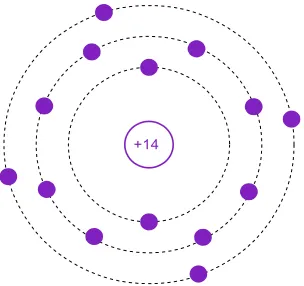
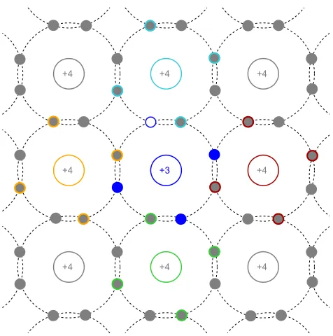
Figure 1.5 shows the Bohr model of an atom of Silicon, atomic number 14, with an electron shell configuration of 2-8-4. In this version, the individual electrons are drawn in each shell and the atomic number is indicated at the nucleus. Again, please do not imagine this representing individual electrons orbiting the nucleus in lanes. This is an energy level depiction.
Figure 1.3
Electron probability contour for orbital 2p.
Image source
Figure 1.4
Often, it is useful to simplify this model further by omitting the filled inner shells. Also, the atomic number is replaced by the number of electrons in the outermost, or
valence, shell. This is shown in Figure 1.6. The valence shell is particularly important as it gives insight into the general behavior of the material.
As an alternative, sometimes we will “straighten out” the Bohr model so that it simply shows the energy levels graphically as lines or bands, and without counting specific electrons. This is depicted in Figure 1.7.
[image:19.612.170.322.72.215.2]+14
Figure 1.5
Bohr model of Silicon.
+4
Figure 1.6
Simplified Bohr model of Silicon.
Energy
[image:19.612.160.330.500.669.2]n=1 n=2 n=3 n=4
Figure 1.7
1.3 Crystals
1.3 Crystals
We used silicon in the preceding example on purpose. The fact that it has a half-filled valence shell with four electrons puts it in a special place. As is, it's neither a great conductor nor a superior insulator. With some attention to detail, it will become a semiconductor. Silicon is not the only material that can be used for semiconductors. In fact, many of the earliest semiconductors were made from germanium and currently we make semiconductors from other materials. Silicon, however, remains the source of most semiconductors today.
It is possible for pure silicon to be arranged in a mono crystaline structure. That is, all of the silicon atoms align in a very specific, well-ordered manner, without any voids or breaks in the pattern. As silicon has only four electrons in its valence shell, four more electrons would be needed to fill the shell. In the crystal, any given atom of silicon effectively “shares” an electron from its four closest neighbors through a
covalent bond (meaning “with or among the valence”). Each atom does this,
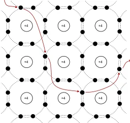
therefore each atom is tightly bound to its neighbors. This is illustrated in Figure 1.8 using simplified Bohr models. Note the color coding that indicates the sharing.
Remember, this is an energy diagram. We are not trying to indicate that individual valence electrons are zipping between atoms in figure eight patterns. Indeed, this diagram is drawn flat whereas a real crystal is not a simple sheet, but is three dimensional with varying thickness.
+4 +4 +4
+4 +4 +4
[image:20.612.120.385.336.595.2]+4 +4 +4
Figure 1.8
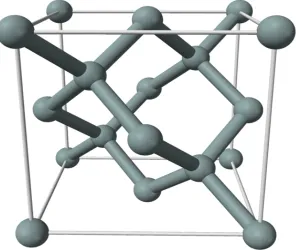
While it would be a practical impossibility to draw a highly realistic representation of atoms in the crystal, given a few liberties we can draw something that at least comes a little closer to reality. We start by representing each silicon atom as a ball and the covalent bond as a connecting tube. Recalling that each atom must be bound to four others in a regular, equal pattern, we come up with the drawing of Figure 1.9. Notice that the overall structure is essentially that of a cube. Further, at the center of each face of the cube there exists an atom of silicon. Therefore, we say that the crystal structure is face centered cubic.
[image:21.612.99.395.198.448.2]An interesting thing happens in the crystal when we examine the energy levels. With a single atom we would expect to see an energy diagram like that of Figure 1.7. That is, discrete, permissible steps. Within a crystal, though, each atom is affected by those around it. This causes slight changes in the energy levels. Taken as a whole, all of these individual variations cause the discrete levels to blur into broader bands. If we were to examine the valence and conduction energy levels, instead of discrete, thin lines we'd see the thicker bands as illustrated in Figure 1.10. These bands still represent permissible electron energy levels, it's just that now there is a continuum rather than a discrete level. There will still be non-permissible or forbidden zones between these regions. A forbidden zone is referred to as a band gap.
Figure 1.9
Representation of silicon crystal structure.
Associated with this idea is the concept of the Fermi level, named after physicist
Enrico Fermi. Basically, the Fermi level is the energy level in a given material at which there is a 50% probability that it is filled with electrons. In other words, levels below this value tend to be filled with electrons and levels above tend to be empty. If the Fermi level lies within a band, the material will be good a conductor. On the other hand, if the Fermi level lies between two widely separated bands,
the material will be a good insulator. If the Fermi level is between bands that are relatively close, the material is a semiconductor.
Figure 1.10 shows the energy bands for an intrinsic semiconductor, such as an ideal silicon crystal. The term intrinsic simply means that there are no impurities in the crystal. Between the valence band and conduction band is an impermissible or forbidden region. This is a band gap. In practical terms you can think of the band gap as the amount of energy that needs to be applied to an electron in order to move it from the valence band to the conduction band. The value of the band gap will depend on a variety of factors, the precise material being used for the semiconductor is of particular importance.
[image:22.612.379.570.90.308.2]Without any external energy applied (i.e., isolated and at absolute zero), the crystal lattice is stable and there is no electron movement through the crystal. As we add thermal energy, it is possible for valence electrons to jump up to the conduction band. At this point, the electron can “wander” through the crystal in the manner depicted in Figure 1.11.
Figure 1.10
Energy diagram for an intrinsic semiconductor.
Energy
valence band conduction band
Fermi level forbidden region
+4 +4 +4
+4 +4 +4
[image:22.612.108.373.420.670.2]+4 +4 +4
Figure 1.11
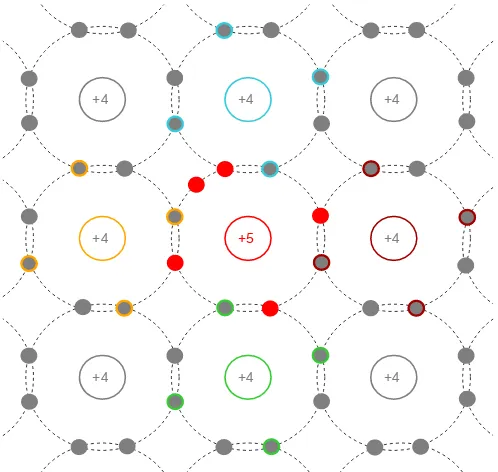
Here is how this happens: Because the thermal energy causes the electron to jump to the higher energy level of the conduction band, it leaves behind a “hole”, that is, a place devoid of an electron. Now that the hole exists, it provides a place for another electron to “fall into”. The higher the temperature, the greater the number of freed electrons and the greater the number of corresponding holes. We now have thermally-induced electron movement. We can also look at this from the opposing perspective, namely that we have an equal magnitude but opposite direction “hole flow”. If you find this idea hard to grasp, simply look at Figure 1.12. Each horizontal bar contains four dots representing electrons. In the topmost bar there is an empty space (a hole) to the extreme left. When the leftmost electron moves into this hole it fills it in a process called electron-hole recombination, which of course, sounds much more impressive than it really is. The result is the second bar. We repeat this process of moving an electron right to left as we traverse down the diagram. Eventually we end up with the four electrons packed together toward the left. Finally, instead of focusing on the dots, focus instead on the negative space (the empty white bit). Moving from top to bottom, the hole moves left to right, in the opposing direction.
Just as we think of the movement of electrons as a movement of negative charge, then the movement of holes can be thought of as a movement of positive charge. We can say that the electron is the carrier of negative charge while the hole is the carrier of positive charge.
Before moving on to the next section, it is important to remember that in an intrinsic (pure) semiconductor, the number of thermally produced electrons and holes will be equal. Also, even at room temperature the total number will also be quite small compared to the number of electrons in the crystal.
1.4 Doped Materials
1.4 Doped Materials
By themselves, intrinsic semiconductors are not of particular use. They are neither good conductors nor insulators, and their conduction is largely dependent on temperature. We can alter the properties of the material by introducing foreign substances or impurities into the crystal. These impurities are also known as
dopants. A crystal with an added dopant is referred to as an extrinsic semiconductor or doped material. The amount of impurity added is generally small, perhaps in the neighborhood of one part per million. The dopant may be added through a gaseous diffusion process where the crystal is heated in an oven and the dopant added in gaseous form. Over a period of time the impurities will diffuse or “seep into” the target crystal. An alternate approach is ion implantation. In this method the impurities are accelerated and quite literally smash into the target, dislodging and replacing some of the original atoms in the crystal.
Figure 1.12
There are two different types of semiconductors possible. One is called N-type material, and the other, P-type material. Unsurprisingly, the N stands for Negative and the P stands for (you guessed it) Positive. N-type material is created by adding pentavalent impurities, that is, a dopant with five electrons in its outer shell. Examples include phosphorus, arsenic and antimony. In contrast, P-type material is created by adding a trivalent impurity, one with three electrons in its outer shell. Possible trivalent impurities include boron, gallium and indium.
N-Type Material
N-Type Material
Figure 1.13 shows a model of a silicon crystal with a pentavalent impurity at its center. Compared to an ordinary silicon atom that would have four electrons in its outer shell, the pentavalent impurity creates an extra, or donor, electron. Thus, the crystal has a net negative charge and is referred to as N-type material. The energy level of the donor electrons is just below the bottom of the conduction band. In other words, the difference between the donor level and the bottom of the conduction band is much, much smaller than the band gap itself. Therefore it is relatively easy for these donor electrons to jump into the conduction band, becoming free ionized electrons and leaving behind ionized holes2.
[image:24.612.121.370.356.592.2]2 An ion is an atom or molecule that does not have a neutral net charge, i.e., the numbers of protons and electrons are not equal. If it loses electrons, resulting in a net positive charge, it is called a cation. If it gains electrons resulting in a net negative charge it is called an anion.
Figure 1.13
Crystal with added pentavalent impurity (N-type).
+4 +4 +4
+4 +5 +4
Compared to the undoped intrinsic crystal, the doped extrinsic crystal exhibits a relatively high number of free electrons. As you might surmise, this enhances the conductivity of the material, and the greater the doping level, the greater the enhancement. Earlier it was mentioned that both electrons and holes can serve as charge carriers. Because the number of free electrons is significantly larger than the number of holes in N-type material, electrons in N-type material are referred to as the majority charge carrier (or more simply, the majority carrier) while holes are referred to as the minority charge carrier (or minority carrier).
The extra electrons add to the number of filled energy states and, being of higher energy than the valence electrons, push the Fermi level to a higher value.
Remember, the Fermi level represents the point where 50% of states would be filled, so if we add states above this, then the new 50% point must be higher than the former level. This is illustrated in Figure 1.14. Note how close the donor level is to the conduction band and that the Fermi level has been pushed up, away from the valence band and closer to the conduction band. This will be of great significance in up-coming discussions on semiconductor devices.
P-Type Material
P-Type Material
In a similar manner, if we introduce a trivalent impurity, our crystal model now features a hole; a location where an electron is lacking. For this reason, trivalent impurities are sometimes called acceptors. The resulting crystal model is illustrated in Figure 1.15.
Energy
valence band conduction band
new higher Fermi level donor level
- ionized electrons
N material
- - -
-Figure 1.14
The resulting situation is essentially the reverse of that of the N-type material. Figure 1.16 shows the energy band diagram for our new P-type material. In this case, the Fermi level has been pushed down, closer to the valence band.
In P-type material, holes out number free electrons. Consequently, holes are referred to as the majority carrier in P material while electrons take on the role of minority charge carrier.
Figure 1.15
Crystal with added trivalent impurity (P-type).
+4 +4 +4
+4 +3 +4
[image:26.612.116.354.76.316.2]+4 +4 +4
Figure 1.16
Energy band diagram of P-type semiconductor.
Energy
valence band conduction band
new lower Fermi level
acceptor level
+
ionized holes P material
As with N-type material, the greater the amount of trivalent impurity added, the greater the overall effect. By itself, a doped crystal can be used to create a resistor. The resistivity of the material is a function of the doping level. By setting the cross- sectional area, length and doping level, we can create well-defined resistor values. If this was all we could do with semiconductors then we could say two things: first, the solid state semiconductor revolution would not exist; and second, this text would be very short. The interesting bits arrive when we combine both N- and P-type
materials into a single device, as we shall begin to see in the next chapter.
Summary
Summary
In this chapter we have examined the basic structure of atoms. This includes the concept of electron shells and permissible energy states. We have used both the Bohr model of the atom and the corresponding energy band diagrams.
Crystals such as silicon show a very ordered three dimensional structure that relies on strong covalent bonds. The crystal tends to “fuzz” or broaden the permissible energy levels into thicker energy bands. Further, the crystal exhibits a modest energy gap, or band gap, between the valence band and conduction band. This gap is much smaller than the gap seen in insulators, and therefore the material is referred to as a semiconductor, being somewhere between a true conductor and a true insulator.
The electrical characteristics of a pure, or intrinsic, semiconductor crystal can be altered by adding impurities or dopants. A doped crystal is referred to as an extrinsic crystal. If a pentavalent dopant is added, there will be a surplus of electrons and a raising of the Fermi level. The new crystal is called N-type material. In contrast, if a trivalent dopant is added, there will be a surplus of holes and a lowering of the Fermi level. The new crystal is called P-type material. In N-type material, electrons are the majority charge carrier and holes are the minority charge carrier. In P-type material, holes are the majority carrier while electrons serve as the minority carrier.
Review Questions
Review Questions
1. Describe the differences between a conductor, an insulator and a semiconductor.
2. Define the terms Fermi level, valence band, conduction band and band gap. 3. What is the fundamental difference between an intrinsic crystal and an
extrinsic crystal?
4. What is meant by the term doping?
2
2
PN Junctions and Diodes
PN Junctions and Diodes
2.0 Chapter Learning Objectives
2.0 Chapter Learning Objectives
After completing this chapter, you should be able to:
• Describe and diagram the energy hill for a PN junction.
• Discuss the different kinds of diodes available and their uses: rectifier, Zener, LED, photodiode and varactor.
• Detail the device characteristics exhibited by different diode types.
• Graph the forward- and reverse-bias operation regions of diodes.
• Determine the effective resistance of a diode under specific conditions.
• Solve basic DC resistor-diode circuits for various system voltages and currents.
2.1 Introduction
2.1 Introduction
Having investigated the characteristics of extrinsic N-type and P-type materials in the prior chapter, we shall continue by examining what happens when the these two materials are combined into a single device. It is critical to understand that when we combine P- and N-type materials, we do not do so through simple
mechanical means. That is, we do not in some way solder, weld, bolt, friction-fit, glue or duct tape3 one type of
material to another. Rather, we must maintain a single piece of mono-crystalline silicon, not a poly-crystalline amalgam of individual pieces. This can be achieved via a diffusion or ion implantation technique that is applied repeatedly to a single piece of silicon crystal. This will leave regions or zones in the crystal that are N-type or P -type. In fact, it is quite possible to have a region of one type completely embedded within a region of the opposite type as we shall see in later chapters.
By creating a single zone of N material adjacent to a zone of P material, we wind up with thePN junction. The
PN junction is arguably the fundamental building block of solid state semiconductor devices. PN junctions can be found in a variety of devices including bipolar junction transistors (BJTs) and junction field effect transistors (JFETs). The most basic device built from the PN junction is the diode. Diodes are designed for a wide variety of uses including rectifying, lighting (LEDs) and photodetection (photodiodes). We shall begin by examining the basic structure and operation of the PN junction. This will include a look at the many different kinds of diodes available. To assist with circuit analysis, a series of simplified models will be created and investigated. We shall use these models to solve a number of example circuits that feature the many diode variations available.
2.2 The PN Junction
2.2 The PN Junction
If we were to create a region of N material abutting a region of P material in a single crystal, an interesting situation occurs. Assuming the crystal is not at absolute zero, the thermal energy in the system will cause some of the free electrons in the N
material to “fall” into the excess holes of the adjoining P material. This will create a region that is devoid of charge carriers (remember, electrons are the majority charge carrier in N material while holes are the majority charge carrier in P material). In other words, the area where the N and P materials abut is depleted of available electrons and holes, and thus we refer to it as a depletion region. This is depicted in Figure 2.1. The excess electrons of the N material are denoted by minus signs while the excess holes of the P material are denoted with plus signs. At the interface, the free electrons have recombined with holes. When an electron recombines, it leaves behind a positive ion in the N material (shown here as a circled plus sign) and produces a negative ion in the P material (shown as a circled minus sign).
We now have a region depleted of charge carriers and this will have an effect on the ability to establish a flow of current through the device. We have, in essence, created an energy hill that will need to be overcome.
To understand the concept of the energy hill, recall that in the prior chapter it was discovered that doping an intrinsic crystal would shift the Fermi level. For N
material, the Fermi level is shifted up, toward the conduction band. In contrast, for P
material the Fermi level is shifted down, nearer to the valence band. When two dissimilar regions adjoin, as in the case here, the energy bands will adjust so that the Fermi levels are consistent. Effectively, this causes the bands of the P material to rise relative to the bands of the N material. The interface between the two appears as a hill, and this is the aforementioned depletion region. This situation is depicted graphically in Figure 2.2. Compare this energy diagram to the energy diagrams for N
material and P material presented in the prior chapter. By simply aligning the Fermi levels, it should be clear how we arrive at the new energy diagram.
Figure 2.1 PN junction.
P + N
Now let's consider what happens if we were to connect this device to an external voltage source as shown in Figure 2.3. Obviously, there are two ways to orient the
PN junction with respect to the voltage source. This version is termed forward-bias.
Forward-Bias
Forward-Bias
The dotted line of Figure 2.3 shows the direction of electron flow (opposite the direction of conventional flow). First, electrons flow from the negative terminal of the battery toward the N material. In N material, the majority carriers are electrons and it is easy for these electrons to move through the N material. Upon entering the depletion region, if the supplied potential is high enough, the electrons can diffuse into the P material where there are a large number of lower energy holes. From here, the electrons can migrate through to the positive terminal of the source, completing the circuit (the resistor has been added to limit maximum current flow). The “trick” here is to assure that the supplied potential is large enough to overcome the effect of
valence band conduction band
Fermi level
Energy P material N material
depletion region
Figure 2.2
Energy bands in PN junction.
Figure 2.3
PN junction connected to external voltage source.
P + N
the depletion region. That is, a certain voltage will be dropped across the depletion region in order to achieve current flow. This required potential is called the barrier potential or forward voltage drop. The precise value depends on the material used. For silicon devices the barrier potential is usually estimated at around 0.7 volts. For germanium devices it is closer to 0.3 volts while LEDs may exhibit barrier potentials in the vicinity of 1.5 to 3 volts, partly depending on the color.
Another way of thinking about this is that the addition of the voltage source “flattens” the inherent energy hill of the junction. Once the applied forward-bias voltage is at least as big as the hill, current can flow easily.
Reverse-Bias
Reverse-Bias
If the voltage source polarity is reversed in Figure 2.3, the behavior of the PN
junction is altered radically. In this case, the electrons in the N material will be drawn toward the positive terminal of the source while the P material holes will be drawn toward the negative terminal, creating a small, short-lived current. This has the effect of widening the depletion region and once it reaches the supplied potential, the flow of current ceases. In essence, we have increased the size of the energy hill. Further increases in the source voltage only serve to make the situation worse. The depletion region simply expands to fill the void, so to speak. Ideally, the PN junction acts like an open circuit with an applied reverse-bias voltage.
This asymmetry in response to a supplied potential turns out to be extraordinarily useful. Perhaps the simplest of all semiconductor devices is the diode. In its basic form a diode is just a PN junction. It is a device that will allow current to pass easily in one direction but prevent current flow in the opposite direction.
Shockley Equation
Shockley Equation
We can quantify the behavior of the PN junction through the use of an equation derived by William Shockley.
I
=
I
S(
e
VDqn k T
−
1
)
(2.1)Where
I is the diode current
IS is the reverse saturation current
VD is the voltage across the diode
q is the charge on an electron, 1.6E-19 Coulombs
n is the quality factor (typically between 1 and 2)
k is the Boltzmann constant, 1.38E-23 joules/Kelvin
At 300 Kelvin, q/kT is approximately 38.6. Consequently, for even very small forward (positive) voltages, the “-1” term can be ignored. Also, IS is not a constant.
It increases with temperature, approximately doubling for each 10 C° rise (more on this in a moment).
If we plot the Shockley equation using typical values for a silicon device, we arrive at the curve shown in Figure 2.4. This plots the junction current as a function of the forward (positive) device voltage. It is a representative curve only. While all silicon diodes will exhibit this same general shape, the precise value of current for a specific voltage will vary depending on the device design.
For potentials below about 0.5 volts, the current is virtually non-existent. Above this value, the current rises rapidly, becoming nearly vertical after approximately 0.7 volts. If the plot was recreated using a higher temperature, the effect would be to shift the curve to the left (i.e., a higher current for a given voltage).
If we were to alter the graph to use a logarithmic current scale rather than a linear scale, the graph of Figure 2.5 results. The resulting straight line plot shows clearly the logarithmic relationship between the diode's voltage and current.
Figure 2.4
Characteristic curve of forward-biased silicon PN junction.
Diode Characteristic Curve
D
io
d
e
C
u
rr
e
n
t
0.000 0.001 0.002 0.003 0.004 0.005 0.006 0.007 0.008 0.009 0.010
Diode Voltage
For negative voltages (reverse-bias) the Shockley equation predicts negligible diode current. This is true up to a point. The equation does not model the effects of
breakdown. When the reverse voltage is large enough, the diode will start to conduct. This is shown in Figure 2.6. In the first quadrant we see the same general shape we found in Figure 2.4. VF is the forward “knee” voltage (roughly 0.7 volts for
silicon). IR is the reverse saturation current (ideally zero but in reality a very small
amount of current will flow). VR is the reverse breakdown voltage. Note that the
current increases rapidly once this reverse voltage is reached.
Diode Characteristic Curve Log Scale Plot
D
io
d
e
C
u
rr
e
n
t
1e-13 1e-12 1e-11 1e-10 1e-09 1e-08 1e-07 1e-06 1e-05
Diode Voltage
0 0.1 0.2 0.3 0.4 0.5 0.6 0.7
Figure 2.5
Characteristic curve of forward-biased silicon PN junction using log scale.
+ID
+VD VF VR
-ID -VD
IR
Figure 2.6
In general, diodes should not be operated in the breakdown region (the exception being Zener diodes). There are two mechanisms behind this phenomenon. The
Zener effect, named after Clarence Zener, predominates when the doping levels are high and produces breakdown voltages below roughly five or six volts. It is due to the production of a very high electric field across the depletion region which then results in the production of a high current through electron tunneling. In devices using lower levels of doping, avalanche dominates. In this instance, a high electric field accelerates the free electrons to the point where they can impact surrounding atoms and create new electron-hole pairs, thus creating new free electrons that can repeat the process, resulting in a rapid increase of current.
The schematic symbol for a basic switching or rectifying diode is shown in Figure 2.7. This is the ANSI standard which predominates in North America. The P material is the anode while the N material is the cathode4. As a general rule for
semiconductor schematic symbols, arrows point toward N material. In this case, the arrow also points in the direction of easy conventional current flow. Figure 2.8 shows an alternate schematic symbol, the IEC international standard, the difference being that it is in outline form without the body being filled in.
When it comes to physical device packaging, small and medium current and power devices for through-hole mounting include the DO-35 and DO-204, with the model number stamped on the body. The typical size is comparable to a 1/4 to 1/8 watt resistor. As seen in Figure 2.9 the cathode end is denoted by a band, reminiscent of the bar on the schematic symbol. Surface mount packages are also available. Devices handling higher currents and powers often come in stud or bolt styles such as the DO-4 shown in Figure 2.10. These packages facilitate mounting to a metal plate or heat sink to help dissipate the excess heat.
2.3 Diode Data Sheet Interpretation
2.3 Diode Data Sheet Interpretation
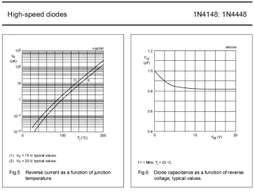
A data sheet for the popular 1N4148 switching diode is shown in Figure 2.11. The 1N4148 is designed for high speed operation required in high frequency signal applications but also finds use in a variety of general purpose applications that do not require very high current or power handling.
Some of the key features include a four nanosecond switching speed, a maximum reverse voltage of 100 volts and a 450 milliamp maximum forward current (with short single pulses as high as four amps being possible). Power dissipation is 500 milliwatts.
Referring to Figure 2.11b, the variation in reverse current with regard to temperature is obvious. This also verifies the “doubles every 10 C°” rule-of-thumb.
4 Cathode is often denoted by a k. This is likely due to the word's Greek root, kathodos.
Figure 2.7
Diode schematic symbol (ANSI).
Figure 2.8
Alternate diode schematic symbol (IEC).
Figure 2.9 DO-204 case.
Figure 2.10 DO-4 case.
Figure 2.11a 1N4148 data sheet. Courtesy of NXP Semiconductors.
Figure 2.11b
[image:36.612.64.428.425.698.2]Figure 2.11c
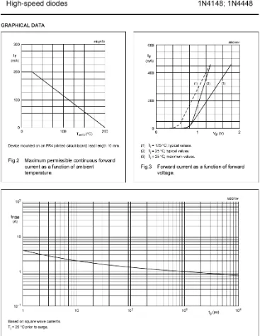
Power derating and permissible pulse amplitudes can be seen in Figure 2.11d. Finally, note the variation in the forward voltage curves due to temperature. As stated previously, for a given current, an increase in temperature results in a lower forward voltage. Also, at room temperature, we see a knee voltage of approximately 0.7 volts.
Figure 2.11d
2.4 Diode Circuit Models
2.4 Diode Circuit Models
One thing is very clear from the characteristic curve of the diode: It is not a linear bilateral5 device, quite unlike a resistor. Consequently, we cannot use the
superposition technique to solve diode circuits unless we have a priori knowledge about it, that is, whether or not it is forward- or reverse-biased. For example, we can imagine a circuit comprised of two voltage sources, resistors and a diode. By itself, one of the voltage sources might forward-bias the diode while the other would reverse-bias it. Obviously, a diode cannot be both forward and reverse-biased at the same time.
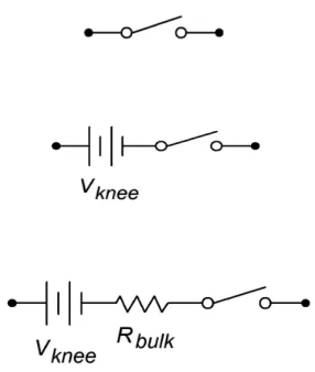
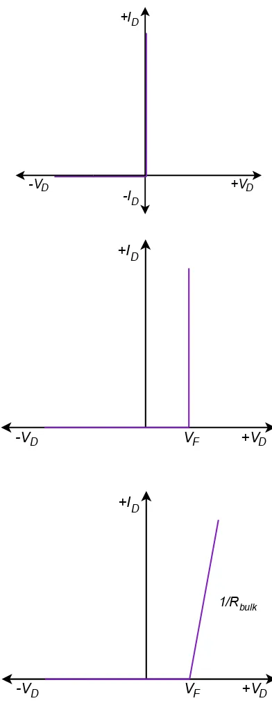
A second problem we face with circuit analysis is the added complexity of the Shockley equation. For speed and ease of computation we find it useful to model the diode with simpler circuit elements. Three diode models are shown in Figure 2.12.
The first approximation is the simplest of the three. It treats the diode as a simple dependent switch: the switch is closed if the diode is forward-biased and open if it is reverse-biased. The second approximation adds the effect of the forward voltage.
Vknee is the “turn-on” potential required to overcome the energy hill. It would be 0.7
volts for a silicon device. The third approximation is the most accurate of the three. A close look at the characteristic curve of Figure 2.4 shows that once the knee voltage is reached, the curve does not transition to a perfect vertical line. Instead, there remains some positive, non-infinite slope. That is, the voltage continues to increase, although modestly, with further increases in current. We can approximate this effect as a small resistive value, Rbulk. The three corresponding I-V plots are
shown in Figure 2.13. Compare these to Figure 2.6 and note the increasing accuracy.
[image:39.612.175.318.285.454.2]5 The I-V plot is not a straight line (linear) and the forward and reverse quadrants are not identical (bilateral).
Figure 2.12
Simplified diode models. Top to bottom: first, second and third approximations,
In many applications the second approximation will yield sufficiently accurate results and we will tend to make greatest use of it. Just remember that these are behavioral models; don't think that there are literally 0.7 volt sources or little resistors in the diodes.
Figure 2.13
I-V curves for simplified diode models.
Top to bottom: first, second and third approximations.
+ID
+VD
-ID -VD
+ID
+VD
-VD VF
+ID
+VD
-VD VF
It should be noted that Rbulk does not represent the “diode resistance” per se, rather, it
models a minimum value. There really is no such thing as a singular diode resistance. We can, however, talk about the effective resistance of a diode in a particular circuit in both DC and AC terms.
The key to understanding this concept is to remember that resistance is a linear function, a straight line on a I-V graph. Therefore, we need to find a straight line “fit” for the diode curve. Two possibilities are shown in Figure 2.14.
The red curve is the diode's characteristic curve (arbitrary current values are shown). For some particular DC circuit, a specific current will flow through the diode which will produce a particular voltage, denoted on the graph as the operating point. If we simply compute the ratio of that voltage to the driving current, we wind up with a resistance. This is the effective DC resistance of the diode under these circuit conditions and is represented by the blue line. That is, the reciprocal of the slope of the blue line is the effective DC resistance. Obviously, if we shift the operating point along the red diode curve, the slope of the intersecting blue line changes and therefore we arrive at a new DC resistance. The higher the current, the lower the effective DC resistance.
Instead of just DC, the diode might see a combination of DC and AC signals. Visualize this as adding a small AC variation on top of the DC. We can imagine the operating point moving along the red diode curve, back and forth about the
[image:41.612.59.477.208.455.2]operating point. If we divide the small AC voltage variation by its associated AC
Figure 2.14
Diode effective resistance for DC and AC.
Diode Effective Resistance
D io de C ur re nt 0.000 0.001 0.002 0.003 0.004 0.005 0.006 0.007 0.008 0.009 0.010