AFIPS
CONFERENCE
PROCEEDINGS
VOLUME 39
1971
FALL JOINT
COMPUTER
CONFERENCE
November
16- 18. 1971
The ideas and opinions expressed herein are solely those of the authors and are not necessarily representative of or endorsed by the 1971 Fall Joint Computer Con-ference Committee or the American Federation of Information Processing Societies, Inc.
Library of Congress Catalog Card Number 55-44701
AFIPS PRESS
210 Summit Avenue Montvale, New Jersey 07645
@1971 by the American Federation of Information Processing Societies, Inc., Montvale,New Jersey 07645. All rights reserved. This book, or parts thereof, may not be reproduced in any form without permission of the publisher.
DATA COMMUNICATIONS
A universal cyclic division circuit ... . Cyclic redundancy checking by program ... .
APPLICATIONS OF COMPUTERS IN EMERGING NATIONS
Development of computer applications in emerging nations ... . Notions about installing and maintaining a population register in Brazil .. .
OPERATING SYSTEMS-SOME MODELS AND MEASURES
The neutron monitor system ... .
A simple thruput and response model of EXEC 8 under swapping saturation ... . Throughput measurement using a synthetic job stream ... '" .. A feedback queueing model for an interactive computer system ... .
TERMINALS
Alcoa picturephone remote information system (APRIS) ... .
Computer support for an experimental PICTUREPHONE® computer system at Bell Telephone Laboratories Incorporated ... . Proposed braille computer terminal offers expanded world to the blind ... .
SIMULATION OF ENVIRONMENTAL DYNAMICS
Numerical simulation of subsurface environment ... ' ... .
Digital simulation of the general atmospheric circulation using a very dense grid ... . Simulation of the dynamics of air and water pollution ... . Programming the war against water pollution ... . Application of a large scale nonlinear programming problem to pollution control ... .
1
9
17
27
31
39
51 57
65
71 79
89
97
105 115
123
A. W. Maholick R. B. Freeman P. E. Boudreau R. F. Steen
A. B. Kamman A. L. Mesquita
R. Aschenbrenner L. Amiot
N. K. N atarajan J. C. Strauss D. C. Wood E. H. Forman G. Nakamura
M. L. Coleman K. W. Hinkelman W. J. Kolechta E. J. Rodriguez N. C. Loeber
IMAGES AND PATTERNS
Parametric font and image definition and generation ... . A syntax-directed approach to pattern recognition and description ... . Computer pattern recognition of printed music ... .
LARGE SCALE INTEGRATION (LSI)
A storage cell reduction technique for ROS design ... . A new approach to implementing high-density shift registers ... . Universal logic modules implemented using LSI memory techniques ... .
COMPUTERS IN MEDICINE-PROBLEMS AND PERSPECTIVES (PANEL SESSION)
Position paper ... . Position paper ... . Position paper ... .
THE USER INTERFACE FOR INTERACTIVE SEARCH (PANEL SESSION)
Chairman's Note .... " ... .
STATE OF THE COMPUTER ART IN BIOLOGY (PANEL SESSION) Position paper ... . Position paper ... . Position paper ... : ... . Position paper ... . Position paper ... .
SIMULATION OF AEROSPACE SYSTEMS
Introduction to training simulator programming ... . The handling qualities simulation program for the augmentor wing jet STOL research aircraft ... . Software validation·of the Titan IIlC digital flight control system utilizing a hybrid computer ... .
r Multivariable function generation for simulations ... .
PROGRAMMING LANGUAGES AND LANGUAGE PROCESSORS Problems in, and a pragmatic approach to, programming language
measure-ment ... . The ECL programming system ... . The "single-assignment" approach to parallel processing ... . MEANINGEX-A computer-based semantic parse approach to the analysis of meaning ... , .... .
135 145 153
163 171 177
195 195 196
197
199 199 200 201 201
203
213
225
233
243 253 263
271
A. J. Frank L. D. Menninga D. S. Prerau
C. K. Tang T. S. Jen K. J. Thurber R. O. Berg
B. G. Lamson C. T. Post, Jr. E. E. Van Brundt
J. L. Bennett
C. Levinthal N. E. Morton R. Nathan W. F. Raub W. S. Yamamato
D. G. O'Connor W. B. Cleveland R. S. Jackson S. A. Bravdica P. Chew J. E. Sanford E. Z. Asman
Law enforcement communications and inquiry systems ... . The Long Beach public safety information subsystem ... .
State criminal justice information system ... . Automated court system ... .
EXPERIMENTS IN ON-LINE DELPHI RESEARCH
Delphi and its potential impact on information systems ... . Technology for group dialogue and social choice ... . Structuring information for a computer-based communications medium ... .
INTERACTIVE CONTINUOUS-SYSTEM SIMULATION IN RESEARCH AND EDUCATION
INSIGHT-An interactive graphic instructional aid for systems analysis ..
An interactive class-oriented dynamic graphic display system using a hybrid computer ... . Hybrid terminal system for simulation in science education ... . BIOMOD-An interactive computer graphics system for modeling ... .
The future of on-line continuous-system simulation ... .
COMPUTER STRUCTURES-PAST PRESENT AND FUTURE (PANEL SESSION)
Position paper ... . Position paper ... . Position paper ... . Position paper. . ... .
COMPUTERS IN SPORTS (PANEL SESSION)
Position paper ... . Position paper. . ... . Position paper ... . Position paper ... . Position paper ... . Position paper ... ' ... .
TWENTY YEARS IN PASSING (PANEL SESSION) (No papers in this volume)
281 295
303 309
317 327 337
351
357 361 369
379
387
395 395 395
397 397 398 399 399
400
J. D. Hodges, Jr. G. Medak P. Whisenand G. Gack R. Gallati R. Baca M. Chambers W. Pringle S. Boehm
M. Turoff T. B. Sheridan S. Umpleby
M. J. Merritt R. Sinclair A. Frank D. C. Martin G. F. Groner R. L. Clark R. A. Bermam E. C. DeLand H. M. Aus G. A. Korn
C. G. Bell A. Newell F. P. Brooks, Jr. D. B. G. Edwards A. Kay
DATA SECURITY IN DATA BASE SYSTEMS
Multi-dimensional security programs for a generalized information retrieval system ... .
for statistical purposes ... . The formulary model for flexible privacy and access controls ... . Insuring confidentiality of individual records in data storage and retrieval
THE APPLICATION OF COMPUTERS TO URBAN PLANNING AND DEVELOPMENT
Integrated municipal information systems: Benefits for cities--Require-ments for vendors ... . Geocoding techniques developed by the census use study ... . Urban COGO-A geographic-based land information system ... .
SELECTED PAPERS IN DISCRETE SIMULATION
Understanding urban dynamics. . . . ... . Bankmod-An interactive decision aid for banks ... . Simulation of large asynchronous logic circuits using an ambiguous gate model ... . Adaptive memory trackers ... .
PLANNING COJVIMUNITY INFORMATION UTILITIES (PANEL SESSION)
Position paper ... . Position paper ... . Position paper ... . Position paper ... . Position paper ... .
COMPUTERS AND THE PROBLEMS OF SOCIETY (PANEL SESSION)
Position paper ... . Position paper ... . Position paper ... . Position paper ... . Position paper ... .
571
579 587
603 609
619
631 639
651 663
669 670 671 671 672
675 675 676 677 677
J. M. Carroll R. Martin L. McHardy H. Moravec M. H. Hansen L. J. Hoffman
S. E. Gottlieb C. C. Smith lV1. S. White, Jr. B. Schumaker
G. O. Barney
W. P. Hoenhenwarter K. E. Reich
S. G. Chappell G. Epstein
B. W. Boehm N. D. Cohen B. Nanus N. R. Nielsen E. B. Parker
spatial dimensions ... . Numerical solution of partial differential equations by associative processing Consistency tests for elementary functions ... .
LABORATORY AUTOMATION
Laboratory automation at General Electric corporate research and
develop-401
411 419
ment... 423
1\1ulticomputer processing in laboratory automation. . . . 435
Enhancement of chemical measurement techniques by real-time computer. interaction. . . 441
The television/computer system-Acquisition and processing of cardiac
catherization data u~ing a small computer. . . .. . . . 455
Cost benefits analysis in the design and evaluation of information systems. . 469
Factors to be considered in computerizing a clinical chemistry department
of a large city hospital. . . . 477
DATA BASE SYSTEMS DESIGN
Integrated information system ... . A machine independent FORTRAN data management software system for scientific and engineering applications ... . Requirements for a generalized data base management system ... .
INTERACTIVE TEXT EDITING SYSTEMS
User engineering principles for interactive systems ... . Computer assisted tracing of text evolution ... .
PLANNING AND DESIGNING OF HIGH PERFORMANCE SYSTEMS Planning computer services for a complex environment ... . A high performance computing system for time critical applications ... .
Effective corporate networking, organization, and standardization ... .
491
501 515
523 533
541 549
561
G. A. Bekey M. T. Ung
P. A. Gilmore A. C. R. Newbery
P. R. Kennicott V. P. Scavullo
J. S. Sicko E. F. Lifshin C. E. Klopfenstein C. L. Wilkins S. P. Perone H. J. Covvey A. G. Adelman C. H. Felderhof P. Mendler E. D. Wigle K. W. Taylor
I. Learnman R. L. Morey M. C. Adams E. Laga
J. C. Pendleton I. Hirschsohn A. C. Patterson IV
W. J. Hansen W. D. Elliott A. Van Dam W. A. Potas
by ANDREW W. MAHOLICK and RICHARD B. FREEMAN
IBM Corporation
Research Triangle Park, North Carolina
INTRODUCTION
Recent innovations in circuit technology have allowed design alternatives that previously would have been economically unsound. LSI technology permits the use of generalized systems containing more logic than the specialized systems used in the past, implemented in unit logic, and at even lower cost. Five years ago an engineer would not have even considered using a cyclic redundancy checking circuit in the manner described here.
Cyclic Redundancy Checking (CRC) is a relatively old technique for use in error detection. W. W. Peterson and D. T. Brown1 wrote a fundamental paper pointing out the great potentialities for cyclic codes in error detection and the requirements for implementing such error detection systems. The specialized serial case, i.e., with one input channel and one output channel, has been extensively studied and is contained in the Peterson2 text. Many related papers, including pioneer-ing efforts on this subject, are contained in a book edited by Kautz.3 Hsiao and Sih,4 Hsiao,5 and Patel6
have concentrated on the generalized case of CRC cir-cuits with parallel multiple-channel inputs and outputs.
The above articles emphasize the use of fixed wiring patterns to implement the error-detection capabilities of cyclic redundancy codes. The hardware would re-quire a complete rewiring to change the polynomial for the cyclic redundancy check. This, in turn, would mean that the circuitry itself would have a limited usefulness because only one type of polynomial could be used within a system at anyone time.
Conventional CRC circuits for a given polynomial and data character size consist of a serial-by-bit shift register with EXCLUSIVE OR feedback circuits in those bit positions which represent a term in the CRC polynomial. Figure 1 shows an implementation for the polynomial, X16+X15+X2+ 1. In a digital data com-munication system, this bit-synchronous scheme must usually be duplicated for each communication line. In
1
communication line multiplexers the logic is sometimes shared, but it is limited to those communication lines using the same CRC checking polynomial.
We shall describe a generalized method for updating cyclic redundancy checking logic at the character level which is capable of operating upon any data character size in conjunction with any checking polynomial of a given length.
RECEIVED OR TRANSMITTED CHARACTER BITS
TO BE INCLUDED. IN eRe ACCUMULATION
2 ),EEDBACK DATA
FIGURE 1 - SIMPLIFIED SERIAllMPlEMfNTATION OF THE POLYNOMIAL, Xf6 • xl5 + x2 + I
Figure 1-Simplified serial implementation of the polynomial
X16+X15+X2+1
We shall describe the device from the point of view of its application in a digital data communication line multiplexer where a variety of CRC polynomials might be employed to service multiple communication lines. However, it should be noted that this device can be used by future terminals as well as by the increasing number of I/O devices (tapes, discs, et al.) which are employing CRC checking.
THE EVOLUTION FROM SERIAL TO PARALLEL
In this section we shall trace the evolution of the polynomial, X8+X5+X3+X+l, from its serial-by-bit
2 Fall Joint Computer Conference, 1971
INPUT DATA SHIFT REGISTER
Figure 2-8implified serial implementation of the polynomial
X8+X5+X3+X +1
the generalized method described later that can process
f
bits in parallel for any arbitrary checking polynomial to generate the CRC character or the syndrome.From Patel,6 we have the required theoretical rela-tionship between the serial-by-bit and parallel-by-character cases. A brief section is reproduced for the convenience of the reader in Appendix A.
Figure 2 shows the conventional serial-by-bit imple-mentation for the polynomial, X8+X5+X3+X+1, to
be used in conjunction with a four-bit data character. Figure 3 shows an equivalent circuit in which re-dundant EXCLUSIVE-OR circuits have been added
,
such that there is one at the input of each stage of the shift register. Those EXCLUSIVE-ORS not required to implement the polynomial have one input connected to a "logical 0" voltage level. Thus, the input coming from a previous shift register stage will pass through asif the EXCLUSIVE-OR circuit were not there, i.e.,
O+X=X.
Figure 4 shows another functionally equivalent cir-cuit. Some flexibility is obtained by the addition of an AND circuit, which controls one input of the EX-CLUSIVE-OR circuit. One input of each AND circuit is connected in common to the feedback path. The other input of each AND circuit may be connected to either a logical 1 or 0 voltage level according to whether or not the corresponding term exists in the polynomial.
Figure 5 shows another step in the evolutionary process. The data is entered parallel-by-character rather
Figure 3-Equivalent implementation # 1 for the polynomial
X8+X5+X3+X +1
Figure 4-Equivalent implementation #2 for the polynomial
X8+X5+X3+X +1
than serial-by-bit. This is accomplished by EXCLU-SIVE-ORing the data character with the corresponding low order bits of the shift register prior to shifting. This may be done since the contents of the shift register will be the same after f-bit shifts on a serial-by-bit basis or if the f-bits are EXCLUSIVE-ORed with the low order stages of the shift register and then allowing the f-bit shifts to occur.
Figure 6 shows the next step in the evolutionary process. Here one row of shift registers has been ~dded for each data bit. For all rows except the first, the input of an EXCLUSIVE-OR circuit in cell position Cn,m is connected to the output of cell Cn - i , m-i, where n is the row number and m is the column number. It is connected there rather than to the cell on its immediate left,
Cn,m-i. We shall shift each row from 1 t04 on a mutually
exclusive basis. When the last row has been shifted, the output of row 4 will be identical to the serial-by-bit implementation after four bit shifts.
In the final equivalent circuit every shift register state is deleted such that all that remains is the com-binational logic as shown in Figure 7. In this version, the only time delay that will be encountered is the propagation delay of the logic elements.
We still need some memory elements, however. We require an OLD CRC REGISTER, a NEW CHAR-ACTER REGISTER, and a NEW CRC REGISTER. The NEW CHARACTER REGISTER and the low
Figure 5-Equivalent implementation # 3 for the polynomial
Figure 6-Equivalent implementation #4 for the polynomial
X8+X5+X3+X +1
order position of the OLD CRC REGISTER are EX-CLUSIVE-ORed together. The outputs of the exclusive or circuits plus the high order positions of the OLD CRC REGISTER are connected to appropriate positions in the first row of the array. The updated CRC remainder will appear at the output of the bottom row and will be set in the NEW CRC REGISTER. The contents of the NEW CRC REGISTER can then be transferred to the OLD CRC REGISTER in preparation for the next iteration.
A POLYNOMIAL REGISTER set to the required bit configuration is used in lieu of fixed wiring to select the polynomial. It offers more than is required for the single polynomial implemented since it will provide for any polynomial of the eighth degree.
THE UNIVERSAL CRC REGISTER
For a practical implementation in a communication multiplexer, the system (Figure 8) uses a memory
de-Figure 7-Equivalent implementation # 5 for the polynomial
X8+X5+X3+X +1
Figure 8-Functional block diagram of universal CRC logic
vice which is addressable via a communication line scanner. The location accessed in the memory for a particular line contains unique line control information including the current CRC value, data character length, and a binary representation of the polynomial associated with that line. Subsequent to the receipt of the transmission line address, the memory will be ac-cessed to obtain specific parameters associated with that address to set the CODE LENGTH SELECTOR (6, 7, or 8 bits), POLYNOMIAL, and OLD CRC registers. The old CRC is the cyclic redundancy check remainder calculated for the previous data characters received or transmitted during the current transmission on the line.
At the same time that the transmission line address is made available to memory, the new data character to be serviced from this line is stored in the NEW CHARACTER register.
When all the parameters associated with the trans-mission line address have been set, the CODE LENGTH SELECTOR, POLYNOMIAL, OLD CRC and NEW CHARACTER registers are gated to the inputs of an array calculator.
4 Fall Joint Computer Conference, 1971
was previously stored. On the next iteration, this data will be the old CRC remainder.
CRC calculation continues in a multiplexed fashion. Each communication adapter invokes the CRC param-eters associated with it by presenting a unique memory address to access the memory. This insures that the proper old CRC, code length, and polynomial are com-bined with the new data character to generate the new cyclic redundancy check remainder.
An alternate approach will be to transmit the cyclic redundancy check following the stop character and allow the cyclic redundancy check and the stop char-acter to pass through the universal cyclic redundancy check generator. The result of this operation would be a data word as an output from the array calculator which represents the syndrome. A non-zero syndrome indicates an error in the received data. However, if the syndrome is zero we know only that the received bit stream is one of the allowable set of transmitted bit streams. It may not be the actual transmitted bit stream. That is, an undetectable error may have oc-curred.
OPERATIONAL CHARACTERISTICS
Figure 9 is a detailed presentation of the input logic of the rectangular array calculator which provides for 6-, 7-, or 8-bit data characters and polynomials of order 16 or less. The POLYNOMIAL and OLD CRC registers are 16-bit registers labeled from 0 to 15 and the NEW CHARACTER register is an 8-bit register labeled 0 to 7. Only the first two rows of the rectangular array are shown in Figure 9.
Each of the registers is always filled from data busses entering these registers such that the right-most binary-bit positions in each of these registers represent data corresponding to the particular polynomial terms, the
Figure 9-Input logic for the rectangular array
old CRC value, and the new data character which is required to update the CRC value. In cases where this data does not fill the entire register, the higher order or left-most bit positions are forced to a binary 0 condition as is shown above each of the registers in Figure 9.
While the logic for the array shown in Figure 9 looks very extensive, it should be noted that this is deceptive, since the logic has intentionally been designed as an iterative structure to make it attractive for large scale integration (LSI). The array could be packaged on one chip, making the large amount of logic involved of little consequence.
The logic shown in Figure 9 performs a relatively complicated mathematical function upon the various register inputs to the array, initially, a modulo-two addition (half summing) occurs between the old CRC and new data character. The result of that addition is then applied to the array calculator. The array calcu-lator operates in a manner so as to duplicate mathe-matically the results which might be obtained by serial feedback approaches to CRC generation as previously shown.
The circuitry within the array has its various anal-ogies to serial feedback shift register implementation. For example, the vertical lines such as line 1 in Figure 9 represents a single feedback point in an analogous serial feedback approach to CRC generation (Line 1 in Figure 1). The vertical line represents the presence ("I") or absence ("0") of a term in the chosen cyclic check polynomial. For instance, the polynomial
X16+X15+X2+1 used in Binary Synchronous
Communi-cation would be represented with "I's" in positions 15, 2, and 0 (1 =Xo) of the POLYNOMIAL register. In
effect, there is always a high order term (16 in this case) which necessitates the initial modulo-two addition.
To determine the right-justified positions in the POL YNOMIAL register for polynomials of degree less than 16, it is necessary to multiply the polynomial by
x raised to the power (16-(degree of polynomial)). For instance, the polynomial X6+X5+ 1 would be
im-plemented as though it were X(16-6) (X6+X5+ 1) =
X16+X15+XlO and "ones" would be placed in positions 10
and 15 with position 16 implied. LRC for 8 b t codes (x8+1) would te implemented as X (16-8) (x8+1) = X16+X8 with a "one" in position 8.
data within the serial shifting network. A similar changing of data occurs in the transmission between one cell element and another if the data on the intermediate feedback line and the line from the polynomial register are of the proper values. The output ("I" or "0") of a given cell is equal to the output of the cell diagonally above and to the left of it unless it is reversed by the coincidence of a logical "one" on both the vertical line, and on the horizontal line associated with the position.
THE ARRAY AND ITS OPERATION
Certain machines might interface the array in a dif-ferent fashion than shmvll in Figure 9, i.e., the CRC polynomial select register might be replaced by perma-nent wiring in a terminal application, or the output assembler (described later) might be reduced or elimi-nated if only one data character length exists.
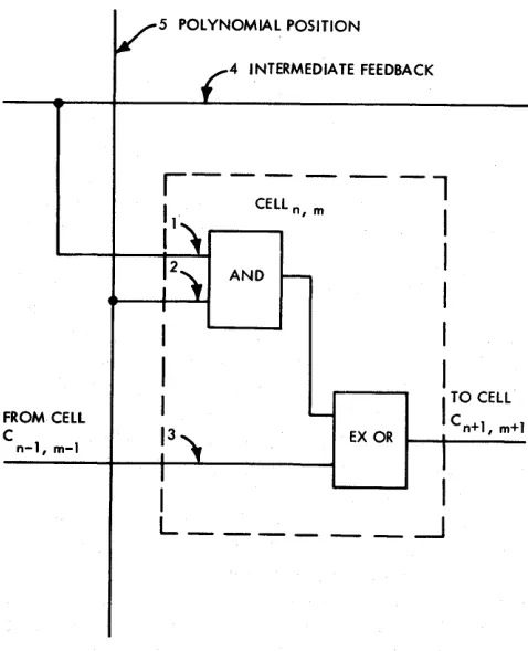
The array consists of replicas of the simple circuit shown in Figure 10. The cell is shown enclosed in the dotted line labeled cell Cn,m on Figure 9. Each cell ele-ment has three inputs. The first, 1, is connected to a line 4 carrying signals representing the binary value for the intermediate feedback within the array calculator. The second input, 2, is connected to a line 5 which has
FROM CELL
C n-l, m-I
5 POLYNOMIAL POSITION
4 INTERMEDIATE FEEDBACK
, - - - 1
I .
CELL n, mI
11
AND
I
I
I
I
I
TO CELLCn+1, m+l
EX OR
I
I
L _ _ _ _ _ _
~Figure H}-Logic diagram for a standard cell of the array
binary information representing the binary value of a given single bit position within the polynomial, and is connected directly to the POLYNOMIAL REGISTER. A third input, 3, is a connection to a cell which is diag-onally upward to the left of the array. Specifically, Cell Cn,m has its third input connected to the output of cell Cn-I,m-I, where n designates the row number and
m the column number.
For the cells in the leftmost column, there are no positions diagonally upward to the left. Therefore, the third input to the cell is wired permanently to a voltage source having a binary value of O.
The cell elements along the first row of the array have a slightly different characteristic than the other cells of the array because the third input to each cell cannot be connected to the cell element diagonally up-ward to the left within the array since no such element exists for those in the first row. For cell element Co,o, cell element row 0 and column 0, the third input is wired to a binary 0 voltage level. For cell element CO,I, the cell element in row 0 and column 1, the third input is connected to bit position 0 of the OLD CRC register. Subsequent cells in row 0 have their third input con-nected directly to the OLD CRC register up to and including cell CO,7.
For cells CO,g to cell CO,IS, the third input to each cell is wired in a different manner than for the other cells within the row. Cell CO,IS provides a good example. The third input to this cell is connected to EXCLU-SIVE OR circuit 6. The inputs to EXCLUEXCLU-SIVE OR 6 are connected to bit position 6 of the NEW CHAR-ACTER register and to bit position 14 of the OLD CRC register. Similar wiring exists for the other array elements CO,8 through CO,I4.
The intermediate feedback signal from EXCLU-SIVE OR 7 is connected to the first input to each of the cell elements in row
o.
The intermediate feedback signal is generated by EXCLUSIVE OR circuit 7. The inputs to EXCLUSIVE OR circuit 7 are connected to bit position 7 of the NEW CHARACTER register and tobit position 15 of the OLD CRC register.PROVISION FOR VARIOUS CODE LENGTHS
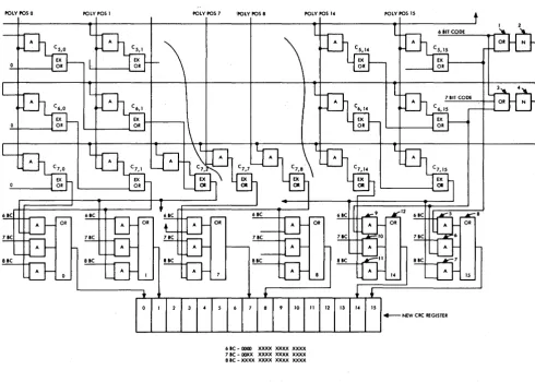
[image:13.613.48.287.419.714.2]6 Fall Joint Computer Conference, 1971
POLY POSO POLY POS I POLY POS 7 POLY POS 8 POLY POS 14 POLY POS IS
10 II 12 13 14 IS
+--NEW eRe REGISTER
6 Ie - 0000 XXXX XXXX XXXX 7 Ie - OOXX XXXX XXXX XXXX 8 Ie - XXXX XXXX XXXX XXXX
Figure ll-Output logic for the array
code of degree 7 would extend from positions 9 to 15 in the POLYNOMIAL register. Positions 0 to 8 would be set to zero. This method appropriately tr~cates the "width" of the array.
However, the "depth" of the array must also be truncated in accordance with the character length. Each row of the array represents a serial shift of one bit. Thus, for a 6-bit code, using an array designed for eight bits, the desired answer is present and properly aligned at the outputs of the sixth row. However, be-cause of chip layout limitations, it is not practical to bring out indeplmdent outputs from each of several rows.
Thus, a compromise is struck by degating the inter-mediate feedback path to lower rows, which results in a single right shift of the answer for each such row. Note that the right-most bits wrap around the bottom right side, appearing as the outputs of the right-hand positions of the second row up (for a 7 -bit code) or subsequent rows for shorter codes. Thus for multi-length systems it will be necessary to assemble for proper alignment some time before the NEW CRC be-comes the next OLD CRC. See Figure 11. The resultant
alignment is as shown at the bottom of Figure 11 for 6-, 7-, and 8-bit code lengths and 12-, 14-, and 16·degree polynomials, respectively.
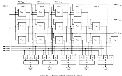
[image:14.615.64.555.86.436.2]POLY 0
0
0
0
6 B1T CODE 7 B1T COQE 8 B1T CODE
FROM C. 0 FROM C. 1
l
POLY 1l
POLY 2~ C5,0 ~ ~ C 5,1
-L
L
~ C 6,0
---
~ C 6,1L
L
-
C 7,0-
C 7,1A
I
OR+
TO NEW CRC 0I I
FROM C. 2
L
POLY 3 f - - - ~ C 5,2-A
' -I
-L
~ C6,2
-
..-L
-
C 7,2oa
OR+
TO NEW CRe 1
I I
FROM C
I
POLY. POLY 5 4,15-
I - - - C5 ,3 -' --FROM C
l
L
5,15
- ..-- C 6,3 - ~ C 6,4
-
~ r-l
L
L
FROM C 6,15-
C 7,3 t--
C7,4 t- ' - - - C 7,5'---4~
-
~A
OQ
AMMo
OR
+
TO NEW CRC 2
1 I
OR+
TO NEW CRe 3
I
I
OR+
TO NEW CRC 4
I
Figure 12-Alternate output logic for the array The output of Cell GS,IS is propagated to AND circuit 5.
When a 6-bit code is selected, a positive voltage will appear on the second input to AND circuit 5. The data appearing on the output of cell Gus would then be transmitted via AND circuit 5 or OR circuit 8 and on to bit position 15 of the NEW CRC register.
Bit position 14 of the output is gated from cell ele-ment G6,IS to AND circuit 9 when a 6-bit code is indi-cated. AND circuit 9 has an output connected to OR circuit 12 whose output is connected to bit position 14 of the NEW CRC register.
Cell element Gus provides the output for bit posi-tion 13 of the NEW CRC register when a 6-bit code is being operated upon. This is accomplished by gating circuitry not shown. The other bit positions of the NEW CRC REGISTER would be filled from data from cell elements in row 7 of the array in a similar manner to that described for bit position 13 in the NEW CRC REGISTER when a 6-bit code was being transmitted. Inthe case where the new character contains eight data bits, each of the outputs of the eighth row of the array calculator would be connected directly to the NEW CRC register via appropriate switching circuits and no compensation for the shift in the array network would be necessary.
The gating circuitry above-mentioned in connection
with Figure 11, is particularly adapted to LSI cir-cuitry because the output gating occurs from elements of the network which are on the peripheries of the rec-tangular array calculator. With the above scheme, the array could easily be placed in a single chip and all wiring connections can be made to points within the array without crossing any internal connections.
The advantage to the above-shown output gating is that additional wires from the outside of the array are not necessary to connect to interior points within the array. Where such wiring problems do not exist, a simpler approach to the outputting is shown in Figure 12. This logic is a simple AND-OR assembler where row 5,6, or 7 is selected for gating into the NEW CRC register, depending on whether the code length is 6, 7, or 8 bits, respectively. This assembly function can be considered as part of the array element and can there-fore be extended throughout the array to provide for any code length.
ACKNOWLEDGMENT
[image:15.613.51.556.88.405.2]8 Fall Joint Computer Conference, 1971
REFERENCES
1 W W PETERSON D T BROWN Cyclic codes .for error detection
Proceedings of the IRE pp 228-235 January 1961
2 W W PETERSON Error correcting codes MIT Press 1961
3 W H KAUTZ
Linear sequential switching circuits Holden-Day Inc 1965
4 M Y HSIAO K Y SIH
Serial-to-parallel transformations of feedback shift reg1:.'1ter circuits
IEEE Transactions on Electronic Computers VOL EC-13 pp 738-740 December 1964 5 M Y HSIAO
Theories and applications of parallel linear feedback shift register
IBM TR 1708 SDn Poughkeepsie March 1968 6 A M PATEL
A multi-channel eRC register
AFIPS Conference Proceedings Vol 38 pp 11-14 Spring 1971
APPENDIX A
The following is reproduced from Pate16 :
In this section, we develop the mathematics for ob-taining a multi-channel CRe register that can process
1
bits in parallel to generate the eRe character or the syndrome. One shift in the parallel circuit is equivalent to1
shifts in the corresponding serial eRe register. The number1
is a positive integer, smaller than the degree r of the checking polynomial.G (x) denotes the checking polynomial, often called the generator polynomial. We use the following no-tation:
The state vector Xt=(xo, Xl, ... Xr-l)t denotes the con-tents of the eRe register at time t. T denotes the companion matrix of.the polynomial G(x), correspond-ing to the serial eRC register connections. Let Zt denote the data bit entering the serial eRe register at time t.
Then the shifting operation of the serial eRe register is given by the (mod-2)_ matrix equation
Xt+1=XtTEBztG (2)
where G is the vector (Go, GI , G2 . . . Gr- 1), and T is
given by:
0 1
0 1
T= 1 (3)
0 1
Go G1 G2 Gr-1
Suppose that Zt, Zt+l, ... Zt+f-l are the
f
data bits (a byte) entering successively into the serial eRe register during thef
consecutive shifting operations. The contents of the eRe register at the end of1
shifts is denoted by the vector Xt+f . Using Equation 2itera-tively,
1
times, one can obtain:Xt+!=XtTfEBZtGTf-lEBZt+1GTf-2EB . . . Zt+f-lG (4)
Here Ti is the jth power of the matrix T. Let Z t denote the input data sequence, as follows:
Zt= (Zt+!-l, Zt+f-2, ... , zt+1, Zt)
Let D denote the following partitioned matrix:
G
GT
D= GT2
GTf-1
(5)
Note that the vectors G, GT, GT2, ... GTf-1
repre-sent the contents of the serial eRe register a.s the vector G is shifted
1-1
times.Then, Equation 4 can be rewritten as:
Xt+!=XtTfEBZtD (6)
The sequential circuit realizing Equation 6 has the property that with the input byte Zt (1 bits in parallel), it changes from state Xt toXt+! in a single shift. This
by P. E. BOUDREAU and R. F. STEEN
IBM Corporation
Research Triangle Park, N.C.
INTRODUCTION
Recent advances in the use of mini-computers as control elements of a computer complex and as in-telligent terminals! are indicative of a trend toward relocation of certain hardware functions to micro-program or machine level micro-program. One such function which is a particularly good candidate, for various reasons, has already been moved into program in several machines (e.g., IBM System 360/25 Integrated Communication Adapter2 and the IBM 11303). This function is error control using an error detection Cyclic Redundancy Check (CRC). A CRC is a variable length shortened cyclic code in which a message is a code word if, and only if, the message polynomial M(x) is divisible by the generator polynomial G(x).
Error detection and correction codes have been studied extensively for more than 15 years. The most comprehensive references,4,5 as well as the majority of papers written in the area, measure the encoding and decoding complexity in terms of the cost of hardware and the time for decoding. With some notable excep-tions,6,7 very little attention is given to the problem of encoding and decoding using machine level or micro-instructions. However, in some cases such as the Berlekamp algorithm3 for BCH codes, it may very possibly be easier to write a program for certain steps of the decoding procedure than to design hardware. Programmed error correction is especially· appealing for use with high rate codes when error probabilities are low, since, in this case, a major portion of the correction process need only be performed when errors actually occur. Allocation of a significant amount of hardware for these relatively infrequent events is expensive. Further-more, rapidly advancing memory technology helps to make program-controlled devices not only economically feasible but attractive.
9
One part of the problem is addressed in this paper.
It is the problem of encoding or generating check bits. The solution, however, also applies to the decoding problem for error detection codes of this type. A similar approach, based on the properties of the companion matrix, has been used for parallel hardware devices. 8,9 With this approach, efficient and attractive programs can be developed for software or firmware. Subroutines developed here require as few as six instructions with sequential instruction execution to update a 16-bit remainder for eight new information bits. A program directly simulating a shift register would require at least three instructions (EXCLUSIVE OR, SHIFT, and BRANCH) per bit, or 24 instructions for an eight-bit update.
MATRIX APPROACH TO CYCLIC CODES
In this section, we review the relationship between multiplication by the companion matrix and poly-nomial division used to generate a code word. We then generalize the operation to an m-bit character-by-character operation developing a matrix equation to update the calculated redundancy m bits at a time. The
appendix will be helpful to those familiar with the shift register in order to further justify the connection be-tween the shift register operation and the matrix multiplication.
10 Fall Joint Computer Conference, 1971
o
1°
o
o
0 1°
G=
o
0°
1Then, if we let b(l) =ik- I be the first information bit (the k-lth coefficient of l(x» and b(k) =io be the
last information bit, it is clear (see the appendix or Reference 7) that the remainder R can be calculated iteratively using the following formula:
A (t+ 1) ={A (t) +[0,0, ... ,0, b(t+ 1)]}·G (1)
and setting R=A(k). It should be noted that A(t)
represents the remainder of xhlt(x) divided by G(x) which is the calculated redundancy after the first t information bits, It(x), have been taken into account.
We now define B(t+ 1) = [0, 0, ... , 0, b(t+ 1)] and
rewrite Equation (lor A2) as
A(t+l) =[A(t)+B(t+l)]G. (2)
Equation (2) is the basic matrix description of the polynomial division process (circuit function) on a bit-by-bit basis. The advantage of the matrix approach is realized when one extends it to a multibit or char-acter level. We can do this for m bits-per-character as
follows, assuming m ~ h. Repeated use of Equation (2) yields:
A(t+m) =[A(t+m-l)+B(t+m)J·G
= {[A(t+m-2)+B(t+m-l)}G
+B(t+m)} ·G
m
=A (t) ·Gm+
:E
B(t+j) • Gm-i+l. (3)i=1
Equation (3) expresses the remainder at time t+m in
terms of the remainder at time t and the next m input
bits b(t+l), b(t+2), ... , b(t+m). This equation can
be put into a better form by using the "shifting" property of the companion matrix G.
A (t+m) =A (t) ·Gm
+[0,0, ... ,0, b(t+m), b(t+m-l), ... , b(t+l)}Gm.
(4)
If indeed we are operating with m bits per character and
A (t) is the remainder after some character has been sent, then A(t+m), given by Equation (4), is the
remainder after the next character has been sent and
b(t+m), b(t+m-l), ... , b(t+l) is the bit string of
length m representing that next character, where b(t+l) is the first bit sent.
Since we will be using this from now on, it is con-venient to make a slight change of notation. We define
as the remainder after the jth character, and
as an h component vector where
Co.h CI.h C2.i· .. Cm-l.i
is the bit string of length m representing the jth
char-acter and Cm-I.i is the first bit of the character
trans-mitted. That is
and
for i=O, 1, ... , h-l
Co.i=b(t+m)
CI.i=b(t+m-l)
Cm-I.i=b(t+ 1).
With this notation Equation (5) becomes the char-acter-by-character version of Equation (2)
(5)
This equation expresses the remainder after j
+
1 characters as a function of the remainder after j char-acters and the j+
1st character for m ~ h bits per character. It is the fundamental result which we apply below.MATRIX IMPLEMENTATION OF CYCLIC CODES
This matrix description of cyclic checking leads directly and intuitively to several different programmed checking implementations. It is this feature which makes the approach valuable. Since instruction sets, core availability, and instruction execution times vary widely, three approaches will be described.
comments should clearly indicate the general nature of the operation on each line of code. It is assumed that there are four 16-bit registers which are available to the programmer. These are represented by the APL vector variables RA, RB, and RC with the fourth being the base register which is used for the return branch to the main program. In APL, RA[1 ;J represents the high order byte of register RA and RA[2;J represents the low-order byte of the same register. The storage area for tables is represented by the matrix SA which is as large as necessary.
Although we have assumed a 16-bit data path for the three examples, it is easy to write similar subroutines for an eight-bit ALU by partitioning the G8 matrix in a different manner. We will use the terms, "byte" and "halfword" to mean eight and 16 bits respectively. In general, our methods below are iterative schemes for finding the remainder using the recurrence relation-ship
AHI
=
[Ai+Ci+lJGm.For simplicity we define what we call a "working remainder" W i+l,
= [aO,h •.. , ah-m-l,h (ah-m,iEBCO,i+l) ,
••• , (ah-l,i EB Cm-l,Hl)
J
Basically, our problem is to find AHI given WJ+l and
Gmusing
AH1
=
Wi+1Gm.Since WH1 is a binary vector of length h, it can take
no more than 2h values. The following methods, called the "one-256-halfword-table look-up," the "two-32-halfword-table look-up," and the "binary summation" method, are various ways to perform this job.
Purely for ease of notation, we now fix the values of hand m. We will let the number of parity bits be 16(h
=
16) and the number of bits per character be eight (m=8). Substitution in (5) gives us the funda-mental equationwhere
Wi+! = Ai+Ci+l
Ao= [0,0,0, ... ,0, OJ
Ci=[O, 0, ... ,0,CO,hCl,h ••• ,C7,iJ
are all 16-bit vectors, and
(6)
G8
=
the companion matrix raised to the 8th power.We note again for emphasis that C7,j is the first bit of
the jth character while the j = 1st character is the first character transmitted or received.
One-256-halfword-table look-up method
This is a simple one-table look-up method which requires a significant amount of storage and frequently will be impractical for codes with more than eight bits-per-character. However, it embodies most of the basic ideas of the matrix approach and is a good starting place. In an instruction set with the logical EXCLUSIVE OR operation, the forming of WH1 is trivial. The next
stepjs to find Ai+! which can be found by multiplying Wj+1 by G8. This can be done very rapidly by table
look-up. Rather than blindly storing all 216 halfwords
which can result from this operation, we notice that G8
has the form
0'=
[OiT
Thus WH1G8 can be written
Wi+l(L)XEBWH1(H)[0
I
I]where Wi+1(H) is an eight-bit vector comprising the high-order eight bits of W H1 and Wi+l(L) represents the
low-order eight bits of WH1. If byte operations are
available, the product WH1(H). [0
I
I] is simply movingthe byte from the high-order half of a 16-bit register to the low-order half. The second instruction in Table I performs this operation. The second product above requires a table look-up for one of 256 halfwords representing all possible values of WH1(L) ·X. This is
done in instruction four after the program has shifted the address left one bit in order to force the address to a halfword boundary. The table is assumed to be located on a 512 byte boundary. Its address is stored in the seven low-order bits of the high-order byte of the RB register. The two results are EXCLUSIVE ORed together in the fifth instruction and the table address is restored in the last instruction before the return branch. Table I shows the program which will update the CRC for a full eight-bit character.
This is called the one-table, one-step look-up method.
It is very fast but may be impractical because of the quantity of core required.
Two-32-halfword-table look-up method
12 Fall Joint Computer Conference, 1971
TABLE I-Subroutine Using One-256-Halfword Look-up Initial conditions for all subroutines:
Register RA contains the old CRC, Ai
Register RB2 contains the new character, Ci+1•
Final conditions for all subroutines:
Register RA contains the new CRC~ Ai+1'
V CRC1 EXCLUSIVE OR RB2, RA2
MOVE RB2, RA1
[1] RB[2;] ~ RB[2;] ~ RA[2;] Form Wi+1 (L)
Form Wi+1(H)[0 I I]
Form address SHIFT LEFT RB, 1
LOAD RA, RB
EXCLUSIVE OR RA, RC ROTATE LEFT RB, 15 BRANCH RETURN
write G8 as
[2] RC[2;] ~ RA[l;]
[3] RB ~ ((15p1), 0) /\ 1cf>(l6pRB)
[4] RA ~ 28 p(16p2) T SA[2 J.. RB]
[5] RA[2;] ~ RA[2;] ~ RC[2;]
[6] RB ~ 2 8 p(15cf>RB)
V
Load Wi+1(L)X
Form Ai+l
Reset address Return
G8=
[~]
YIZ
called PTYRC, the even parity of register RC. Looking back to the defining equation
Aj+l= [Cj+l+A j ]-G8= Wj+l-G8.
Here, the Y and Z matrices are four by 16 binary matrices and Wj+l(L) is broken into two four-bit vectors
Wj+l(LL) and Wj+l(LH). Thus, the new calculation
becomes
Aj+l= Wj+1(LH) -YEe Wj+l(LL) -ZEe Wj+1(H) -[0
I
J].Each of the products is a 16-bit row vector. The program now requires two look-up operations for the first two terms and a byte move for the last term. All three terms must then be EXCLUSIVE ORed together. The program is shown in Table II.
Binary summation method
Finally, it is possible to perform this whole operation without tables. This is done by performing the matrix multiplication by program rather than by table look-up. This requires a parity test as a condition on the branch instruction, however. This branching condition will be
Let Dk = [dO,k' d1,k, ••• , d l5 ,k] be the kth column of
G8. Then the high-order position of the new remainder
Aj+l is given by
15
aO,j+l =
L:
d i ,l-Wi,j+li=O
which is operationally the same as ANDing the first column of the matrix G8 with the working remainder
Wj+! and finding the even parity of the result. This
parity is the value of aO,j+l. Similarly, we can find
the remaining bits by ANDing Wj+l with each
column Dk+1 and find the even parity to determine
ak,j+l 0 ~ k ~ 15.
15
ak,j+l
=
L:
d i ,k+l- W i,j+li=O
This operation can be carried out in a program as illustrated in Table III.
The program shown here requires more than 80 words
TABLE II-Subroutine Using Two-32-Halfword Look-up
V CRC2 EXCLUSIVE OR RB2, RA2
MOVE RA2, RB2 AND RB2, H'FO' ROTATE LEFT RB2 LOAD RC, RB
EXCLUSIVE OR RC2, RA1 MOVE RB2, RA2
AND RB2, H'OF'
EXCLUSIVE OR RB2,H'1O' ROTATE LEFT RB, 1 LOAD RA, RB
EXCLUSIVE OR RA, RC BRANCH RETURN [1] [2] [3] [4] [5] [6] [7] [8] [9] [10] [11] [12] V
RB[2 ;]~ RB[2;] ~RA(2;]
RA[2 ;]~ RB[2;]
RB[2;]~RB[2;]/\ 1 1 1 1 0 0 0 0 RB[2 ;]~ cf>RB[2;]
RC~2 8 p(16p2) TSA[2+2J.. 16pRB]
RC[2 ;]~ RC[2;] ~RA[l;]
RB[2;]~ RA[2;]
RB[2;]~RB[2;]/\O 0 0 0 1 1 1 1
RB[2;]~RB[2;]~0 0 0 1 0 0 0 0 RB[2 ;]~ 1cf>RB[2 i]
RA~2 8 p(16p2) TSA[2+2J.. 16pRB]
RA~RA~RC
Form Wi+1 (L)
Save Wi+1 (L)
Mask address Form address Load Wi+1(LH)Y
W i +1(H)[O I]E9 Wi+1(LH)Y
Get Wi+1(L)
Form address Form address Form address Load W i +1(LL)Z Form Ai+l
TABLE III-Subroutine for Binary Summation Method
V CRC3 EXCLUSIVE OR RB, RA
LOAD RA, ZERO
[1] RB~2 8 p(16pRB) ~(16pRA)
[2] RA~2 8pO
Form Wi+1 Set Ai+1 to zero
Load Dl
LOAD RC, Dl [3] RC~SA[1 i]
AND RC, RB [4] RC~2 8 pRC/\(16pRB) Calculate D1Wi+l
Branch if aO.i+l =0 Set aO.i+l = 1 BRANCH [7], PTRC
EXCLUSIVE OR RA, H'8000' LOAD RC, D2
[5] ~(~/(1, 16pRC»/SECONDBIT [6] RA[li]~RA[li]~1 000 0 0 0 0
[7] SECONDBIT:RC~SA[2;] Load D2
ANDRC, RB [8] RC~2 8 pRC/\ (16pRB) Calculate D2Wi+1
Branch if al.i+l =0 Set al.i+l = 1
BRANCH Ill], PTRC EXCLUSIVE OR RA, H'4000'
[9] ~(~/(1, 16pRC»/THIRDBIT [10] RA[li]~RA[li]~O 1 0 0 0 0 0 0 And so on for the third through the 15th bits.
LOAD RC, D16 AND RC, RB
[12] SIXTEENTHBIT:RC~SA[16i]
[13] RC~2 8 pRC/\(16pRB)
Load Dl6
Calculate D16Wi+1 Branch if a15.i+1 =0 Set aI5.i+l = 1
Return BRANCH [16], PTRC
EXCLUSIVE OR RA, H'OOOI' BRANCH RETURN
[14] ~(~/(1, 16pRC»/OUT
[15] RA[2;]~RA[2i]~0 0 000 0 0 1 [16] OUT:~O
of storage. However, a reduction in the storage require-ment is possible by forming a loop to calculate the 16 binary sums. Further reduction is also possible when a specific polynomial is chosen and a combination of this and other schemes is used. For example, using G(x) =
X16+X15,+X2+ 1, the number of instructions can be
reduced to less than 20, making this method com-petitive with the other two given here. The key to this method is the branch instruction which tests the condition of the parity of the 16 bits in the accumulator. This is the last of the three matrix-oriented methods to be discussed and generally requires less core storage and more execution time than the previous two.
Other methods which partition the G8 matrix in
other ways are possible and may be better in specific cases.
SUMMARY
Using a matrix description of the operations required to generate the check bits in a cyclic redundancy error-detection scheme leads to new approaches to the soft-ware implementation problem. Certain variations are in use today and have proven to be superior to direct shift register simulation programs in most cases. With an apparent increase in programmable terminals and multiplexers, such approaches are likely to become even more important in the future.
REFERENCES
1 W L SCHILLER R L ABRAHAM R M FOX A VAN DAM
A microprogrammed intelligent graphics terminal IEEE Transactions on Computers Vol C20 No 7 1971
2 A W MAHOLIC H H SCHWARZELL Integrated microprogrammed communications control Computer Design November 1969
3 IBM 1130 synchronous communications adapter subroutine SRL File 1130-30 Form C26-3706-4 IBM Corporation White Plains New York
4 W W PETERSON Error-correcting codes
The M.LT. Press Cambridge Mass 1961 5 E R BERLEKAMP
Algebraic coding theory
McGraw-Hill Book Company New York 1968 6 I B OLDHAM R T CHIEN D T TANG
Error detection and correction in a photo-digital storage system
IBM Journal of Research and Development Vol 12 No 6 1968
7 R T CHIEN
Burst-correcting codes with high-speed decoding
IEEE Transactions on Information Theory Vol IT-IS No 1 January 1969
8 M Y HSIAO K Y SIH
Serial to parallel transformation of feedback shift register circuits
IEEE Transactions on Electronic Computers Vol EC-13 pp 738-740 December 1964 9 A M PATEL
A multi-channel CRC register
AFIPS Conference Proceedings Vol 38 pp 11-14 Spring 1971
10 K E IVERSON A Programming Language Wiley New York 1962
APPENDIX
14 Fall Joint Computer Conference, 1971
o
1
o o o o
o o
J
o o
J
o o o
J
o
J
o o o o
J
o
Figure Al-An elementary shift register
INITAL STATE STATE 1 STATE 2 STATE 3 STATE .. STATE 5
register on a bit-by-bit basis can be written in terms of matrix operations on vectors. Using this approach, it is possible to justify the several table look-up software schemes which are developed in the main text.
A feedback shift register is a device which stores bits in a serial string and is capable of shifting the string one bit at a time. There may be EXCLUSIVE OR and AND gates associated with the shift register which will operate when a shift takes place. The structure of a shift register is shown in Figure AI. The bit storage positions are indicated by a box (D) and the EX-CLUSIVE OR gates are indicated by the "E9." If
the storage positions are denoted as shown, we can illustrate the operation by assuming that bit positions 1, 2, and 3 contain zero and that a one bit is placed on the "IN" lead. A single shift of the register by a clock pulse (not shown) will cause the "IN" to be EXCLU-SIVE ORed with the feedback from position 3 ~nd
placed in position 1. Thus position 1 = 1 (1 E9 0 = 1) . Now, let us assume that "IN" is set to zero and then another clock pulse occurs. Position 3 E9 "IN"
=
0 is placed in position 1. Position 1 E9 position 3 (1 E9 0=
1) is placed in position 2.A general shift register which performs division by
is shown schematically in Figure A2. The AND gates are represented by the" 0." Although the output does represent the quotient, of major interest to us is the
Figure A2-A general division shift register
contents of the shift register which is the h bit remainder R(x) =rO+rlx+··· +rh_Ixh-1
of the bits shifted in at any time. Thus, if we shift information bits
lex) =io+ilx+·· ·ik_IXk- 1
into the shift register, highest degree coefficient first, we will have the remainder of lex) after all k bits have been entered. However, we would prefer to have the remainder of xhl(x) rather than the remainder of lex) so that we may append the remainder bits directly to the information. One way to do this would be to shift the shift register h times after I (x) has been entered. However, this represents wasted time since we can wire the shift register differently in order· to cause it to "pre-multiply" by Xh. This shift register is shown in
Figure A3, and the remainder at time l will be denoted by the polynomial A(x, l). After shifting lex) into this circuit, the remainder R(x) of xhl(x) divided by G(x) will be contained without further shifts; that is, A(x, k) =R(x). If R(x) is appended to xhl(x) , a code word will be formed (R(x) +xhl(x». At the receiver, exactly the same circuit or program may be used to determine whether the received block is a code word.
In order to further illustrate the operation of the shift register, it is possible to develop a set of functional relationships between the bits that have entered the shift register and the contents of the register. These are the circuit equations for the shift register.
Let the bits in the shift register (Figure A3) at time
t be represented by
ao(l), al(l), a2(l), ... , ah-l(t)
where ao(t) is the leftmost bit in )the shift register. We will also denote the bits which are shifted into the shift register as b(l). That is, the contents of the shift register at time T include the effects of all b (t) for
1
<
t ~ T. Since the bits come at discrete times, bothI (x)
b(t+!)
o
x position x 1 position x h-2 position xh-J
position
Figure A4-Development of circuit equations from the pre-multiply shift register
t and T are integers. Figure A4 may help the reader visualize this operation. From the figure, we can write the circuit equations directly.
ao(t+l) =b(t+l) EBah-l(t)
al(t+l) =ao(t) EBgI[b(t+l) EBah-l(t)]
a2(t+l) =al(t) EBg2[b(t+l) EBah-l(t)]
ah-2(t+l) =ah-3(t) EBgh-2[b(t+1) EBah-l(t)]
ah-l(t+l) =ah-2(t) EBgh-l[b(t+l) EBah-l(t)]
(AI)
Since we set the register to zero before beginning to calculate the remainder, we have the initial conditions
With these we can calculate any ai (T) given the
b (t) (0
<
t::::; T) and the generator polynomialG(x) = 1 +gIX+g2X2+ ••• +gh_IXh-I+Xh.
These circuit equations will be used in the development of the matrix equations which are the subject of the main section.
In order to develop a matrix approach to the genera-tion of a set of parity or check bits, we define a vector which consists of h binary components and represents the bits in the shift register at time t as defined above:
N ext, we define G to be the companion matrix of the polynomial G (x) as shown in the main text.
. From the circuit equations (AI), it is apparent that
A (t + I) = [ao (t + I ) , al ( t + I ) , a2 (t + I ), 0 0 0 , ah-l (t + I) ]
=[0, ao(t), al(t) , 0 0 0 , ah-2(t)]
+[0,0,000,0, b(t+l) EBah-l(t)].G.
Equation (A2) below follows immediately if one merely observes that
[ao(t), al(t), 0 0 0 , ah-2(t) , O}G
=[0, ao(l), al(t), 0 0 0 , ah-2(t)].
A(t+1)={A(t)+[0,0, ooo,O,b(t+I)]}·G. (A2)
by ALAN B. KAMMAN
Arthur D. Little, Inc.
Cambridge, Massachusetts
INTRODUCTION
The purpose of this paper is to explore a series of guidelines which will help identify attractive computer applications in emerging countries. We will examine areas of development from the standpoints of natural resources, labor intensive industries, public and private services. Then we shall explore levels of development in communications, education, high technology and the financial commitment of a nation. We shall examine the computer applications from a cost versus benefits view-point, and finally discuss a feasibility planning study.
A basic assumption throughout this paper, is that there is no such thing as a "model" or "average" developing country. Nor is there such a thing as an Haverage" computer application. Each emerging nation and each application must be explored and related as a separate case.
AREAS OF DEVELOPMENT
Natural resources
Developing countries can often be placed into one of two major categories; those that primarily depend on natural resources for their economy, and those which depend on labor intensive industries. From the stand-point of natural resources, the subcategories include applications such as agriculture, fuels, minerals, water and power. South American copper and coffee coun-tries, West Indian fruit companies, Near East oil producing countries provide relevant examples.
Computers often enter first into natural resource countries with high technology industries (to be dis-cussed in more detail later) such as in oil producing lands. Aruba, whose main economy is based on the Lago oil refinery, an) affiliate of Standard Oil of New Jersey, shows such an application. The oil company purchased the island's first computer in 1961, and used
17
it for both accounting and engineering applications such as the critical path method, plant loading and blending, and standard accounting functions. The hardware served until late 1967, when it was replaced by a third generation machine. Antigua also saw its first computer installed at the West Indies Oil Company doing applications on profit/output relationships and linear programming.
The need for computers in agriculture is often over-looked by industrialists who are not familiar with the economic needs of countries depending on this natural resource. Greece, a predominantly agricultural country, provides an example. Almost half of the population derives a living from farming or farm-related activities. The farm population is about 4 million people dis-tributed among some 1.1 million farm holdings. Farm sizes are very small, and often not enough to support a family adequately. About 60 percent of the farms range from one to ten acres in size, and most of these are not irrigated. The large-scale farm does not really exist in Greece.
18 Fall Joint Computer Conference, 1971
In 1964, the computer presented to the Indian
Agricultural Research Institute in New Delhi helped scientists to develop new seeds of wheat and sorghum, and a· formula for the best conditions of sowing, fertilizing and irrigating.
These scientists had to go through thousands of "crossings" before hitting upon the correct genetic combination. The combination had to have a high yield, while being resistant to pests, diseases and climatic variations. This time-consuming process would have been practically impossible without a computer. 1
Other computer applications for the natural resource countries include the projection of . fuel and mineral reserves, including geophysical exploration and de-velopment. The distribution of power and water by computer has already been undertaken by Russia, and is in need of implementation in such water-scarce countries as East Pakistan and parts of India.
Labor intensive industries
For countries with few natural resources to export, the key to their success is labor intensive industries. Examples include manufacturing companies and works programs.
Computers in labor intensive countries have generally followed or replaced conventional punch card equip-ment, with government taking the lead in their intro-duction. It is quite noticeable that the private sector has been slow to take the plunge, and most frequently it is those corporations with international connections that have installed the first computing equipment. Initial applications include inventory control, dis-bursement and revenue accounting applications. More creative programs in existence in developing countries include the pert-charting of major construction jobs, and the programming of construction logistics such as stress analysis, cut/fill balances and operations research. The most sophisticated step in these manufacturing operations is the use of small computers for numerical control applications. Here there is a danger of in-creasing unemployment unless the country itself is in a rising economy where displaced persons can find jobs.
In Romania, EDP was introduced in the early sixties, directly as a result of the fact that large-scale automation was introduced in production processes. Since that time, automation has increased by a factor of two, and a 450 percent expansion is envisioned during the 1971-1975 period.
Applications for this labor-intensive country include centralized control equipment for supervising the extraction and transportation of gas and oil, and the automation of hydroelectric stations. In Romania's
iron and steel industry, more than 90 percent of 1970
products were turned out by automated systems. The machine-building sector also has witnessed com-puterized control, with the truck works of Brasov and the Heavy Machine Works of Bucharest (UMGB) leading the way.
A priority control program exists for placing numeri-cal control applications into this machine tool industry. Cement works, glass factories, weaving mills, footwear factories and the food industry (bakeries, breweries, sugar refineries, slaughterhouses) all provide relevant examples in Romania.2
In Finland, also, process control computers are expected to be in high demand from the rapidly ex-panding metal, engineering and chemical industries. EDP imports, estimated at $9,000,000 in 1969, are expected to reach a level of $21,600,000 annually by 1974.3
Public and private services
While countries fall easily into one of two categories (natural resources or labor intensive) for categorization of their export possibilities, a third major sector in each type of country can make use of computers to good advantage. Examples of the public and private services sectors include administrative government, military applications, transportation, communications, trade and commerce applications, financing and banking, libraries and education, health, social welfare and law enforcement, and finally, computer service bureaus.
Computers will choose people to fill 35,000 job vacancies in Ceylon, Colombo's public service this year. Furthermore, the hardest working computer in the country belongs to the Department of Census and Statistics. It processes data for the Registrar General, Police, Department of Education and the Customs Department. The Inland Revenue Department has undertaken a study to see how to utilize a computer in the most optimum manner when its new "pay-as-you-earn" tax reform goes into service.4