Supermode Si/III–V Lasers and
Circular Bragg Lasers
Thesis by
Xiankai Sun
In Partial Fulfillment of the Requirements for the Degree of
Doctor of Philosophy
California Institute of Technology
Pasadena, California 2010
© 2010
Thesis Committee
Professor Harry A. Atwater (Chair)
Professor Amnon Yariv
Professor Axel Scherer
Professor Kerry Vahala
Acknowledgments
As the journey of my graduate studies comes close to the end, I find so many people who deserve my thanks as I look back.
First I would like to thank my advisor, Professor Amnon Yariv, for taking me as his student, providing a supportive environment, and enabling me to learn and explore the forefront of scientific research. His panoramic perspective of the optoelectronics research, insightful understanding of optics and physics problems, and persistent pursuit for the practical applications have always been our source of motivation and inspiration. Also, I thank Professors Harry Atwater, Axel Scherer, Kerry Vahala, and Bruno Crosignani for being part of my thesis committee, and Professor Changhuei Yang for being on my candidacy committee.
I am in debt to the postdocs and graduate students that were senior to me. Professor Koby Scheuer was my teacher who led me to the realm of research on circular Bragg lasers. Dr. John Choi trained me in the experimental, taught me how to think, and helped me hone my presentation skills. Dr. Philip Chak’s deep understanding of theories and mastery of simulations were impressive, and his assistance in my Matlab coding will never be forgotten. Professors Joyce Poon and Lin Zhu were a great source of guidance and suggestions at the initial stage of my research on the supermode hybrid lasers.
happy and sad moments during the painstaking trial and error process of fabrication recipe development will forever be imprinted on my memory. A personal friend more than a collaborator, Mike Shearn of Professor Scherer’s group brought into the project his unparalleled expertise on mask design, electron-beam lithography, and dry etching. His positive attitude infects everyone around him. I also owe my gratitude to Drs. Ken Diest and Marina Leite of Professor Atwater’s group, who have generously taken their time doing wafer bonding for us whenever it was needed. Hsi-Chun Liu is our theory guru. Working with him has always been pleasant from studying the shortest adiabatic taper design to simulating the waveguide losses for iPhoD projects and sharing TA work for several courses. Thanks also to Mike Shearn and Dave Henry; the incredibly huge amount of work on drafting and revising an invited book chapter was only achievable through the synergy of our complementary skill set.
Of course I would not forget the help from other members of the Yariv group: Drs. Reg Lee and T. R. Chen have been excellent counselors over the years. Jacob Sendowski kindly helped in polishing my manuscript and has been a consistent source whenever I am confused with English usage. Christos Santis was my TA partner for two courses and also worked with me on the iPhoD projects for HRL Laboratories. During the past year, I have also enjoyed working with Scott Steger on further developing and expanding the scope of supermode idea. The discussions and suggestions from the “phase-locked team,” Dr. Wei Liang, Naresh Satyan, and Arseny Vasilyev are acknowledged. Thanks also go to our dedicated staff, Connie Rodriguez, Ali Ghaffari, and Kevin Cooper.
The work presented in this thesis was financially supported by the Natural Science Foundation (NSF) and the Defense Advanced Research Projects Agency (DARPA). The support and infrastructure provided for the experimental work in Part I of this thesis by the Kavli Nanoscience Institute at Caltech are also acknowledged.
I would also like to take this opportunity to thank my friends Dr. Yu Liu and Fan Yang, Dr. Jie Yang, and Dr. Wei Liang who kindly took me to markets for weekly grocery shopping so I was able to survive the difficult days in the first few years.
Finally, I would like to express my deepest gratitude to my parents and wife Hong Yu for their love, sacrifice, and support. They share my ups and downs, joy and sorrow, excitement and frustration. No matter where I am, no matter what I am, I know they are always by my side. Nothing I say here can match how much they have done for me, but I hope they know how appreciative I am.
Abstract
Semiconductor lasers are arguably the most important component in optical communications. This thesis investigates two types of semiconductor lasers that are useful in integrated optics. Part I focuses on supermode Si/III–V lasers and Part II discusses circular Bragg lasers for the application as surface-emitting lasers.
experimental demonstration of the performance enhancement in the mode-controlled Si/InGaAsP laser devices.
Contents
List of Figures ...xii
List of Tables ...xix
List of Publications ...xx
Glossary of Acronyms...xxiv
Part I Supermode Si/III–V Hybrid Lasers: Theory, Design, Fabrication, and Characterization ... 1
1 Introduction...2
1.1 Motivation of a Laser on Silicon ...2
1.2 Review of Various Integration Schemes ...4
1.3 Introduction of Si/III–V Evanescent Lasers ...10
2 Supermode Theory ...13
2.1 Derivation of Supermodes of Coupled Optical Waveguides...13
2.2 Numerical Verification of the Supermode Theory...20
2.3 Proposal of Supermode Si/III–V Lasers and Beyond ...25
3 Adiabaticity Theorem and the Shortest Adiabatic Taper Design...30
3.1 Derivation of the Adiabaticity Criterion...31
3.3 Numerical Verification...38
4 Device Design and Fabrication ...43
4.1 Device Design ...43
4.2 Device Fabrication ...50
5 Experimental Characterization and Data Analysis...57
5.1 Characterization with Pulsed Current Injection ...57
5.2 Continuous-Wave Operation...64
6 Conclusion and Outlook...68
Part II Circular Bragg Lasers: Theory and Design for Large Area, High Power Surface Emission Applications...70
7 Introduction...71
8 Comprehensive Coupled-Mode Theory...74
8.1 Derivation of Comprehensive Coupled-Mode Theory for Circular Grating Structure in an Active Medium...74
8.2 Grating Design Procedure and Calculations of the Numerical Green’s Function G(z, z'), Coefficients h1, h2, and s1...78
9 Mode-Solving Methods...82
9.1 Analytical Mode-Solving Method ...84
9.2 Numerical Mode-Solving Method...87
9.3 Mode-Solving Accuracy Check...88
10 Near-Threshold Modal Properties...90
10.2 Radiation Field and Far-Field Pattern...92
10.3 Single-Mode Range, Quality Factor, Modal Area, and Internal Emission Efficiency...94
11 Above-Threshold Modal Properties...101
11.1 Surface Emission Power versus Pump Power Relation ...101
11.2 Nonuniform Pumping Effects...103
11.3 Considerations in Optimal Design...106
12 Conclusion and Outlook...109
A Derivation of Coupled Local Mode Equations ...112
A.1 Vector Field ...112
A.2 Scalar Field ...119
B Calculation of the Green’s Function...123
List of Figures
1.1. Exponential growth of the heat density on the computer chips. The power density on a silicon chip has already exceeded 100 W cm−2...3 1.2. Edge-emission spectra, cross-sectional SEM picture, and a schematic drawing of
the measurement setup for a Ge-on-Si laser ... 6 1.3. (a) Schematic of recess integration showing a microcleaved laser platelet placed
in a recess in silica on silicon and coupled with a waveguide. (b) SEM image of a passive microcleaved ridge waveguide platelet positioned in a dielectric recess on Si substrate and aligned with a silicon oxy-nitride waveguide ... 6 1.4. Schematic of the heterogeneous microdisk laser structure, showing the disk
cavity, SOI wire waveguide, bottom contact layer, tunnel junction, and metal contacts. (b) Cross section of the bonded structure, zooming in at the interface showing BCB as the bonding layer... 8 1.5. (a) Schematic of a cross-sectional view of the hybrid evanescent laser structure
with the optical mode superimposed. (b) Schematic of a side view of the hybrid evanescent laser structure. (c) Vertical index profile and optical mode profile. (d) Confinement factors for the quantum wells (QWs) and silicon waveguide ...12 2.1. Refractive index profile for the uncoupled waveguides na(x) and nb(x) and for the
2.2. Field profile of the two supermodes Eo and Ee in the three limiting cases: δ < 0,
δ = 0, and δ > 0 ...19
2.3. (a) Index profile of the III–V waveguide. (b) Fundamental mode of the III–V waveguide. (c) Index profile of the Si waveguide. (d) Fundamental mode of the Si waveguide...22 2.4. (a) Index profile of the coupled-waveguide system. (b), (d), (f) Even supermode
and (c), (e), (g) odd supermode of the coupled-waveguide system as the Si waveguide width W is increased. The phase-matching condition is achieved in (d) and (e) where δ→0 and the modal power in the III–V and Si waveguides is evenly distributed ...23 2.5. (a) Confinement factors in the active region (Γact) and in the Si waveguide (ΓSi) as
a function of the Si waveguide width W. (b) Confinement factors in the III–V (ΓIII–V) and Si waveguide (ΓSi), and the mismatch parameter δ as a function of the Si waveguide width W. (c) Calculated values of |δ| and κ as a function of the Si waveguide width W...24 2.6. Two configurations of supermode Si/III–V lasers. (a) Asymmetric: one adiabatic
taper, output comes only from the right Si end facet. (b) Symmetric: two adiabatic tapers, output comes from both left and right Si end facets ...25 2.7. (a) Supermode Si/III–V optical amplifier. (b) Supermode Si/III–V photodetector...27 2.8. Conception of future large-scale, high-efficiency hybrid optoelectronic circuitry.
light transportation from one module to another can be on-chip by Si waveguides or chip-to-chip by optical fibers...29 3.1. Model of the adiabatic mode transformer based on two coupled waveguides 1 and
2, placed in close proximity to each other. The geometry of waveguide 2 is
gradually varied along the z direction. The modal profiles of the local modes ee and eo are listed at the input, phase-matching, and output planes...34 3.2. Dispersion curves of the propagation constants along z...35 3.3. Coupling efficiency as a function of the transformer length L (= zf−zi) for devices
designed with γ distributions of tan[arcsin(u)], u, u3, and sin(u) where u is proportional to z − z0. The optimal design with γ distributed with tan[arcsin(u)] has the least length for adiabatic mode transformation...40 3.4. Fraction of power in the wanted (even) and unwanted (odd) supermodes along the
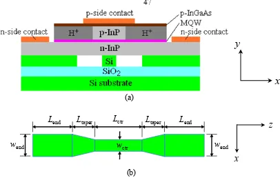
propagation direction in a 200-μm-long mode transformer with the optimal design. The equiripple behavior of both modes indicates that the total scattered power into the odd mode is minimized...41 4.1. Refractive index profile and optical mode profile of the InGaAsP epilayer ...44 4.2. (a) The InGaAsP epilayer bonded to a Si slab waveguide. (b) Confinement factor
for Si waveguide of the slab waveguide structure shown in (a). This is the maximal fraction of modal power in Si if the Si slab is replaced with a channel waveguide ...46 4.3. (a) Illustration of the cross-sectional view of the hybrid laser (not to scale). (b) Si
Lctr = 400 μm, wend = 1.2 μm, wctr = 0.6, 0.7, 0.8, or 0.9 μm. The tapers connecting the end and central sections have linear width variation...47 4.4. Quantum well confinement factor ΓQW as a function of the Si waveguide width w.
Inset: Calculated confinement factors of the III–V and the Si waveguide ...47 4.5. Fabrication flow chart of supermode hybrid Si/III–V lasers...51 4.6. SEM cross-sectional images of the InGaAsP epifilm on SOI by wafer bonding
after the InP substrate removal. (a) Zoom at one end of the epifilm. (b) Zoom at middle of the epifilm ...53 4.7. Annealing system for fabricating continuous-wave semiconductor lasers...55 4.8. (a) Optical microscope image of top view of a fabricated device. (b), (c) SEM
images of a cleaved end facet of a fabricated supermode Si/InGaAsP laser: (b) overview of the device, (c) close-up view at the center Si waveguide region. Approximate proton implanted regions are superimposed on the image for illustration ...56 5.1. Experimental setup for measuring (a) laser L–I curve, and (b) near-field emission
pattern and optical spectrum ...58 5.2. Threshold current density Jth and slope efficiency ηex as a function of the width of
5.3. Bonding interfacial layer confinement factor ΓBL as a function of the Si waveguide width w. The maximal confinement to the bonding interfacial layer is achieved at w = 0.73 μm ...60 5.4. (a) Optical spectrum of a typical device. (b) Evolution of the optical spectrum as
the pump current (voltage) increases. Higher pump level results in the expansion of the range of lasing modes to the longer wavelength side. Spectra in both (a) and (b) were measured with pulsed current injection...61 5.5. Near-field patterns of the edge emission from a device operated (a) below
threshold, (b) at threshold, and (c) above threshold. The modal confinement to the Si waveguide (especially when the mode is lasing) is obvious ... 63 5.6. Threshold voltage of evanescent Si/InGaAsP lasers with constant Si waveguide
widths. Measurements were taken in pulsed mode at 15 °C, with dc denoting
the duty cycle of the applied voltage ...63 5.7. (a) L–I–V curve of a 960-μm-long evanescent laser under CW operation at 15 °C.
(b) Lasing threshold current (in log scale) as a function of temperature (blue “+” signs) with a linear fit (red dashed line)...66 5.8. (a) Optical spectrum of a Si/InGaAsP evanescent laser (in dB scale).
7.1. Surface-emitting circular Bragg lasers: (a) circular DFB laser; (b) disk Bragg laser; (c) ring Bragg laser. Laser emission is coupled out of the resonator plane in the vertical direction via the Bragg gratings...73 8.1. Real part of the Green’s function G z z( , )′ with −∞ < z < ∞ and z′ between the
top and bottom surfaces of the laser resonator ...79 8.2. Radiation coupling coefficient h1 and feedback coupling coefficient h2 as a
function of the duty cycle dc of the Hankel-phased rectangular grating...81
9.1. Two types of boundary conditions for calculating reflectivities. (a) A(0) = B(0), r1(L) = A(L)/B(L); (b) B(L) = 0, r2(x0, L) = B(x0)/A(x0) ...85 10.1. Far-field intensity patterns of the fundamental mode of (a) circular DFB, (b) disk,
and (c) ring Bragg lasers ...94 10.2. Evolution of threshold gains of the 5 lowest-order modes of (a) circular DFB, (b)
disk, and (c) ring Bragg lasers...95 10.3. Unnormalized quality factor of circular DFB, disk, and ring Bragg lasers ...97 10.4. Modal area of circular DFB, disk, and ring Bragg lasers. The top surface area of
the laser resonator (π 2
b
x ) is also plotted as a reference ...98 10.5. Internal emission efficiency of circular DFB, disk, and ring Bragg lasers...99 11.1. Surface emission power Pem (in units of Psat) versus pump power level Ppump for
the fundamental mode of circular DFB laser (xb = 200) under uniform pumping.
11.2. Illustration of different pump profiles: (a) uniform; (b) Gaussian; (c) annular ...103 11.3. Device-size-dependent pump level Ppump and frequency detuning factor δ of the
List of Tables
4.1. InGaAsP epiwafer layer structure ...44 5.1. Test results of supermode (varying-width) lasers and evanescent (constant-width)
lasers ...59 8.1. Approximated layer structure for numerical study...79 10.1. Modal field patterns, along with their threshold gains (gA) and frequency
detuning factors (δ), of the circular DFB, disk, and ring Bragg lasers. All the three types of lasers have an exterior boundary radius of xb = 200 ...91
List of Publications
Invited Book Chapters
(1) Xiankai Sun and Amnon Yariv, “Surface-emitting circular Bragg lasers – a
promising next-generation on-chip light source for optical communications,” in Frontiers in Guided Wave Optics and Optoelectronics, Bishnu Pal (ed.), Intech, 2010. ISBN: 978-953-7619-82-4.
(2) Michael Shearn, Xiankai Sun, M. David Henry, Amnon Yariv, and Axel Scherer,
“Advanced plasma processing: etching, deposition, and wafer bonding techniques for semiconductor applications,” in Semiconductor Technologies, Jan Grym (ed.), Intech, 2010. ISBN: 978-953-307-080-3 (in press).
(3) Jacob Scheuer and Xiankai Sun, “Radial Bragg resonators,” in Photonic
Microresonator Research and Applications, Ioannis Chremmos, Otto Schwelb, and Nikolaos Uzunoglu (eds.), Springer, 2010. ISBN: 978-1-4419-1743-0 (in press).
Refereed Journal Papers
(1) Michael Shearn, Kenneth Diest, Xiankai Sun, Avi Zadok, Harry Atwater, Amnon
Yariv, and Axel Scherer, “Advanced silicon processing for active planar photonic devices,” Journal of Vacuum Science & Technology B, 27 (6): 3180–3182, Nov./Dec.
2009.
(2) Xiankai Sun and Amnon Yariv, “Surface-emitting circular DFB, disk-, and ring-
Bragg resonator lasers with chirped gratings. III: gain saturation effects and above-threshold analysis,” Optics Express, 17 (12): 10119–10125, Jun. 2009.
(3) Xiankai Sun, Avi Zadok, Michael J. Shearn, Kenneth A. Diest, Alireza Ghaffari,
Harry A. Atwater, Axel Scherer, and Amnon Yariv, “Electrically pumped hybrid evanescent Si/InGaAsP lasers,” Optics Letters, 34 (9): 1345–1347, May 2009.
(4) Xiankai Sun, Hsi-Chun Liu, and Amnon Yariv, “Adiabaticity criterion and the
shortest adiabatic mode transformer in a coupled-waveguide system,” Optics Letters,
(5) Xiankai Sun and Amnon Yariv, “Surface-emitting circular DFB, disk-, and ring-
Bragg resonator lasers with chirped gratings. II: nonuniform pumping and far-field patterns,” Optics Express, 17 (1): 1–6, Jan. 2009.
(6) Xiankai Sun and Amnon Yariv, “Surface-emitting circular DFB, disk-, and ring-
Bragg resonator lasers with chirped gratings: a unified theory and comparative study,” Optics Express, 16 (12): 9155–9164, Jun. 2008. (Selected for Virtual Journal of
Ultrafast Science, 7 (8), Aug. 2008)
(7) Xiankai Sun and Amnon Yariv, “Engineering supermode silicon/III–V hybrid
waveguides for laser oscillation,” Journal of the Optical Society of America B, 25 (6):
923–926, Jun. 2008.
(8) Lin Zhu, Xiankai Sun, Guy A. DeRose, Axel Scherer, and Amnon Yariv, “Room
temperature continuous wave operation of single-mode, edge-emitting photonic crystal Bragg lasers,” Optics Express, 16 (2): 502–506, Jan. 2008.
(9) Xiankai Sun and Amnon Yariv, “Modal properties and modal control in vertically
emitting annular Bragg lasers,” Optics Express, 15 (25): 17323–17333, Dec. 2007
(also in the Virtual Focus Issue on Physics and Applications of Microresonators). (10) Lin Zhu, Xiankai Sun, Guy A. DeRose, Axel Scherer, and Amnon Yariv, “Spatial
modal control of two dimensional photonic crystal Bragg lasers,” Optics Letters, 32
(16): 2273–2275, Aug. 2007.
(11) Amnon Yariv and Xiankai Sun, “Supermode Si/III-V hybrid lasers, optical amplifiers
and modulators: a proposal and analysis,” Optics Express, 15 (15): 9147–9151, Jul.
2007.
(12) Lin Zhu, Xiankai Sun, Guy A. DeRose, Axel Scherer, and Amnon Yariv,
“Continuous-wave operation of electrically-pumped, single-mode, edge-emitting photonic crystal lasers,” Applied Physics Letters, 90 (26): 261116, Jun. 2007.
(13) Xiankai Sun, Jacob Scheuer, and Amnon Yariv, “Optimal design and reduced
threshold in vertically emitting circular Bragg disk resonator lasers,” IEEE Journal of Selected Topics in Quantum Electronics, 13 (2): 359–366, Mar./Apr. 2007 (Special
Issue on Optical Micro- and Nanosystems).
Refereed Conference Papers
(1) Xiankai Sun, Michael J. Shearn, Avi Zadok, Marina S. Leite, Scott T. Steger, Harry
(2) Xiankai Sun and Amnon Yariv, “Above-threshold analysis of large-area, high-power,
vertically-emitting circular Bragg lasers,” Frontiers in Optics 2009, San Jose, CA, Oct. 2009.
(3) Xiankai Sun and Amnon Yariv, “A comparative study of modal properties of
surface-emitting circular Bragg micro-lasers,” CLEO/Pacific Rim 2009, Shanghai, China, Aug. 2009.
(4) Xiankai Sun and Amnon Yariv, “Supermode control in integrated hybrid Si/III–V
optoelectronic circuits for modal gain enhancement,” CLEO/Pacific Rim 2009, Shanghai, China, Aug. 2009.
(5) Xiankai Sun, Hsi-Chun Liu, and Amnon Yariv, “How short can an adiabatic mode
transformer be in a coupled waveguide system?” CLEO/IQEC 2009, Baltimore, MD, May 2009.
(6) Michael Shearn, Kenneth Diest, Xiankai Sun, Avi Zadok, Amnon Yariv, Axel
Scherer, “Advanced silicon processing for active integrated photonic devices,” EIPBN 2009, Marco Island, FL, May 2009.
(7) Xiankai Sun, Avi Zadok, Michael J. Shearn, Kenneth A. Diest, Alireza Ghaffari,
Harry A. Atwater, Axel Scherer, and Amnon Yariv, “Hybrid electrically pumped evanescent Si/InGaAsP lasers,” OFC/NFOEC 2009, San Diego, CA, Mar. 2009.
(8) Xiankai Sun and Amnon Yariv, “A unified theory for surface emitting chirped
circular grating lasers,” SPIE Photonics West 2009, San Jose, CA, Jan. 2009.
(9) Xiankai Sun and Amnon Yariv, “Engineering surface-emitting annular Bragg lasers
for single-mode, high-efficiency, high-power applications,” LEOS Annual Meeting 2008, Newport Beach, CA, Nov. 2008.
(10) Xiankai Sun and Amnon Yariv, “Designing large-area, high-efficiency,
single-defect-mode vertically-emitting annular Bragg lasers,” Frontiers in Optics 2008, Rochester, NY, Oct. 2008.
(11) Lin Zhu, Xiankai Sun, Guy DeRose, Axel Scherer, and Amnon Yariv, “Room
temperature continuous wave operation of single-mode, edge-emitting photonic crystal Bragg lasers,” CLEO/QELS 2008, San Jose, CA, May 2008.
(12) Xiankai Sun, Jacob Scheuer, and Amnon Yariv, “Optimal design of vertically
Patents
(1) Amnon Yariv and Xiankai Sun, “Hybrid Waveguide Systems and Related Methods,”
Glossary of Acronyms
AlGaInAs: aluminum gallium indium arsenide
BC: boundary condition BCB: benzocyclobutene
CMOS: complementary metal–oxide–semiconductor CW: continuous wave
DBR: distributed Bragg reflector DFB: distributed feedback
e-beam: electron beam
GaAs: gallium arsenide GaP: gallium phosphide
InGaAsP: indium gallium arsenide phosphide
InP: indium phosphide IR: infrared
MQW: multiple quantum well QW: quantum well
RC: resistive–capacitive
Part I
Chapter 1
Introduction
1.1 Motivation of a Laser on Silicon
The voracious appetite for a higher rate of data processing and transmission of computers and networks has resulted in an ever-increasing density of the silicon (Si) large-scale integration. However, this technology is approaching a bottleneck because of the inherent problems associated with the copper interconnections.
The electronic integration with higher device density consumes more power and at the same time generates more heat in a unit area on the chip. It is difficult to find an effective way to dissipate the generated heat. Figure 1.1 is a graph from Professor Bahram Jalali’s paper in Nature Photonics [1]. It demonstrates clearly the exponential growth of the heat density on the computer chips. The heat dissipation density is exceeding that of a hot plate, and in fact it is not far away from that of a nuclear reactor. The heat dissipation issue itself sets a limitation on the future growth of the integration density.
(RC) delay. When the data rates approach 10 Gb s−1 and beyond, optical communication becomes a superior and perhaps even the only solution on the horizon simply because of its considerably larger operational bandwidth. This is the underlying driving force of the research of Si photonics.
[image:28.612.112.528.67.349.2]In a photonic circuit, one should have various functional devices for light generation, guiding, modulation, amplification, filtering, and detection. Indeed, an on-chip integrable laser is an indispensable element in active photonic circuits. Unfortunately, Si is a poor converter of electricity to light, due to its indirect semiconductor bandgap. In addition, the epitaxial growth of standard GaAs- and InP-based direct bandgap materials on Si substrates has proven to be a major obstacle, due to the mismatch in lattice constants and in thermal Fig. 1.1. Exponential growth of the heat density on the computer chips. The power density on a silicon chip has already exceeded 100 W cm−2. Reprinted with permission from [1],
expansion coefficients [2]. Despite these difficulties, recent years witnessed a reawakening of the interest in Si-integrated lasers, with various approaches toward its practical realization.
1.2 Review of Various Integration Schemes
Numerous avenues have been followed toward obtaining Si-integrated lasers, including Raman amplification [3], rare-earth doping [4], and nanocrystalline Si structures [5]. Since III–V semiconductor compounds have been well known as efficient light emitting materials, integration of these materials on Si platform is considered as the most promising approach, although band-engineered epitaxial germanium (Ge) has recently been shown to be a potential laser material. In the following we will review several schemes that are being implemented to integrate the active materials on Si.
Direct Growth of Active Materials on Si
injected lasers grown by metal organic vapor phase epitaxy have been demonstrated for GaP-based broad-area Ga(NAsP)/GaP single-quantum-well heterostructures near room temperature [7]. The work on growing the dilute nitride Ga(NAsP) on Si substrate using GaP as the buffer layer to achieve lasing for practical uses is still underway [8].
In the meantime, the study of using Ge as the active material on Si substrate has made good progress [9-11]. Due to its pseudodirect gap properties and compatibility with Si complementary metal–oxide–semiconductor (CMOS) technology, Ge may also be used in the electronic–photonic integration. It has been shown that Ge can be band engineered by tensile strain and n-type doping to achieve efficient light emission and optical gain from its direct gap transition. Indeed, the optical gain in the wavelength range of 1600– 1608 nm from n+ tensile-strained epitaxial Ge on Si (100) substrate has been observed [9]. Optical pumped lasing action at room temperature edge-emitted from such Ge waveguides has recently been achieved [11]. The laser threshold is still very high, and further investigation on p-type doping in Ge is necessary to achieve an electrically pumped device. Figure 1.2 shows the emission spectra, cross-sectional scanning electron microscope (SEM) image of the Ge waveguide and a schematic drawing of the experimental setup for optical pumping.
Recess Integration of Lasers with Waveguides on Si
Fig. 1.2. Edge-emission spectra of a Ge waveguide with mirror polished facets under 1064 nm excitation from a Q-switched laser with a pulse duration of 1.5 ns and a repetition rate of 1 kHz. The three spectra at 1.5, 6.0, and 50 μJ/pulse pumping power correspond to spontaneous emission, threshold for lasing, and laser emission. The inset shows a cross-sectional SEM picture of the Ge waveguide and a schematic drawing of the experimental setup for optical pumping. Reprinted with permission from [11],
© 2010 OSA.
(a) (b)
[image:31.612.181.449.71.313.2]claimed to be highly modular and consistent with standard Si-CMOS front- and back-end processing.
The process starts with fabricating silicon oxy-nitride waveguides in silicon oxide and then etching recesses for the laser platelets. The ridge waveguide lasers, prefabricated from typical III–V materials, were cleaved by a novel microcleaving technique to produce 6 μm thick, 100 μm wide, 300 μm long platelets with good end facets. These laser platelets were manually picked and bonded into the recesses, after which the top contact was fabricated. The light emitted from the laser is coaxially coupled to the silicon oxy-nitride waveguide for chip transport. As expected, the biggest obstacle of this scheme is the high coupling loss arising from the misalignment between the laser and the waveguide.
Figure 1.3(a) is a schematic drawing of the recess integration. Figure 1.3(b) is a SEM image of a microcleaved III–V ridge waveguide platelet positioned in a dielectric recess on Si substrate and aligned with a silicon oxy-nitride waveguide.
Integrating III–V Materials with Si by Wafer Bonding
successful examples of using these two types of wafer bonding techniques are shown below.
In [13, 14], an InP/InGaAsP thin film epitaxial layer was bonded to a silicon-on-insulator (SOI) waveguide circuit by adhesive bonding using divinyl-tetramethyldisiloxane-benzocyclobutene (DVS-BCB). Lasers and photodetectors were fabricated in the bonded InP/InGaAsP epitaxial layer. Light emitted from the laser is vertically coupled into the Si waveguide with an inverted taper approach. Figure 1.4(a)
shows an electrically injected InGaAsP microdisk laser coupled with an underlying submicron Si wire waveguide. The microdisk laser has a diameter of 7.5 μm and a thickness of 1 μm. The laser with emission wavelength at 1.6 μm has a low threshold current of 0.5 mA under continuous-wave operation at room temperature, and a SOI-coupled maximum unidirectional output power of 10 μW. Figure 1.4(b) is a SEM image
(a) (b)
Fig. 1.4. Schematic of the heterogeneous microdisk laser structure, showing the disk cavity, SOI wire waveguide, bottom contact layer, tunnel junction, and metal contacts. (b) Cross section of the bonded structure, zooming in at the interface showing benzocyclobutene (BCB) as the bonding layer. Reprinted with permission from [13, 14],
showing the cross section of the wafer-bonded structure with DVS-BCB as the bonding interlayer.
In applications that require direct contact of the two materials, i.e., with no intermediate bonding layers, the above adhesive bonding is inapplicable when direct coupling is required through bonding. The direct wafer bonding is a process in which the adhesion between two semiconductor surfaces occurs as a result of chemical bonds established between the atoms and molecules from the two surfaces. The adhesion is weak at room temperature (because of the Van der Waals forces) and this can be greatly enhanced with a high-temperature thermal annealing to transform the weak bonds into stronger covalent bonds. However, this high-temperature annealing step induces material degradation and is incompatible with back-end Si CMOS processing. For this purpose, many efforts have been put into reducing the annealing temperature while keeping a strong bonding [15-17]. A special surface preparation process (surface activation) is usually performed to change and control the bonding mechanism by controlling the surface chemistry. Surface activation can be performed by a dip of the substrates in chemical solutions (wet activation) [18] or by a plasma treatment of the surface (dry activation) [19].
of the formation of interfacial bubbles and voids during postbonding annealing. Additionally, the plasma treatment generates a very smooth and reactive thin oxide layer that helps in bonding process. As a powerful tool of heterogeneous photonic integration, this low-temperature O2 plasma-assisted wafer bonding technique has given birth to a series of hybrid Si/III–V photonic devices, among which the Si evanescent laser will be introduced in the next section as a representative.
1.3 Introduction of Si/III–V Evanescent Lasers
Using the direct wafer bonding technique, an active AlGaInAs material is transferred onto a prepatterned Si-on-insulator wafer. The top AlGaInAs layers, which include multiple quantum wells (MQWs), are then patterned postbonding to produce Fabry–Pérot [20], racetrack [21] and distributed-feedback (DFB) lasers [22]. The bonded structure is designed to support a joint optical mode, whose profile overlaps both materials. During operation, this optical mode is guided in a Si waveguide and is amplified by its evanescent penetration into a III–V slab waveguide, which provides optical gain when electric current is injected [see Fig. 1.5(a) and (b)], and thus these devices are referred to as Si/AlGaInAs evanescent lasers [20].
lasers had to be fabricated very long, whose large footprint reduces the density of photonic integration on a chip. This is the major hurdle to be overcome before this hybrid Si/III–V technology can be industrialized.
y
x
(a)
(b)
(c) (d)
[image:37.612.115.534.72.564.2]Chapter 2
Supermode Theory
The term “supermode” was initially introduced by Kapon et al. to analyze the modes propagating in semiconductor laser arrays [23]. The formalism was used formally in the textbook Optical Electronics in Modern Communications [24]. Here the “supermodes” refer to the eigenmodes of a system of two (or even more) coupled optical waveguides. In this chapter we will first derive the supermodes of a coupled optical waveguide system, then show the numerical simulation results based on a hybrid waveguide structure to support the theory.
This chapter is reproduced and adapted with permission from [25-27], © 2007, 2008 OSA, © 2009 IEEE.
2.1 Derivation of Supermodes of Coupled Optical Waveguides
We start with the Maxwell’s equations,
(
)
(
)
( )
0 0
,
.
H E P
t
E H M H
t t
ε
μ μ
∂
⎧∇× = +
⎪⎪ ∂
⎨ ∂ ∂
⎪∇× = − + = −
⎪ ∂ ∂
⎩
(2.1)
(
)
(
)
(
)
(
)
(
)
2 0 2
2 2
0 0
2 pert 2 pert .
E H E P
t t
E P P E P
t t
μ μ ε
μ ε μ ε
∂ ∂
∇× ∇× = − ∇× = − +
∂ ∂
∂ ∂
= − + + = − +
∂ ∂
(2.2)
Using vector identity and ∇ ⋅ =E 0,
(
E) (
E)
2E 2E∇× ∇× = ∇ ∇ ⋅ − ∇ = −∇ , (2.3)
we have
2 2
2
2 2
pert P E
E
t t
με ∂ μ ∂
∇ − =
∂ ∂ . (2.4)
Without loss of generality, we consider the case of two uncoupled 1-D (slab) waveguides with refractive index distributions ( )n xa and n xb( ) (see Fig. 2.1). The normalized transverse eigenmodes of each waveguide are ( )a ( )
y x
ξ and ( )b ( ) y x
[image:39.612.144.502.70.297.2]ξ , and their Fig. 2.1. Refractive index profile for the uncoupled waveguides na(x) and nb(x) and for the
propagation constants are βa and βb. The modal field of the coupled guide structure with an index distribution ( )n xc can be expressed as a superposition of the uncoupled fields,
( ) ( ) ( ) ( )
( , ) ( ) a ( ) i t az ( ) b ( ) i t bz
y y y
E x z =A z ξ x e ω β− +B z ξ x e ω β− , (2.5)
where ( )a ( ) y x
ξ and ( )b ( ) y x
ξ satisfy
2
2 ( ) 2 2 ( ) 0
2 2
2 ( ) 2 2 ( ) 0
2
( ) ( ) ( ) 0,
( ) ( ) ( ) 0.
a a
a y a y
b b
b y b y
x n x x
x
x n x x
x
β ξ ω με ξ
β ξ ω με ξ
⎛ ∂ − ⎞ + = ⎜∂ ⎟ ⎝ ⎠ ⎛ ∂ − ⎞ + = ⎜∂ ⎟ ⎝ ⎠ (2.6)
Substitution of (2.5) into (2.4) yields
2 ( ) ( )
2
2 i az i zb pert
i t a b
a y b y
P
A B
e i e e
z z t
β β
ω ⎡− ⎛β ∂ ξ − +β ∂ ξ − ⎞⎤=μ∂
⎜ ⎟
⎢ ⎝ ∂ ∂ ⎠⎥ ∂
⎣ ⎦ , (2.7)
where we have used (2.6) and the “slow-varying” approximations 2A2 a A
z β z
∂ ∂
∂ ∂ and
2
2 b
B B
z β z
∂ ∂
∂ ∂ . The perturbation polarization is
0 0 0
( ) ( ) 2 ( ) ( )
0
( ) ( )
2 ( ) 2 ( )
0 0 ( ) 0 ( , ) ( , ) ( , ) ( , ) ( , ) ( ) ( ) ( ) ( ) ( ) ( ) ( ) ( ) ( ) ( ) ( ) ( ) ( ) a b a b coup orig
pert r r
i t z i t z
a b
c y y
i t z i t z
a b
a y b y
i t a
y
P r t P r t P r t E r t E r t
n x A z x e B z x e
n x A z x e n x B z x e
e A z x n
ω β ω β
ω β ω β
ω
ε ε ε ε
ε ξ ξ
ε ξ ε ξ
ε ξ − − − − = − = − ⎡ ⎤ = ⎣ + ⎦ − −
=
(
2( ) 2( ))
i az ( ) ( )b ( )(
2( ) 2( ))
i zb .c x n x ea β B z ξy x n xc n x eb β
− −
⎡ − + − ⎤
⎣ ⎦
(2.8)
Plugging (2.8) into (2.7), multiplying both sides by ( )a ( ) y x
(
) (
)
(
)
2 2
( ) 2 2 0 2
( ) ( ) 2 2
4 ( ) ( ) ( ) ( )
( ) ( ) ( ) ( ) ( ) ,
a a
b
i z a i z
y c a
i z
a b
y y c b
dA
i e x n x n x dxA z e
dz t
x x n x n x dxB z e
β β
β
ω ε ξ
ξ ξ ∞ − − −∞ ∞ − −∞ ∂ ⎡ − = ⎢⎣ − ∂ ⎤ + − ⎥⎦
∫
∫
(2.9)where we have used the mode orthogonality condition,
( ) ( )
,
2 ( ) ( )
a b
y y a b
a
x x dx ωμ
ξ ξ δ
β
∞
−∞ =
∫
. (2.10)Likewise,
(
)
(
) (
)
2
( ) ( ) 2 2 0 2
2
( ) 2 2
4 ( ) ( ) ( ) ( ) ( )
( ) ( ) ( ) ( ) .
b a
b
i z a b i z
y y c a
i z b
y c b
dB
i e x x n x n x dxA z e
dz t
x n x n x dxB z e
β β
β
ω ε ξ ξ
ξ ∞ − − −∞ ∞ − −∞ ∂ ⎡ − = ⎢⎣ − ∂ ⎤ + − ⎥⎦
∫
∫
(2.11)If we introduce the definitions,
(
)
2 2 ( ) ( ) 0, ,
2 2 2 ( , ) 0 , , ( ) ( ) ( ) ( ) , 4 ( ) ( ) ( ) , 4 a b
ab ba c b a
a b
a b c a b
n x n x x x dx
M n x n x x dx
ωε
κ ξ ξ
ωε ξ ∞ −∞ ∞ −∞ ⎡ ⎤ = ⎣ − ⎦ ⎡ ⎤ = ⎣ − ⎦
∫
∫
(2.12)then we have
( ) ( ) , . b a a b i z ab a i z ba b dA
i Be iM A
dz dB
i Ae iM B
dz β β β β κ κ − − − − ⎧ = − − ⎪⎪ ⎨ ⎪ = − − ⎪⎩ (2.13)
To simplify (2.13), we introduce A Ae= −iM za and B Be= −iM zb and define
, , ,
a b a b Ma b
β′ =β + ,
then we get
(
( ) ( ))
( , ) i t i az a i zb by y y
E x z =eω Ae−β′ξ +Be−β′ξ , (2.14)
( ) ( ) , . b a b a i z ab i z ba dA i Be dz dB i Ae dz β β β β κ κ ′ ′ − − ′− ′ ⎧ = − ⎪⎪ ⎨ ⎪ = − ⎪⎩ (2.15)
Eq. (2.14) can be expressed in the basis of
{
( )a , ( )b}
y yξ ξ as a column vector,
(1) (2) b a i z i z Be E E E Ae β β ′ − ′ −
= = , (2.16)
so that
(1) (2)
b ba
ab a
i i E
dE CE i i dz E β κ κ β ′ − − = = ′
− − . (2.17)
A propagating supermode, by its definition, is a field solution whose z (the propagation direction) dependence is only through a propagation phase factor ei zγ , i.e.,
( ) (0) i z E z =E eγ , so
dE i E
dz = γ . (2.18)
Combining (2.17) and (2.18) yields
(
C i I E− γ)
=0, (2.19)i.e.,
(1) (2) 0
b ba
ab a
i i i E
i i i E
β γ κ
κ β γ
′
− − −
= ′
− − − . (2.20)
To have nontrivial solutions, we require that
(
)
22 0
b ba
b a a b
ab a
i i i
i i i
β γ κ
β β γ γ β β κ
κ β γ
′
− − −
′ ′ ′ ′
= − − − + + =
′
where
(
)
12 ab baκ ≡ κ κ , leading to
(
)
2 21 4 2 2 a b b a β β
γ = − ′+ ′ ± β′−β′ + κ . (2.22)
Let
2 a b
β β
β = ′+ ′ ,
2 b a
β β
δ = ′− ′ , and S = δ2+κ 2 , then
1,2 S
γ = − ±β , and the
corresponding eigenfields (supermodes) are
( ) ( ) 1 2 (1) 1 1 (2) 1 1 (1) 2 2 (2) 2 2 , 1 . 1 ba
i S z ba i z
b
ba
i S z ba i z
b
E i
E e S e
i i
E
E i
E e S e
i i E β γ β γ κ κ δ β γ κ κ δ β γ − − − + − = = ′ = + − − − = = ′ = − − − (2.23)
There are three limiting cases of our special interest: (1) δ <0, δ κ ,
so 1 2 2 2 2 1 1 1 2 2
S δ κ δ κ δ κ
δ δ δ
⎛ ⎞ ⎛ ⎞
= ⎜⎜ + ⎟⎟ ≈ ⎜⎜ + ⎟⎟= − −
⎝ ⎠ ⎝ ⎠ , and
1 1 2 2 2 1 , 1 1 . 2 1 1 b b a a
i z i z
ab
ba
i z i z
E e e
E e e
β β β β δ κ ε κ ε δ ′ ′ − − ′ ′ − − − = = − = = (2.24)
where 1 , 2
2 2
ab ba
κ κ
ε ε
δ δ
≡ ≡ and 0<ε ε1, 2 1. (2) δ =0,
( ) ( ) 1 2 , 1 1 . 1 1 o e ba
i z i z
ba
i z i z
E e e
E e e
β κ β
β κ β
κ η κ κ η κ − − − − + − − − = = = = (2.25) where 1 2 1 ba ab κ η κ ⎛ ⎞ ≡⎜ ⎟ ≈ ⎝ ⎠ .
(3) δ >0,δ κ ,
so 1 2 2 2 2 1 2
S δ κ δ κ
δ δ ⎛ ⎞ ⎜ ⎟ = + ≈ + ⎜ ⎟ ⎝ ⎠ , and 2 1 1 2 , 2 1 1 2 1 . 1 1 a a b b ba
i z i z
i z i z
ab
E e e
E e e
β β β β κ ε δ δ κ ε ′ ′ − − ′ ′ − − − − = = = = (2.26) Fig. 2.2. Field profile of the two supermodes Eo and Ee in the three limiting cases: δ< 0,
The field profiles of the supermodes in the three cases are illustrated in Fig. 2.2, where the subscripts “o” (odd) and “e” (even) refer to the modal symmetry.
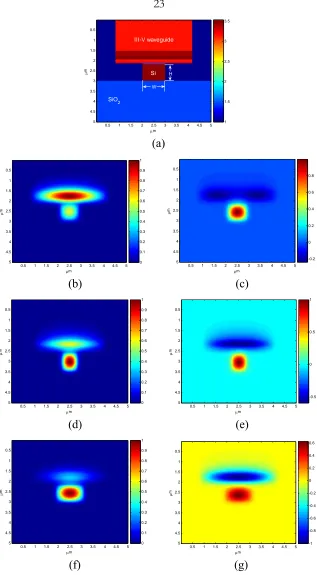
2.2 Numerical Verification of the Supermode Theory
To numerically verify the supermode theory, the III–V wafer structure employed in the work of Fang et al. (see the detailed epiwafer structure in Table 1 of [20]) is used here as an example. The thickness of the separate confinement heterostructure (SCH) layer and the n -layer are modified to be 80 and 200 nm, respectively, to increase the modal confinement to the quantum wells. Additionally, we will design the Si waveguide to be a ridge rather than a rib waveguide to facilitate the coupling between the III–V and Si.
The supermodes of the hybrid waveguides arise from the coupling between all the original modes of the III–V waveguide and the Si waveguide. However, we are interested in the two lowest-order supermodes, which result from the coupling between the fundamental modes of the III–V and the Si waveguides. In the simulation, the III–V waveguide has a width of 3.30 μm. The effective index neff is 3.2588 at the wavelength
1.55 μm as calculated with a mode solver. Figure 2.3(a) and (b) show the index profile and the fundamental mode of the III–V waveguide. For Si waveguide, we use a typical SOI ridge waveguide with a fixed height H and a longitudinally varying width W. Figure 2.3(c)
profiles of the even and odd supermodes of the hybrid waveguides in the three representative cases. The phase-matching condition (δ→0) is satisfied in Fig. 2.4(d) and (e)
where the Si waveguide has a height H = 0.84 μm and a width W = 0.65 μm with neff of
3.2529. In this case, for both even and odd supermodes, the modal power is roughly evenly divided between the III–V and the Si waveguides, as predicted by the supermode theory.
Now we understand that the even and odd supermodes coexist in the coupled-waveguide system, though propagating at different phase velocities. In practice, we want a single mode to be in operation in such a system. We can separate the two supermodes by adiabatically tapering the Si waveguide width to provide different amount of feedback to different modes. Only the mode having stronger feedback will lase. Figure 2.5(a) shows the confinement factors in the active region (including quantum wells and barriers in between)
Γact, and in the Si waveguide ΓSi, for the lowest-order even supermode, as a function of the Si waveguide width W. Figure 2.5(b) plots the confinement factors in the whole III–V waveguide ΓIII–V and in the Si waveguide ΓSi, and the mismatch parameter δ as a function of Si waveguide width W. As expected, these three curves intersect at one point where the phase is matched (δ→0) and the modal power is also evenly distributed in each waveguide. Figure 2.5(c) displays the absolute value of the mismatch parameter |δ| and the coupling
μm
μ
m
0.5 1 1.5 2 2.5 3 3.5 4 4.5 5 0.5 1 1.5 2 2.5 3 3.5 4 4.5 5 1 1.5 2 2.5 3 3.5 III-V waveguide μm μ m
0.5 1 1.5 2 2.5 3 3.5 4 4.5 5 0.5 1 1.5 2 2.5 3 3.5 4 4.5 5 0 0.1 0.2 0.3 0.4 0.5 0.6 0.7 0.8 0.9 1
(a) (b)
μm
μ
m
0.5 1 1.5 2 2.5 3 3.5 4 4.5 5 0.5 1 1.5 2 2.5 3 3.5 4 4.5 5 1 1.5 2 2.5 3 Si W H μm μ m
0.5 1 1.5 2 2.5 3 3.5 4 4.5 5 0.5 1 1.5 2 2.5 3 3.5 4 4.5 5 0 0.1 0.2 0.3 0.4 0.5 0.6 0.7 0.8 0.9 1
(c) (d)
[image:47.612.164.483.75.370.2]μm
μ
m
0.5 1 1.5 2 2.5 3 3.5 4 4.5 5 0.5 1 1.5 2 2.5 3 3.5 4 4.5 5 1 1.5 2 2.5 3 3.5 III-V waveguide Si SiO 2 W H (a) μm μ m
0.5 1 1.5 2 2.5 3 3.5 4 4.5 5 0.5 1 1.5 2 2.5 3 3.5 4 4.5 5 0 0.1 0.2 0.3 0.4 0.5 0.6 0.7 0.8 0.9 1 μm μ m
0.5 1 1.5 2 2.5 3 3.5 4 4.5 5 0.5 1 1.5 2 2.5 3 3.5 4 4.5 5 -0.2 0 0.2 0.4 0.6 0.8
(b) (c)
μm
μ
m
0.5 1 1.5 2 2.5 3 3.5 4 4.5 5 0.5 1 1.5 2 2.5 3 3.5 4 4.5 5 0 0.1 0.2 0.3 0.4 0.5 0.6 0.7 0.8 0.9 1 μm μ m
0.5 1 1.5 2 2.5 3 3.5 4 4.5 5 0.5 1 1.5 2 2.5 3 3.5 4 4.5 5 -0.5 0 0.5 1
(d) (e)
μm
μ
m
0.5 1 1.5 2 2.5 3 3.5 4 4.5 5 0.5 1 1.5 2 2.5 3 3.5 4 4.5 5 0 0.1 0.2 0.3 0.4 0.5 0.6 0.7 0.8 0.9 1 μm μ m
0.5 1 1.5 2 2.5 3 3.5 4 4.5 5 0.5 1 1.5 2 2.5 3 3.5 4 4.5 5 -1 -0.8 -0.6 -0.4 -0.2 0 0.2 0.4 0.6
(f) (g)
[image:48.612.165.482.75.650.2]0.4 0.45 0.5 0.55 0.6 0.65 0.7 0.75 0.8 0.85 0.9 0 0.04 0.08 0.12 0.16 0.2 0.24 0.28 0.32 0.36 0.4
Si waveguide width W (μm)
A c ti v e re gi on c o n fin em e n t fac to r Γac t
0.4 0.45 0.5 0.55 0.6 0.65 0.7 0.75 0.8 0.85 0.90
0.1 0.2 0.3 0.4 0.5 0.6 0.7 0.8 0.9 1 Si c o n fi n em ent f a c tor Γ Si (a)
0.4 0.45 0.5 0.55 0.6 0.65 0.7 0.75 0.8 0.85 0.9
0 0.1 0.2 0.3 0.4 0.5 0.6 0.7 0.8 0.9 1
Si waveguide width W (μm)
Conf in e m e n t f a ct or Γ
0.4 0.45 0.5 0.55 0.6 0.65 0.7 0.75 0.8 0.85 0.9-350
-280 -210 -140 -70 0 70 140 210 280 350 M is m a tch par am e ter δ (m m -1 )
In III-V waveguide In Si waveguide
(b)
0.4 0.45 0.5 0.55 0.6 0.65 0.7 0.75 0.8 0.85 0.9
0 50 100 150 200 250 300 350 |δ | ( m m -1)
Si waveguide width W (μm)
0.4 0.45 0.5 0.55 0.6 0.65 0.7 0.75 0.8 0.85 0.90
50 100 150 200 250 300 350 κ (m m -1) (c)
Fig. 2.5. (a) Confinement factors in the active region (Γact) and in the Si waveguide (ΓSi) as a function of the Si waveguide width W. (b) Confinement factors in the III–V (ΓIII–V) and Si waveguide (ΓSi), and the mismatch parameter δ as a function of the Si waveguide width
2.3 Proposal of Supermode Si/III–V Lasers and Beyond
As shown in Figs. 2.4 and 2.5, with a proper choice of the Si waveguide width, we can direct the modal power to the amplifying III–V waveguide or to the Si waveguide, thereby avoiding the degraded performance that results from the reliance on the evanescent field. At the in/out coupling regions, the modal power is diverted to the Si waveguide by adiabatically increasing its width. This makes for efficient coupling to the
(a)
[image:50.612.145.503.284.656.2](b)
outside Si photonic circuit.
As marked with the red line in Fig. 2.6(a), the mode starts propagating from left to right in the upper left III–V waveguide where it is amplified. It then enters the adiabatic transformer section where the width of the Si waveguide increases so as to cause δ to change from δ < 0 to δ > 0. This causes the modal power to shift to the lower low-loss Si waveguide where it is partially reflected from the right output facet. The reflected field retraces its path till reflected from the upper left facet thus completing the round trip. The other mode is suppressed due to the high distributed loss along the path and the absence of feedback mechanism. A considerable enhancement of modal gain is the most direct advantage of the supermode control. Based on the calculated modal confinement factors in the active region Γact and in the Si waveguide ΓSi for different Si waveguide widths [Fig.
2.5(a)], the modal gain can be increased up to five times, if the adiabatic tapers are efficient in mode transformation and designed as short as possible [26].
The main advantage of this “spatial switching” of the modal power is to obtain maximum achievable gain from the inverted medium since the peak modal field and not just an evanescent tail induce the amplifying transitions in the gain (III–V) region. Bearing in mind the idea of supermode control, we can make another laser configuration [Fig.
2.6(b)] that is more symmetric in the longitudinal extension. The laser light emits from both left and right Si end facets, and two adiabatic tapers are used to transform the supermode between Si and III–V.
[Fig. 2.7(a)], light is first coupled into the Si waveguide (δ > 0), then switched to the upper III–V section (δ < 0) for amplification or modulation, finally coupled back to Si waveguide (δ > 0) for output coupling. This principle can also be applied to make a photodetector [Fig.
2.7(b)]: as the light is spatially switched from the Si waveguide to the upper III–V waveguide, which under reversed bias is highly absorbing, extra electron–hole pairs will be
(a)
(b)
[image:52.612.170.478.73.459.2]excited across the p–n junction contributing to the conductivity, which reflects in the change of current in the outside electric circuit.
Fig. 2.8. Conception of
future
large-scale, high-e
fficiency hybrid optoele
ctroni
c circ
uitry. Device
s wit
h differe
nt optical fun
ctions
can be integr
ated on
the Si platform. T
he light tra
nsportation f
rom one module to anot
he
r can be
on-chip by Si wave
guides
or
Chapter 3
Adiabaticity Theorem and the
Shortest Adiabatic Taper Design
In Chapter 2 we have shown that as the refractive index profile n(x, y) of the coupled-waveguide system varies along the longitudinal direction (z), the corresponding local normal modes (supermodes) Ee(x, y) and Eo(x, y) will change accordingly. For such
longitudinally variant waveguide structure, these supermodes are actually z dependent, and each cross section of the waveguide system has its own set of supermodes. In analogy to the famous adiabaticity theorem in quantum mechanics, if the change in n(x, y), which can be the variation in waveguide geometry and/or refractive index, is slow enough along the propagation direction (z), we are able to approximate the solutions of the Maxwell equations in the real configuration by means of “stationary” supermodes of the local waveguide structure. In such a case, a particular supermode at a z plane will go over continuously into the corresponding supermode at any other z plane.
possible while keeping the scattering to other unwanted modes as low as possible. In this chapter we derive a universal criterion for designing such adiabatic mode transformers based on a perturbation approach. The criterion relates ε, the fraction of power scattered into the unwanted mode, to waveguide design parameters and gives the shortest possible length of an adiabatic mode transformer that is approximately 2/πε1/2 times the distance of maximal power transfer between the waveguides. After that the numerical results obtained based on a transfer-matrix formalism are presented to support this theoretical derivation.
This chapter is reproduced and adapted with permission from [28], © 2009 OSA.
3.1 Derivation of the Adiabaticity Criterion
The optimal design procedure of adiabatic mode transformers has been proposed in different ways. Love et al. first studied the fiber tapers, suggesting that for a given taper length the optimal delineating curve should have the local taper angle inversely proportional to the local beat length [30, 43]. This design principle was also employed in [42] and [44] in experiments. Another design concept is based on equalization of the single step loss (defined as the overlap integral of the modes in two adjacent segments) along the taper [45, 46]. Since those analyses depended on the stationary field distributions and did not include the wave propagation behavior, they did not point out the optimal taper length with which a certain coupling efficiency could be achieved. Taking into account the supermode propagating behavior, we will derive a universal criterion for the adiabatic mode transition in a coupled-waveguide system and suggest the shortest possible length of an adiabatic mode transformer for any given power transfer efficiency.
The mode transformer to be analyzed here is based on a coupled-waveguide system shown in Fig. 3.1. It consists of two waveguides, namely waveguide 1 and waveguide 2,
placed in close proximity to each other. The refractive index or geometry of at least one waveguide is gradually varied along the propagation direction z. Light is coupled into this transformer at input plane z = zi (= 0) and out at output plane z = zf. As discussed in Chapter
1 2 1 2 1 1 ( ) 2 1 e e
i z i z S
z e e
S β β δ δ − − ⎛ − ⎞ ⎜ ⎟ ⎝ ⎠ = = ⎛ + ⎞ ⎜ ⎟ ⎝ ⎠ e e
e e and
1 2 1 2 1 1 ( ) 2 1 o o
i z i z S
z e e
S β β δ δ − − ⎛ ⎞ − +⎜ ⎟ ⎝ ⎠ = = ⎛ − ⎞ ⎜ ⎟ ⎝ ⎠ o o
e e , (3.1)
where δ = (β2 − β1)/2 is the mismatch of propagation constants between the individual uncoupled waveguide modes, 2S = 2(δ2 + κ2)1/2 = βe − βo is the difference of propagation
constants of the supermodes, and κ is the coupling strength between waveguides 1 and 2.
Figure 3.2 plots the corresponding dispersion curve of the propagation constants along z. Note that the modal profiles (3.1) of the supermodes are z dependent through the parameters δ and S. For both supermodes ee and eo, when δ < 0 and |δ| κ, the mode substantially resides in one waveguide, and when δ > 0 and δ κ, the mode is Fig. 3.1. Model of the adiabatic mode transformer based on two coupled waveguides 1and 2, placed in close proximity to each other. The geometry of waveguide 2 is gradually
varied along the z direction. Light is coupled in at plane z = zi (= 0) and out at plane z = zf.
substantially in the other waveguide. At the phase-matching point z0 where δ = 0 the optical power is evenly distributed in the two waveguides [25]. Our task is to design this coupled-waveguide system such that a supermode can transform adiabatically in the shortest distance with the parameter δ sweeping from a negative value to a positive value, while keeping the coupling to the other supermode below a certain level.
The total field in the mode transformer can be expressed as a linear combination of the supermodes with their phases accumulated,
β
eβ
oz
β
1β
2z
=
z
i= 0
β
2
S
z
=
z
fz
=
z
0Fig. 3.2. Dispersion curves of the propagation constants along z. β1 and β2 correspond to the propagation constants of the individual uncoupled waveguide modes. They cross at the phase-matching point z0. βe and βo are the propagation constants of the even and odd
supermodes of the coupled-waveguide system. 2S = βe− βo denotes the difference between
0 ,
( ) j( ) exp z j( ) j e o
z a z i β z dz
=
⎡ ′ ′⎤
= ⎢− ⎥
⎣ ⎦
∑
j∫
E e . (3.2)
Considering a guided optical wave paraxially propagating along the +z direction in a slowly varying waveguide, the total field satisfies the Fresnel equation [48],
ˆ ( ) ( ) z
i∂ E z =B zE , (3.3)
where ˆB is the Fresnel operator. The local modes ee(z) and eo(z) shown in (3.1) by their definitions satisfy
ˆ ( ) e( ) ( )
Bee z =β z ee z , Bˆ ( )eo z =βo( ) ( )z eo z . (3.4)
Introducing (3.2) into (3.3) and utilizing (3.4) yield
( )
( )
0 ,exp z ( ) 0
z j j z j
j e o
a a i β z dz
=
⎡ ⎤
⎡ ∂ + ∂ ⎤ − ′ ′ =
⎣ ⎦ ⎢⎣ ⎥⎦
∑
ej ej∫
. (3.5)Without loss of generality, if we consider the case of adiabatically transforming the mode ee, then only ee is excited and the power coupled into eo is negligible, we can take ae
≈ 1 and ao≈ 0 so that (3.5) becomes
(
∂z oa)
eoexp[2iSz]+ ∂(
z ea)
ee+ ∂zee =0, (3.6)where
0
1
( ) z z ( )
S z =
∫
S z dz′ ′ and S = (βe − βo)/2. Taking the inner product of (3.6) with e*oyields o
(
)
2iSz z da e dz − = − * ∂ o ee i e . Introducing a normalized mismatch parameter γ ≡ δ/κ, it can
be shown from (3.1) that 1 2 2(1 ) z d dz γ γ ∂ = + * o e
e i e . Then we have
( )
2 2 3 21 4 (1 )
iSz o
da d d
e
dz i dz dz
γ
κ γ
−
⎛ ⎞
= ⎜ + ⎟
where d
( )
Sz S dz = and2 1 2
(1 )
S=κ +γ have been used. Since the factor in the first bracket
in the right-hand side of (3.7) varies slowly compared to the exponential term e−iSz, Eq.
(3.7) is integrated over z resulting in 1 2 3 2 sin( ) 2 (1 )
iSz o
d
a e Sz
dz γ
κ γ
−
⎛ ⎞
= −⎜ + ⎟
⎝ ⎠ , so that
2 3 2
1 2 (1 ) o
d a
dz γ
κ γ
≤
+ , (3.8)
which imposes an upper bound on the amplitude of ao.
In an adiabatic mode transformer, we require that the fraction of power in the unwanted mode eo be less than a certain value ε or, equivalently |ao| < ε1/2 along the propagation. Following (3.8), we arrive at the adiabaticity criterion in this two-mode coupled-waveguide system,
1 2 2 3 2
1 2 (1 )
d dzγ ε
κ +γ ≤ . (3.9)
3.2 Design of the Shortest Adiabatic Mode Transformer in a
Coupled-Waveguide System
Since we are aiming at the shortest possible adiabatic mode transformer, we want d dz
γ
to be
as large as possible provided (3.9) is satisfied. In the case that the separation between the two waveguides does not change, κ depends very weakly on the variation of structure and can be regarded as a constant [see Fig. 2.5(c)]. It is straightforward to show that the largest
possible d dz
γ
is achieved when 1 2 2 3 2
1 2 (1 )
d dzγ ε
(
)
(
)
(
)
(
(
)
)
1 2
0 1 2
0 2
1 2 0
2
tan arcsin 2 1 2
z z
z z z z
κε
γ κε
κε
− ⎡ ⎤
= = ⎣ − ⎦
− −
, (3.10)
where z0 is the phase-matching point corresponding to a zero γ. If κ cannot be regarded as a constant, then the factor κ(z z− 0) should be replaced by
0 ( ) z
z κ z dz′ ′
∫
in (3.10). It followsfrom (3.10) that as z− z0 varies from −2κε11 2 to 2κε11 2 , γ covers −∞ to ∞, which means that the mode ee transfers from being localized completely in waveguide 1 to waveguide 2. A transformer designed following (3.10) with length L=κε11 2 can transform the mode ee from waveguide 1 at the input to waveguide 2 at the output with the fraction of power of the
unwanted mode eo below ε. In other words, with this optimal design, ε has the least value
( )
1 2L
κ , which is in agreement with previous studies indicating the scattered power being proportional to L−2 [41]. Considering that in a resonant coupler the distance of maximal power transfer from one waveguide to the other is 2π
κ, it takes approximately πε21 2 times this distance to adiabatically transform the wanted mode ee. It should be noted that this ratio is κ independent, which is about 6.37, for example, if we assume ε = 0.01.
3.3 Numerical Verification
1 1 1 1 2
2 2 2
b i i b b
d
i i
b b b
dz β κ κ β −