Rochester Institute of Technology
RIT Scholar Works
Theses Thesis/Dissertation Collections
5-1-2011
Hydrogenated amorphous silicon photonics
Karthik Narayanan
Follow this and additional works at:http://scholarworks.rit.edu/theses
This Dissertation is brought to you for free and open access by the Thesis/Dissertation Collections at RIT Scholar Works. It has been accepted for inclusion in Theses by an authorized administrator of RIT Scholar Works. For more information, please [email protected]. Recommended Citation
HYDROGENATED AMORPHOUS SILICON PHOTONICS
by
KARTHIK NARAYANAN
A DISSERTATION
Submitted in partial fulfillment for the requirements For the degree of Doctor of Philosophy
in
Microsystems Engineering at the
Rochester Institute of Technology
May 2011
Author:
_________________________________________________________________ Microsystems Engineering Program Certified by:
_____________________________________________________________ Stefan F. Preble, Ph.D. Assistant Professor of Microsystems Engineering Approved by:
____________________________________________________________
Bruce W. Smith, Ph.D. Director of Microsystems Engineering Program Certified by:
ii
NOTICE
OF COPYRIGHT
© 2011
Karthik Narayanan
REPRODUCITON PERMISSION STATEMENT
Permission Granted
TITLE:
“Hydrogenated Amorphous Silicon Photonics”
I, Karthik Narayanan, hereby grant permission to the Wallace Library of Rochester Institute of Technology to reproduce my dissertation in whole or part. Any reproduction will not be for commercial use or profit.
iii
HYDROGENATED AMORPHOUS SILICON PHOTONICS
By
Karthik Narayanan
Submitted by Karthik Narayanan in partial fulfillment of the requirements for the degree of Doctor of Philosophy in Microsystems Engineering and accepted on behalf of the Rochester Institute of Technology by the dissertation committee.
We, the undersigned members of the Faculty of the Rochester Institute of Technology, certify that we have advised and/or supervised the candidate on the work described in this dissertation. We further certify that we have reviewed the dissertation manuscript and approve it in partial fulfillment of the requirements of the degree of Doctor of Philosophy in Microsystems Engineering.
Dr. Stefan F. Preble ______________________________
(Committee Chair and Dissertation Advisor)
Dr. Sean L. Rommel ______________________________
Dr. Seth Hubbard ______________________________
Dr. Zhaolin Lu ______________________________
Dr. Bruce W. Smith ______________________________
(Director, Microsystems Engineering)
Dr. Harvey J. Palmer ______________________________
(Dean, Kate Gleason College of Engineering)
iv
ABSTRACT
Kate Gleason College of Engineering Rochester institute of Technology
Degree Doctor of Philosophy Program Microsystems Engineering
Name of Candidate Karthik Narayanan
Title Hydrogenated Amorphous Silicon Photonics
Silicon Photonics is quickly proving to be a suitable interconnect technology for meeting the future goals of on-chip bandwidth and low power requirements. However, it is not clear how silicon photonics will be integrated into CMOS chips, particularly microprocessors. The issue of integrating photonic circuits into electronic IC fabrication processes to achieve maximum flexibility and minimum complexity and cost is an important one. In order to minimize usage of chip real estate, it will be advantageous to integrate in three-dimensions. Hydrogenated amorphous silicon (a-Si:H) is emerging as a promising material for the 3-D integration of silicon photonics for on-chip optical interconnects. In addition, a-Si:H film can be deposited using CMOS compatible low temperature plasma-enhanced chemical vapor deposition (PECVD) process at any point in the fabrication process allowing maximum flexibility and minimal complexity. In this thesis, we demonstrate a-Si:H as a high performance alternate platform to crystalline silicon, enabling backend integration of optical interconnects in a hybrid photonic-electronic network-on-chip architecture. High quality passive devices are fabricated on a low-loss a-Si:H platform enabling wavelength division multiplexing schemes. We demonstrate a broadband all-optical modulation scheme based on free-carrier absorption effect, which can enable compact electro-optic modulators in a-Si:H. Furthermore, we comprehensively characterize the optical nonlinearities in a-Si:H and observe that a-Si:H exhibits enhanced nonlinearities as compared to crystalline silicon. Based on the enhanced nonlinearities, we demonstrate low-power four-wave mixing in a-Si:H waveguides enabling high speed all-optical devices in an a-Si:H platform. Finally, we demonstrate a novel data encoding scheme using thermal and all-optical tuning of silicon waveguides, increasing the spectral efficiency in an interconnect link.
Abstract Approval: Committee Chair _________________________________
Program Director _________________________________
v
vi
ACKNOWLEDGEMENTS
First and foremost, I would like to thank my advisor Professor Stefan Preble for providing me with this wonderful opportunity to conduct research and for his constant support, guidance and encouragement through the duration of this dissertation. Working with him, I have had access to the best research facilities, equipment and resources. His warm, enthusiastic demeanor along with infinite patience has made it an immense pleasure to conduct my research with him.
I would like to acknowledge my dissertation committee members, Professor Seth Hubbard, Professor Sean Rommel, Professor Zhaolin Lu and Professor Bruce Smith for taking their time to assess my progress through the dissertation process. I also thank Sharon Stevens for keeping a watchful eye over my administrative responsibilities.
I would like to acknowledge the staff at Cornell Nanoscale Science and Technology Facility (CNF), especially Alan Bleier for his help with the electron-beam lithography system and Phil Infante for his invaluable suggestions in using the PECVD tool. I would also like to thank Sean O’Brien and John Nash at Semiconductor and Microsystems Fabrication Laboratory (SMFL) for training and helping me during multiple fabrication process steps.
To the RIT Nanophotonics Group members: Ali Elshaari, Abdelsalam Aboketaf, Liang Cao, I would like to express my gratitude for fostering a cordial, friendly and vibrant atmosphere in the group and for always being ready to help with fabrication and characterization processes. I would like to thank Gregory Madejski for proofreading and suggesting revisions to the manuscript. I would like to give a shout out to the undergraduate researchers in the group: Robert (Bobby) Brown and Steven McDermott for being a good sport with all the fun and tricks played out in the lab.
To Stacy Kowsz (PEW PEW), I cherish the companionship during the innumerable driving trips to Ithaca. The joint efforts during operation sand tunnels has made summer of 2010 a summer to remember and cultivated an enduring friendship.
I also would like to thank Sankha Mukherjee, BinduMadhav Sabnavis and Supraja Murali who enhanced my experiences in Rochester with their friendship.
I extend my heartfelt gratitude to my roommate for four wonderful years, Archana Devasia. From accompanying me to multiple emergency room visits, to sharing a common interest in the adventures of Harry Potter and Lisbeth Salander and a liking for Chilean Carménère, I thank you for being there.
Finally, to my parents, I dedicate this thesis to you. I would not be here without your support and sacrifices. I thank you for guiding me, instilling in me the value of education, believing in my abilities and being patient with me for all these years. I express my most sincere appreciation for all that you have done for me.
vii
TABLE OF CONTENTS
LIST OF TABLES ... x
LIST OF FIGURES ... xi
1. INTRODUCTION ... 1
1.1 Electrical Interconnects vs. Optical Interconnects ... 1
1.2 Hybrid Photonic-Electronic Networks-on-Chip Architecture ... 4
1.3 Silicon Based Photonic Interconnects ... 6
2. HYDROGENATED AMORPHOUS SILICON ... 9
2.1 Atomic structure in Amorphous silicon (a-Si)... 9
2.2 Electronic structure in Amorphous silicon (a-Si) ... 11
2.3 Hydrogenated Amorphous Silicon (a-Si:H) ... 12
3. BACKGROUND AND RESEARCH OBJECTIVES... 16
3.1 Hydrogenated-amorphous-silicon (a-Si:H) based planar waveguides ... 16
3.2 Modulation schemes in a-Si:H waveguides ... 19
3.3 Optical Nonlinearities in a-Si:H waveguides ... 24
3.4 Research Objectives ... 26
3.5 Thesis Outline ... 26
3.5.1 Passive Microcavities ... 26
3.5.2 Optical Nonlinearities in Waveguides ... 28
viii
4. ALL OPTICAL MODULATION IN HYDROGENATED-AMORPHOUS-SILICON
(a-Si:H) WAVEGUIDES ... 37
4.1 Deposition of a-Si:H-on-Insulator substrates ... 37
4.2 Passive Devices on a-Si:H-on-Insulator substrates ... 39
4.3 Drude-Lorentz model in semiconductors ... 42
4.4 Broadband All-Optical Modulation in a-Si:H Waveguides ... 43
4.5 In-plane All-Optical Absorption Modulation in a-Si:H Waveguides ... 47
4.6 All-Optical Modulation in SOI Ring Resonator ... 49
5. OPTICAL NONLINEARITIES IN HYDROGENATED AMORPHOUS SILICON WAVEGUIDES ... 52
5.1 Experimental Set-up for Measurement of Optical Nonlinearities ... 52
5.2 Theory of Non-linear propagation in Waveguides ... 53
5.3 Nonlinear Absorption Characterization ... 54
5.4 Nonlinear Refraction Characterization ... 58
5.5 Four-Wave-Mixing in a-Si:H waveguides ... 61
6. GENERATION OF AMPLITUDE-SHIFT-KEYING SIGNALS USING SILICON RING RESONATORS ... 68
6.1 Modulation formats for on-chip communication ... 68
6.2 Demonstration of ASK Modulation using Thermo-optic Tuning ... 70
ix
7. CONCLUSIONS AND FUTURE WORK ... 78
7.1 Summary ... 78
7.2 Future Work ... 79
APPENDICES ... 84
Appendix I: ... 84
x
LIST OF TABLES
3.1 PECVD deposition parameters for a-Si:H ... 17
3.2 Material properties and parameters for a-Si:H ... 25
4.1 PECVD deposition parameters for a-Si:H ... 37
4.2 Comparison of free-carrier lifetime and free-carrier absorption co-efficient in a-Si:H and SOI ... 51
5.1 Comparison of nonlinear parameters in a-Si:H and SOI waveguides ... 66
7.1 PECVD deposition parameters for a-Si:H sample 1 ... 83
xi
LIST OF FIGURES
1.1 Propagation delay in Electrical Interconnects as a function of normalized
interconnect width for different technology nodes ... 2
1.2 Propagation delays in cu-based electrical interconnects and silicon based optical
interconnects ... 3
1.3 Hybrid NoC architecture. The cores are connected to the hybrid
photonic-electronic NoC by gateway switches that inject and eject photonic and photonic-electronic
packets into the network. ... 5
1.4 Cross section of a proposed hybrid photonic-electronic chip. The structure is
based on SOI with embedded SiGe regions for transistor strain, growing laser
materials, and for photodetectors. Hydrogenated amorphous silicon wires
(a-Si:H) are integrated in the metal stack and used to transfer light throughout the
chip. Multiple a-Si layers are used for transferring light from layer-to-layer.. ... 8
2.1 Continuous random network containing atoms of different bonding coordination
.. ... 10
2.2 Illustration showing different types of defects in (a) crystalline and (b)
amorphous silicon.. ... 10
2.3 Schematic showing the density of states distribution for amorphous silicon with
band, bandtails and defect states in the band gap. The dashed curves represent
the equivalent density of states in a crystal.. ... 11
xii
2.5 Variation in the defect density states with substrate temperature showing an
optimum defect density in the 200-300 ⁰C range.. ... 14
3.1 Angled cross-sectional SEM images of (a) as-etched oxide trenches before
photoresist (PR) is removed; (b) overview of a racetrack resonator after CMP; (c)
a-Si channel waveguide formed in the oxide trench after CMP; (d) coupling
region of the racetrack resonator after CMP. ... 18
3.2 The measured quality factors in the a-Si:H racetrack resonators fabricated using
the damascene process. ... 18
3.3 A planar a-Si:H waveguide with a-SiC:H films forming the top and bottom
cladding layers. ... 19
3.4 Thermo-optic modulation of light in a planar a-Si:H waveguide. ... 20
3.5 The configuration between pump and the probe is schematized. (b) Modulation
depth (M) measurements on the a-Si:H waveguide vs. the pump illumination
intensity at each pump wavelength. ... 20
3.6 (a) Schematic diagram of the all-optical modulation setup in a-Si:H filled
microstructured fibers. (b) Measured modulation depth vs. pump pulse energy in
two different fibers. Time resolved transmission of the probe signal under
illumination from a 532 nm probe signal at two different energies (16 µJ & 62
µJ) for two different fibers. ... 21
3.7 Schematic cross sections of realized planar waveguides and corresponding
xiii
3.8 (a) Output light power and applied voltage for a six bi-layer 1-cm long
waveguide. The modulating signal has Vmin = 0 V, Vmax = 15 V, duty cycle = 50
%, frequency = 10 Hz. (b) Modulation depth vs. Frequency. ... 23
3.9 Schematic diagram of z-scan measurement set-up. ... 24
3.10 Schematic diagram describing two-step absorption (TSA) through mid-gap
localized states. ... 25
3.11 Transmission spectrum of a microring resonator. The resonance wavelength is
indicated as λ0 and ∆λ is full-width half maximum bandwidth of the resonator 27
3.12 Two-photon absorption processes – (a) Degenerate TPA, (b) Non-degenerate
TPA. ... 29
3.13 Schematic illustration of SPM in a silicon waveguide. ... 31
3.14 Schematic illustration of a symmetric split-step Fourier method used for
numerical modeling. The waveguide length is divided into a large number of
segments of width h. Within a segment, the effect of nonlinearity is included at the mid-plane shown by a dashed line. ... 33
3.15 Schematic description of Four-wave mixing (FWM) process.. ... 34
3.16 Schematic four-wave mixing in a-Si:H with gain and wavelength conversion. .. 35
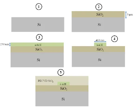
4.1 The process flow for fabrication of devices on a-Si:H-on-insulator substrates.
Step 1/2: Grow 3 µm thick wet oxide on a silicon substrate. Step 3: Deposit 250
nm thick a-Si:H using PECVD. Step 4: Pattern waveguides using e-beam
lithography and etch a-Si:H. Step 5: Deposit 2 is µm thick PECVD SiO2 to
xiv
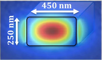
4.2 Mode profile of a fundamental quasi-TE mode in a-Si:H waveguide.. ... 39
4.3 SEM images of fabricated microdisc (left) and microring (right) resonators in
a-Si:H.. ... 39
4.4 Measured transmission spectrum of ring resonators fabricated in a-Si:H. The
measured free spectral range is ~ 20 nm. Inset shows the measured Q-factor to be
~ 8600 based on a Lorentzian fit to the measured spectrum.. ... 40
4.5 Measured response of microdisc resonators fabricated in a-Si:H. The measured
Q-factor is ~ 92,000.. ... 41
4.6 Experimental set-up to demonstrate amplitude modulation in a-Si:H waveguides.
The 405 nm pump pulses are incident on an a-Si:H waveguide to modulate the
1550 nm cw probe light. PC: Polarization Controller.. ... 44
4.7 All-optical modulation in a-Si:H using a pump-probe scheme. The carriers
undergo a rapid thermalization before undergoing non-radiative recombination..45
4.8 In-plane experimental set-up to demonstrate broadband amplitude modulation in
a-Si:H waveguides. The 1540 nm pump pulses are coupled into an a-Si:H
waveguide to modulate the 1560 nm cw probe light. PC: Polarization Controller.
OPO: Optical Parametric Oscillator... 47
4.9 In-plane all-optical modulation in a-Si:H using a pump-probe scheme. The
carriers undergo a rapid thermalization before undergoing non-radiative
xv
4.10 All-optical modulation in a SOI ring resonator using a pump-probe scheme. Inset
shows the transmission spectrum of the ring resonator with the probe signal
wavelength below the resonance wavelength of the ring resonator.. ... 50
5.1 Experimental set-up to measure optical nonlinearities in a-Si:H waveguides.
OPO: Optical Parametric Oscillator, OSA: Optical Spectrum Analyzer.. ... 52
5.2 Output power (black squares) as function of coupled input power for a-Si:H
waveguide. The blue line indicates the fit measured data based on solving the
nonlinear equations.. ... 55
5.3 Modeling fit to measured data using the photon absorption (TSA) and
two-state absorption (TSA) model in a-Si:H waveguide.. ... 56
5.4 Output power (black squares) as function of coupled input power for SOI
waveguide. The blue line indicates the fit measured data based on solving the
nonlinear equations.. ... 57
5.5 Measured spectral broadening in a-Si:H waveguides at different coupled powers
due to self phase modulation and modeling fits based on solving nonlinear
Schrödinger equations.. ... 60
5.6 Measured spectral broadening in SOI waveguides at different coupled powers
due to self phase modulation and modeling fits based on solving nonlinear
Schrödinger equations.. ... 61
5.7 Experimental set-up to characterize four-wave mixing in a-Si:H waveguides.. .. 62
5.8 FWM output spectrum measured after a-Si:H waveguide with 16 mW pump
xvi
5.9 FWM in a-Si:H as function of pump power.. ... 64
5.10 Linear change in phase of the idler frequency with increasing pump powers in
a-Si:H waveguides.. ... 65
6.1 Principle of operation of the device is illustrated: (a) two unmodulated ring
resonators result in amplitude level 1. (b) Modulating one ring (blue) resonator
independently results in amplitude level 2 and (c) modulating both resonators
results in amplitude level 3.. ... 69
6.2 Process flow in the fabrication of a-Si:H microring resonators with resistive
heaters. Step 1: 3 µm thick thermal oxide is grown on a silicon substrate. Step 2:
250 nm thick a-Si:H film is deposited using PECVD. Step 3: Waveguides are
patterned on a-Si:H using e-beam lithography. Step 4: 600 nm thick PECVD
SiO2 is deposited to protect the optical mode. Step 5: 80 nm thick Ni-Cr resistive
heaters are patterned using optical lithography.. ... 71
6.3 a) SEM image of the fabricated device. (b) Optical microscope image of the
device with heaters.. ... 72
6.4 Experimental set-up to measure simultaneous thermo-optic switching of two ring
resonators. The two rings are switched individually using the thermo-optic effect
by applying square wave electrical pulses at 100 Hz to produce modulated signal
observed on an oscilloscope... 72
6.5 Thermal tuning of resonator wavelengths is achieved by applying heat to the
xvii
6.6 (a) Temporal response of the system due to modulation of one resonator. The
other resonator is always on resonance. (b). Modulating both resonators
generates three amplitude levels on a single carrier.. ... 74
6.7 Measurement set-up to generate all-optically modulated ASK signals. Two pump
pulses are delayed by 200 ps to enable the demonstration of three switching
levels. PC: Polarization Controller.. ... 75
6.8 (a) The resonances of the individual resonators and through port of the entire
system. The probe wavelength used is slightly blue-shifted off-resonance. (b)
Three level temporal response of the system by switching two ring resonators
with a 200 ps delay.. ... 76
7.1 Schematic layout of a p-i-n diode based on a a-Si:H modulator. The p and n
doped regions are 100 nm in thickness.. ... 80
7.2 Application of a reverse bias across the p-i-n junction results in a decrease of the
free carrier lifetime of the carriers in a-Si:H. An exponential fit results in a
carrier lifetime of ~ 100 ps at 16 V applied reverse bias.. ... 80
7.3 Change in propagation loss in a-Si:H films post-annealing in nitrogen ambience..82
7.4 Fourier Transform Infrared Spectroscope (FTIR) measurements on two
1
CHAPTER 1
INTRODUCTION
1.1
Electrical Interconnects vs. Optical Interconnects
Silicon Photonics can be broadly defined as the use of silicon based materials to
generate, control, transfer, and detect light over a distance to enable communications in
chip multiprocessors (CMPs) [1]. The motivation for silicon photonics as a medium for
optical interconnects (OI) is driven by the power and delay limitations predicted in
copper based electrical interconnects (EI). As device sizes have shrunk with Moore’s
Law as a general rule, ultra-short distance communications on chips have mostly been
dominated by electrical interconnects due to the relative ease in their design and
fabrication, as well as tolerable power and delay requirements at remarkably low cost.
The older 1.0 µm Al/SiO2 technology generation had transistor delays on the order of 20
ps and RC delays of 1 ps/mm. With scaling to finer technology nodes due to innovations
in lithography, the 35 nm Cu/low-κ transistors are expected to have transistor delays of 1
ps [2].
However, as processor speeds increase, it is becoming more difficult to keep a
balance between logic operations (i.e. floating point operations or FLOPS) on the chips
and the read/write operations of bytes of information into and out of memory. A good
rule of thumb is to keep a ratio of 1 byte/FLOP [3]. However, modern systems cannot
achieve anything close to this ratio. Current predictions for electrical interconnects
indicate this ratio is going to get progressively smaller due to limitations on wiring.
The RC delays in electrical interconnect based devices are predicted to be 250
2
expense of smaller bandwidth density. However, it is predicted that minimum achievable
delay shall reach a limit at 20 ps/mm despite a scaling towards finer technology nodes
seen here in Figure 1 [4].
Figure 1.1 Propagation delay in Electrical Interconnects as a function of normalized interconnect width for different technology nodes [4].
Optical interconnects (OI) are proposed as an alternate solution for on-chip
communications. This is due to their speed of light propagation and large bandwidth due
to the high frequency of optical signals, of the order of 200 – 1000 THz for the
corresponding free-space wavelengths of ~ 1.5 µm to 300 nm. The short wavelength of
light enables the use of dielectric waveguides to guide these waves with very low
transmission losses. The minimal interaction between photons leads to minimal
cross-talk between signals being transmitted. Thus optical interconnects have a significant
advantage over the undesirable cross-talk generated in metal-dielectricinterconnects. Due
[image:20.612.154.499.158.426.2]3
delay over electrical interconnects. Electrical signals, however, have to be converted to
optical signals to utilize the propagation speeds offered in OIs and have to be converted
back into electrical signals for further processing. This conversion requires a fixed
amount of delay which is independent of the interconnect distance [4]. It has also been
shown that on-chip optical interconnects can achieve lower power and latency than their
electronic counterparts when the interconnect length is greater than 1000 times the
wavelength [5]. Therefore, optical interconnects tend to have an advantage over
electronic interconnects over long communication distances as seen in Figure 2, where a
comparison between cu/low-κ electrical interconnect and a silicon waveguide optical
interconnect is shown [4]. In keeping with these trends, the International Technology
Roadmap for Semiconductors (2007, Interconnects) envisions the integration of optical
interconnects for long communications in upper metal layers of CMOS fabrication
process.
[image:21.612.168.481.435.690.2]4
1.2. Hybrid Photonic-Electronic Networks-on-Chip Architecture
Networks-on-chip (NoCs) have been proposed to replace the traditional electrical busses
[6,7]. Although electronic NoCs have demonstrated some improvements in bandwidth
and latency, power consumption remains a critical issue because of high switching
activity in electrical interconnects [8,9]. The application of photonics to NoCs is
projected to be a more attractive method in simultaneously achieving low power
consumption, low latency, and high bandwidth [10]. Recently, a global on-chip optical
bus has been applied to remote memory access paths in a multi-core processor [11]. The
bus successfully obtained 50% latency reduction over some applications and about 30%
power reduction over a baseline electrical bus. A hybrid photonic NoC integrating a
photonic circuit-switched network for message transmission and electronic
packet-switching for routing path set-up has been presented as well [12]. Based on the strengths
of these works, a multicore chip architecture utilizing a hybrid electronic-photonic
network is proposed to achieve low power, low latency, high bandwidth and reliable
interconnection between cores. Figure 1.3 shows the CMP cores arranged in a grid
5
Figure 1.3 Hybrid NoC architecture. The cores are connected to the hybrid photonic-electronic NoC by gateway switches that inject and eject photonic and photonic-electronic packets into the network.
To illustrate the operation of a hybrid NoC, the path taken by a typical message
between two cores on the chip is described. After the core determines the amount of data
to be transmitted to another core over the photonic NoC, an electronic path setup packet
containing the source and destination address, photonic message length, error information
and priority information is broadcast over the electronic network. To enable the data to be
routed across the network, photonic routers are reconfigured while the packet propagates
through the network. If a path cannot be established, a message is sent back to the source
indicating a bottleneck in the network. If no contentions occur during the path setup, the
destination sends an acknowledgement over the photonic network. The photonic path
being bi-directional automatically propagates the acknowledgement back to the source.
6
1.3. Silicon-based Photonic Interconnects
In a hybrid network-on-chip (NoC) architecture, the issue of where to integrate photonic
circuits into electronic IC fabrication processes to achieve maximum flexibility and
minimize complexity and cost is an important one. The backend integration of photonic
components in the upper metal layers of CMOS fabrication process is an envisioned
solution. The compatibility of silicon photonics with complementary metal-oxide
semiconductor (CMOS) processes used in the development of electronic processors has
also contributed to its rapid emergence as a cost-effective solution to integrate photonic
and electronic circuits on a single platform. Recent advances have enabled the
demonstration of integrated modulators and detectors that form the core of an optical
interconnect network [13-17]. These devices have primarily been fabricated on single
layer crystalline silicon-on-insulator substrate.
However, with increasing device density on a single layer, the design of future
generations of interconnect networks will be a challenge. Vertical stacking of silicon
layers to form a 3-D hybrid photonic-electronic network-on-chip (NOC) is a proposed
solution to overcome the constraints posed by the device density [10,18]. Photonic
devices on three vertically stacked layers of crystalline silicon have been demonstrated
[19]. The process is fabrication intensive involving multiple implantation and epitaxial
growth processes, and is not likely to be cost effective. More recently, polycrystalline
silicon [20-22] and amorphous silicon [23-26] have been proposed as alternate solutions
for large scale 3D integration of optical interconnect networks.
Although it is a viable solution, polysilicon has higher optical losses due to scattering
7
the thermal budget of the interconnect architecture. To achieve device quality substrates,
polysilicon films need to be annealed at elevated temperatures (>600 C), thereby
increasing the thermal budget. An alternate solution is to anneal amorphous silicon films
with short pulse lasers to form local polycrystalline regions [27]. This process, however,
can add to the complexity of fabrication of the electro-optic NoC architecture. Integrated
optical devices fabricated in deposited silicon crystallized at room temperature have been
measured to have extremely high optical losses [28].
Amorphous silicon is characterized by the absence of long range order in its atomic
structure. This causes the material to have a large density of point defects and dangling
bonds, collectively called coordination defects, caused when an atom has too many or too
few bonds [29]. Addition of hydrogen to amorphous silicon reduces the defect density by
saturating the dangling bonds resulting in a low loss platform for nanophotonics.
Hydrogenated amorphous silicon (a-Si:H) can be deposited using low temperature
(~250-400 ºC) plasma-enhanced chemical vapor deposition (PECVD) which is automatically
compatible with the backend thermal budget in the CMOS fabrication process.
Therefore, amorphous silicon can be integrated at any point in the fabrication process
with minimal complexity. This makes hydrogenated amorphous silicon (a-Si:H) a
material of choice in the backend integration of a hybrid NoC.
A proposed hybrid photonic-electronic multicore chip using a-Si:H is shown in
Figure 4. The transistors reside on the bottom layer and will further be connected to the
photonic circuits through the metallization stack. The photonic circuit primarily consists
of 0.46 µm by 0.25 µm cross section amorphous silicon ‘wires’. The photonic wires are
8
bends. However, they are fundamentally different since they do not require any power to
propagate the signal. Once the light is coupled in these wires, it will freely propagate at
the speed of light and can intersect with other wires with minimal interference between
signals. Also seen in this cross-section are lasers and SiGe photodetectors whose
implementation on chip has been proposed by others [30].
Figure 1.4 Cross section of a proposed hybrid photonic-electronic chip. The structure is based on SOI with embedded SiGe regions for transistor strain, growing laser materials, and for photodetectors. Hydrogenated amorphous silicon wires (a-Si:H) are integrated in the metal stack and used to transfer light throughout the chip. Multiple a-Si layers are used for transferring light from layer-to-layer.
The proposed research in this thesis will characterize hydrogenated amorphous silicon
(a-Si:H) waveguides for its feasibility as photonic platform in its integration in a hybrid
9
CHAPTER 2
HYDROGENATED AMORPHOUS SILICON
2.1 Atomic Structure in Amorphous silicon (a-Si)
Silicon is currently the most attractive material of choice for electronic devices
because of its abundance and unique semiconducting properties. It is used to make
transistors and integrated circuits used in the computer industry, flat-panel displays, and
solar-cell applications. Silicon exists in monocrystalline, polycrystalline, and amorphous
forms. Monocrystalline or single-crystal Si consists of an unbroken, continuous crystal
lattice structure with no grain boundaries. Polycrystalline silicon consists of multiple
small silicon crystals that are connected together by grain boundaries. Amorphous silicon
on the other hand is the non-crystalline form of silicon. In amorphous silicon, there is an
absence of any long range order, and an emphasis is placed on short-range coordination
bonds [29].
The disorder of the atomic structure is the main feature that distinguishes amorphous
silicon from its crystalline counterpart. The short range order and long range disorder
lead to a model of continuous random network as shown in Figure 2.1. The periodic
crystalline structure is replaced by a random network where each atom has a specific
number of bonds to its immediate neighbor called coordination bonds. This random
network can easily incorporate atoms of different coordination even in small
concentrations. This contrasts with the crystalline nature of silicon where impurities are
constrained to have the coordination of the host because of long range ordering of the
lattice. The short range ordering in amorphous silicon manifests as the elementary defect
10
Figure 2.1 Continuous random network containing atoms of different bonding coordination
[29].
Figure 2.2 Illustration showing the different types of defects in (a) crystalline and (b) amorphous silicon [29].
In crystalline silicon, any atom that is out of place in the crystal is a defect. The
simplest defects in c-Si are vacancies and interstitials as seen in Figure 2.2 (a). The
ability of the disordered network on a-Si to adapt to any atomic coordination allows for
11
2.2 Electronic Structure in Amorphous silicon (a-Si)
The fundamental property of a semiconductor is its band gap structure that separates
the occupied valence band from the empty conduction band. The band gap is a
consequence of the periodicity of the crystalline lattice as defined by the free electron
theory. The bands are influenced strongly by the short range order in both crystalline and
amorphous silicon and the absence of periodicity in a-Si acts as a small perturbation.
The principal features of a-Si are defined by its short range order, long range disorder
and the coordination defects. Short range order results in similar electronic structure in
the case of crystalline and amorphous silicon. However, the abrupt edges in crystalline
silicon are replaced by a broadened tail of states in amorphous silicon that extend into the
forbidden gap that originates from bong length and angle deviations arising from long
range disorder as seen in Figure 2.3 [29].
Figure 2.3 Schematic showing the density of states distribution for amorphous silicon with band, band tails and defect states in the band gap. The dashed curves represent the equivalent density of states in a crystal [29].
The band tails play an important role because the electronic transport occurs at the
12
from the ideal network. These defect states determine many electronic properties by
controlling the trapping and recombination of carriers. The broadened tail states that
result due to deviations cause carrier localization which in turn strongly scatters the
carriers. The strong scattering of the carriers results in lower carrier mobilities in
amorphous silicon (< 10 cm2/V·s) and causes the profound effect of localizing the wave
function. The disorder in the structure in amorphous silicon also manifests in the loss of
momentum (k) conservation in electronic transitions. There is a greater emphasis on the
spatial location of the carrier than on its momentum. It also results in the loss of
distinction between a direct and indirect band gap in amorphous silicon. Instead the
transitions occur between states which overlap in space. Therefore in pure a-Si, many
silicon atoms are three-fold coordinated which leaves one dangling bond. The dangling
bonds are considered to be the most major defect from the localized states in the middle
of the band gap [29]. The density of these defects in pure a-Si (> 1019 cm-3) makes them a
high loss platform for optical waveguides. The first a-Si waveguides patterned using Xe
ion irradiation and reactive ion sputtering had measured losses of ~500 dB/cm and ~30
dB/cm respectively [24].
However, addition of hydrogen to amorphous silicon reduces the defect density and
results in a low loss platform for photonic devices.
2.3 Hydrogenated Amorphous Silicon (a-Si:H)
The incorporation of hydrogen during growth of amorphous silicon results in the
passivation of the dangling bonds and reduces the density of midgap states to ~ 1015 –
13
features of the a-Si:H depend on the details of the deposition process and therefore the
properties of the film vary with the growth conditions.
The usual method of deposition a-Si:H is by plasma decomposition of silane gas,
SiH4, in the presence of an inert gas. Silane can decompose in the absence of plasma at
temperatures above 450 ºC, but the films deposited tend to be mostly of low quality
because the temperature is too high to retain hydrogen. The decomposition of
hydrogenated amorphous silicon films at lower temperatures requires a source of energy
to dissociate the silane molecule which is performed by the plasma.
The first plasma deposition system for amorphous silicon was developed by Chittick
et al and was a radio frequency (rf) inductive system in which an induction coil outside
the quartz deposition chamber created the plasma. Most subsequent designs have
incorporated a diode configuration in which the plasma is contained between two parallel
plate electrodes. Deposition takes place at a pressure of 0.1-3 Torr, which is the optimum
pressure to sustain the plasma. The reactor consists of a gas inlet, the deposition chamber
to hold the substrate, pumping system and source power for the discharge. The deposition
process is referred to as plasma enhanced chemical vapor deposition (PECVD).
The deposition parameters must be varied to obtain a device quality film. The
variation in the gas pressure determines the mean free path for collisions of the gas
molecules and influences whether the reaction occurs in the gas or at the growing surface.
The gas flow rate determines the residence time of the gas species in the reactor. The
variation in the rf power controls the rate of gas dissociation and thereby the deposition
rate of the film. The chemical reactions on the surface are determined by the temperature
14
The hydrogen content during the deposition process ranges from 8 to 40 % and
decreases as the substrate temperature rises. The defect density also depends on the
substrate temperature and rf power and varies by more than a factor of 1000. The lowest
values are obtained at a temperature between 250 – 400º C and are the conditions for
[image:32.612.231.412.214.420.2]films with useful optical and electronic properties.
Figure 2.4 Variation in the hydrogen content in amorphous silicon with substrate temperature
[29].
[image:32.612.248.405.473.664.2]15
Thus, addition of hydrogen during deposition process reduces the defect density states in
16
CHAPTER 3
BACKGROUND AND RESEARCH OBJECTIVES
3.1 Hydrogenated-amorphous silicon (a-Si:H) based planar waveguides
Interest in hydrogenated-amorphous silicon as a material for the realization of optical
interconnects in integrated circuits was initially proposed with the demonstration of a
thermo-optically tunable a-si:H planar waveguide based Fabry-Perot intensity modulator
with > 0.7 dB/cm transmission losses [31]. The hydrogenated amorphous silicon films
were deposited using plasma-enhanced chemical vapor deposition technique (PECVD).
Since then, there have been numerous demonstrations of passive, low loss, planar
waveguides in a-Si:H with emphasis on developing a low cost, CMOS compatible
process for integrating a-Si:H planar waveguides in photonic integrated circuits. Initially,
MeV level Xe ion irradiation of silicon-on-insulator (SOI), followed by annealing of the
substrate in hydrogen ambient was used to define a-Si:H waveguides [32]. However, this
process is fabrication intensive, and waveguides that were demonstrated had relatively
high transmission losses. Plasma-enhanced chemical vapor deposition (PECVD) has
since become the de facto standard process for depositing a-Si:H, since nearly all
dangling bonds are passivated with hydrogen. One of the first demonstrations of low loss
17
Table 3.1. PECVD deposition parameters for a-Si:H [33] SiH4 flow 70 sccm
Ar flow 210 sccm
Substrate temperature 300 ºC
Pressure 500 mTorr
RF power 250 W
Frequency 380 kHz
Deposition rate 96 nm/min
The transmission loss in a-Si:H waveguides patterned using the deposition parameters
in Table 3.1 was measured to be < 0.5 dB/cm for multimode waveguides, and < 2 dB/cm
for single mode waveguides at 1550 nm. There have been several other demonstrations of
low-loss planar a-Si:H waveguides based on PECVD [34-36]. More recently, low loss (~
2.5 dB/cm) channel a-Si:H waveguides were demonstrated using a damascene process. A
1 µm thick SiO2 was thermally grown on a silicon substrate and 600 nm wide and 100 nm
deep trenches were defined using standard photolithography, followed by a RIE etch
using CHF3 and CF4 chemistry. A 300 nm hydrogenated amorphous silicon (a-Si:H) film
was then deposited using PECVD to uniformly fill in the trenches. The excess a-Si:H was
polished away using a standard chemical-mechanical polishing process (CMP) as shown
18
Figure 3.1 Angled cross-sectional SEM images of (a) as-etched oxide trenches before
photoresist (PR) is removed; (b) overview of a racetrack resonator after CMP; (c) a-Si channel waveguide formed in the oxide trench after CMP; (d) coupling region of the racetrack resonator after CMP [35].
Planar waveguides along with racetrack resonators in a-SI:H were fabricated using
the damascene process. Since the undercladding layer was only 1 µm thick, only TE
polarized modes could be excited in the waveguides as the TM modes were lost to
substrate coupling. The racetrack resonators exhibited quality factors (Q) in the range of
mid 104 – 105 as shown in Figure 3.2.
Figure 3.2 The measured quality factors in the a-Si:H racetrack resonators fabricated using
19
3.2 Modulation Schemes in a-Si:H waveguides
Thermo-optic and all-optical modulation schemes have also been exploited in a-Si:H
to demonstrate modulation of optical signals in planar waveguides. The thermo-optic
coefficient has been determined to be 2.3·10-4 K-1 which is 20% higher than in crystalline
silicon [37]. Hydrogenated amorphous silicon film was stacked between two layers of
hydrogenated amorphous silicon carbide films to form a planar waveguide as shown in
Figure 3.3 and glued to a Peltier heat pump. The transmitted light intensity was
monitored in the temperature range between 30 ºC – 40 ºC [37].
Figure 3.3 A planar a-Si:H waveguide with a-SiC:H films forming the top and bottom
cladding layers [37]
The recorded transmitted intensity (It) plotted against the change in temperature is
shown in Figure 3.4. The periodic amplitude modulation is because of setting up
instigating interference patterns in the waveguide that acts a Fabry-Perot resonant cavity.
The change in refractive index due to the change in temperature results in the tuning and
[image:37.612.245.405.300.474.2]20
Figure 3.4 Thermo-optic modulation of light in a planar a-Si:H waveguide [37].
All-optical modulation of light in a-Si:H planar waveguides has also been
demonstrated [38]. A boron doped a-Si:H film was deposited on top on a silicon substrate
with ZnO serving as the cladding region. The waveguides were 4 mm wide and 1.75 µm
thick. The pump-probe setup is shown in Figure 3.5 (a).
Figure 3.5 (a) The configuration between pump and the probe is schematized. (b) Modulation
depth M measurements on the a-Si:H waveguide vs. the pump illumination intensity at each pump wavelength [38].
The probe beam at λ = 1.55 µm was incident orthogonally to the waveguide and was
modulated using pump beam from AlInGaP light emitting diodes (LEDs) at different
21
change in the modulation depth (M) of the probe signal indicates a photoinduced infrared
absorption modulation of the probe signal.
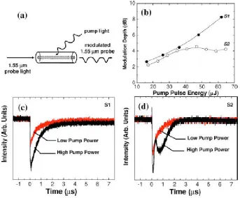
More recently, all-optical modulation in amorphous silicon filled microstructured
fibers was demonstrated as shown in Figure 3.6 [39]. The fiber pores, 6 µm in diameter,
were filled with a-Si:H by heating the fibers to 480-496 ºC and flowing a precursor of
SiH4 and He gases. The propagation losses in the fibers were estimated to be 24.8 dB/cm
and 17 dB/cm. The probe signal at λ=1.55 µm was illuminated with a pump pulse at 532
nm, (17.5 ns width, 10 Hz repetition rate) and the temporal response measured as shown
below.
Figure 3.6 (a) Schematic diagram of the all-optical modulation setup in a-Si:H filled
[image:39.612.151.494.328.612.2]22
Based on the measured temporal response, the effective carrier lifetime in the
amorphous-silicon filled microstructured fibers was measured to be 690 ns.
Electro-optic effects in a-Si:H have not been demonstrated much because of the weak
quadratic electro optic effect and the difficulty in achieving a significant carrier injection
across p-n junctions, due to the low mobility values of the carriers in hydrogenated
amorphous silicon [40, 41].
A modest absorption modulation scheme has been demonstrated, based on depositing
a multilayer alternating stack of hydrogenated amorphous silicon (a-Si:H) and amorphous
silicon carbonitride (a-SiCxNy) on a heavily p-doped silicon substrate as shown in Figure
3.7 below [42].
Figure 3.7 Schematic cross sections of realized planar waveguides and corresponding
refractive index profiles. The crystalline silicon substrate is 300 µm thick [42].
The deposited a-Si:H layers were 1 µm thick and the a-SiCN layers were 30 nm in
thickness. A strong vertical confinement of the optical mode is achieved due to the high
index difference between the two films, ∆n ~ 2. A 100 nm thick, transparent indium tin
oxide (ITO) forms the top contact and the silicon substrate forms the bottom contact. The
presence of a-SiCN layers between a-Si:H creates a capacitive effect and causes a
23
obtained for the three bi-layers sample (L = 1.2 cm) and a modulation depth of 27% is
obtained for the six bi-layers sample (L = 1.5 cm). The effective absorption co-efficient
(∆α) was measured to be 0.11, 0.18 and 0.21 cm-1 at 10, 20 and 30 V biases respectively
corresponding to an electric field of 0.15, 0.30 and 0.45 MV/cm across the insulating
a-SiCN layers. The change in the optical output with respect to applied signal is shown in
Figure 3.8 (a) below. The modulation depth with respect to frequency for the six bi-layer
structure driven by 20 V pulses is shown in Figure 3.8 (b). The modulation bandwidth is
limited by the characteristic carrier recombination times due to carrier trapping and
releasing in shallow levels in disordered a-Si:H films. An enhancement of the modulation
can be achieved by increasing the number of a-Si:H/a-SiCN layers in the stack and by
thinning the stack as both approaches increase the relative volume of the waveguide
where carrier accumulation takes place, and should also allow for a reduction in the
applied bias voltages. This scheme is the only active electro-optical device demonstrated
in a-Si:H.
Figure 3.8 (a) Output light power and applied voltage for a six bi-layer 1-cm long
waveguide. The modulating signal has Vmin = 0 V, Vmax = 15 V, duty cycle = 50 %,
24
3.3 Optical Nonlinearities in a-Si:H Waveguides
Enhanced optical nonlinearities have been measured in amorphous silicon films using
a z-scan measurement technique, shown here in Figure 3.9 [43]. A comparison of the
nonlinearities was made between crystalline silicon, amorphous silicon, and two
hydrogenated amorphous silicon films. The amorphous silicon film was deposited using
RF sputtering technique, while the hydrogenated amorphous silicon films were deposited
using PECVD.
A qualitative description of the samples used in the experiments in given in Table 2
below. To quantify the nonlinearities, an enhanced nonlinear co-efficient β’ was defined
by combining the two-photon absorption co-efficient β of crystalline silicon and
free-carrier cross section σ.
25
Table 3.2. Material properties and parameters for a-Si:H [43]
p
τ
π
ω
α
σ
β
β
2
ln
2
2
'
h
+
=
The nonlinear coefficients β’s were calculated to be 104 cm/GW for a-si, 6.7 cm/GW for
a-Si:H (1) and 1.4 cm/GW for a-Si:H(2). The enhanced nonlinear absorption is attributed
to a “two-step absorption” (TSA) from mid-gap localized states as shown in Figure 3.10.
Figure 3.10 Schematic diagram describing two-step absorption (TSA) through mid-gap localized
states [43].
There has been no measurement of the nonlinear refractive index n2 in a-Si:H to the
26
In conclusion, this section reveals previous progress made in the field of amorphous
silicon photonics (a-Si:H). Low-loss planar waveguides and microresonators have been
demonstrated to achieve passive routing of optical signals. However, there is a need for
the characterization of the nonlinear properties in a-Si:H, as well as the demonstration of
an efficient electro-optic modulator that can enable active devices to route signals in an
interconnect network.
3.4 Research Objectives
The primary goal of this thesis is to investigate the feasibility of hydrogenated
amorphous silicon (a-Si:H) as an alternate platform to crystalline silicon, enabling
backend integration of optical interconnects in a hybrid photonic-electronic
network-on-chip architecture. We shall now give an outline of the thesis focusing on results achieved
towards reaching the end goal and describe the theory behind the results obtained.
3.5 Thesis Outline
3.5.1 Passive Microcavities
In Chapter 4, we demonstrate a low-loss hydrogenated-amorphous silicon (a-Si:H)
platform, along with high quality factor micro-cavity devices that can enable the
realization of on-chip wavelength-division multiplexing schemes. We also demonstrate a
broadband all-optical modulation scheme in a-Si:H based on free-carrier absorption
effect in stark contrast to band-limited modulation schemes using cavity resonators
based on free-carrier plasma dispersion effect observed in crystalline silicon.
The micro-cavities described in Chapter 4 are sub-micron sized waveguides looped
around to form a ring or a donut shaped structure. The optical modes traveling in these
27
certain wavelengths that satisfy the condition described in Equation 3.1, the modes
traveling inside the cavities interfere constructively to build up intensity inside these
structures. The wavelength satisfying this condition is called the resonant wavelength.
M
⋅ = ⋅ ⋅ ⋅
λ
2
π
R n
eff (3.1)In Equation 3.1, R is radius of the cavity, neff is the effective index of the mode traveling
in the cavity, λ is the wavelength and M is the mode number. At all other wavelengths,
modes interfere destructively such that there is no build-up of intensity in these
structures. The transfer function of a micro resonator is shown in Figure 3.11.
Figure 3.11 Transmission spectrum of a microring resonator. The resonance wavelength is indicated
as λ0 and ∆λ is full-width half maximum bandwidth of the resonator.
The full-width half maximum bandwidth defines the quality factor (Q) of the resonators.
The Q-factor of a resonator is defined in Equation 3.2.
28
The sharpness of the resonance or the quality factor (Q) determines the photon lifetime of
the cavity given by Equation 3.3.
p
2
Q
c
λ
τ
π
=
⋅ ⋅
(3.3)The group index of a ring resonator can be determined experimentally by measuring the
free-spectral range (FSR) of the device. The free-spectral range is defined as the spatial
distance between two adjacent resonances. The group index (ng) can be determined from
the measured FSR according to Equation 3.4.
2
2
gFSR
n
R
λ
π
=
⋅ ⋅ ⋅
(3.4)The parameters described here are used to characterize the microresonator devices
fabricated in a-Si:H as described in Chapter 4.
3.5.2 Optical Nonlinearities in Waveguides
In chapter 5, we comprehensively characterize the optical nonlinearities in a-Si:H
waveguides and compare the properties with that of crystalline silicon waveguides. The
nonlinearities in a-Si:H are measured to be 5 times that in crystalline silicon waveguides.
Based on the enhanced nonlinearities, we also demonstrate low-power continuous wave
four-wave mixing in a-Si:H waveguides and measure the nonlinearities based on the
observed spectrum.
The need for a higher bandwidth in optical communications necessitates the use of
short pulses to transmit a higher data bit rate. Ultra-short pulses result in high intensities,
leading to the generation of optical nonlinearities due to the long interaction length in the
29
nonlinear two photon absorption (TPA), self-phase modulation (SPM), four-wave mixing
(FWM) have been previously demonstrated [44-50].
Two-Photon Absorption
Two-photon absorption (TPA) is a nonlinear process where two photons are
simultaneously absorbed to generate an electron-hole pair. TPA occurs when the energy
of a photon is less than the bandgap energy but greater than one-half the energy bandgap.
TPA can be classified into two different types – degenerate TPA and non-degenerate
TPA as shown in Figure 3.12.
Pump
Photons λp Eg
Pump Photon λp
Eg
CW photon λs
(a) (b)
CB
VB
CB
VB λp< λs
Figure 3.12 Two-photon absorption processes - (a) Degenerate TPA, (b) Non-Degenerate
TPA
Degenerate TPA is caused by the absorption of two pump photons having the same
frequency, whereas non-degenerate TPA is caused by the absorption of pump and signal
photon. In the case of non-degenerate TPA, λp < λs, so that TPA occurs only if pump
photon is present. Unlike other nonlinear processes such as Four-wave mixing (FWM),
30
TPA cause free carrier absorption (FCA) of the propagating signal, resulting in the
depletion of the pump power. Thus, the process of two-photon absorption causes the
material to act as an optical limiter. However, devices exploiting the nonlinear properties
in silicon require that free carriers generated due to TPA be actively swept out to
minimize the loss of photons. The intensity (I) of the field propagating within a material
is given by the following relation
(
I
N
)
I
dz
dI
TPA
σ
β
α
+
+
−
=
(3.5)where α is the linear transmission loss, βTPA is the two-photon absorption coefficient and
σ is the free carrier absorption cross-section.
Self-Phase Modulation
Self-phase modulation (SPM) is a nonlinear process where the pump pulse
undergoes an alteration in its phase, proportional to its intensity. The phase of the wave is
given by the relation
φ
( ) (
z
=
n
o+
n
2I
)
k
oz
−
ω
t
(3.6)no is the linear refractive index and n2 is the nonlinear or Kerr coefficient. As the pump
pulse propagates through the medium in time, the time derivative of phase leads to a
change in the mean frequency of wavelength of the pulse as illustrated in Figure 3.13.
z
t
I
k
n
t
z
o∂
∂
−
=
∂
∂
−
=
2)
(
φ
ω
31
Figure 3.13 Schematic illustration of SPM in a silicon waveguide
The nonlinearities described above are characterized by propagating ultra-short
optical pulses through the waveguide and modeling the measured data by solving a set of
nonlinear differential equations given by [51-53]
u
u
k
c
i
N
u
A
u
n
c
i
t
u
i
z
u
l c c eff TPA2
2
2
2
2 2 2 22
ω
β
σ
ω
α
β
−
−
−
−
=
∂
∂
+
∂
∂
(3.8) c c eff TPA cN
A
u
h
t
N
τ
ω
β
−
=
∂
∂
2 22
(3.9)where u is the slowly varying field amplitude, β2 is second-order dispersion coefficient,
n2 is nonlinear Kerr coefficient, βTPA is the two-photon absorption coefficient, Aeff is the
effective mode area, Nc is the free carrier density, σ is the free carrier absorption
coefficient, kc is free carrier dispersion coefficient, αl is the linear loss parameter and τc is
the free carrier lifetime. Equations 3.8 and 3.9 are solved using a split-step Fourier
method [54] to model the nonlinear parameters in a-Si:H.
Split-Step Fourier Method
The split-step Fourier method can be better understood by splitting Equation 3.8
32
(
D
N
)
A
z
A
ˆ
ˆ
+
=
∂
∂
(3.10)( )
∂ ∂ − ∂ ∂ + = − ∂ ∂ + ∂ ∂ − = T A T A A T A i A i N T T i D R 2 2 0 2 3 3 3 2 2 2 1 2 6 2ω
γ
α
β
β
) ) (3.11) D )is the differential operator that accounts for dispersion and losses within a linear
medium and N
)
is a nonlinear operator that governs the effect of waveguide nonlinearities
on pulse propagation. In the split-step Fourier method, the solution is obtained based on
the assumption that in propagating the optical field over a small distance h, the dispersive
and nonlinear effects act independently of each other. The propagation from z to z + h is
assumed to be carried out in two steps. In the first step, the nonlinearity acts alone, and
Dˆ = 0 in Equation 3.10. In the second step, the dispersion acts alone, and Nˆ = 0 in
Equation 3.10. Equation 3.10 then evaluates to:
A
(
z+h,T)
≈exp(hDˆ)exp(hNˆ)A(z,T) (3.12)The exponential operator exp(hDˆ)can be evaluated in the Fourier domain using the
relation
exp(hDˆ)B(z,T)=FT−1exp
[
hDˆ(
−iω)
]
FTB( )
z,T (3.13)33
Figure 3.14 Schematic illustration of a symmetric split-step Fourier method used for numerical
modeling. The waveguide length is divided into a large number of segments of width h. Within a
segment, the effect of nonlinearity is included at the mid-plane shown by a dashed line.
(
)
( )
ˆ
)
(
,
)
2
exp(
)
ˆ
exp(
)
ˆ
2
exp(
,
T
h
D
N
z
'dz
'h
D
A
z
T
h
z
A
h z z∫
+≈
+
(3.14)
The split-step Fourier method can be implemented based on Equation 3.14 and Figure
3.14. The waveguide length is divided into a large number of segments that do not have
to be spaced equally. The optical pulse is propagated between each segment according to
Equation 3.14. The pulse is first propagated for a distance h/2 considering dispersion only
using the FFT algorithm of Equation 3.13. At the mid-plane z+h/2, the field is multiplied
by a nonlinear term that represents the effect of the nonlinearity over the length h. Then
the pulse is propagated over the remaining distance h/2 with dispersion only to obtain
A(z+h,T).
Four-Wave Mixing
Signal amplification and wavelength conversion are essential for an integrated
34
necessary to maintain the signal/noise ratio in the system and the ability to transfer data
from an existing signal to a different wavelength has enormous potential in a wavelength
division multiplexed system (WDM). Four-wave mixing (FWM), a third-order nonlinear
parametric process, is capable of achieving both signal amplification as well as
wavelength conversion. Four-wave mixing occurs when photons from one or more waves
are annihilated and new photons are created at different frequencies such that the total
[image:52.612.209.432.281.508.2]momentum and energy of the process are conserved as shown in Figure 3.15.
Figure 3.15 Schematic description of Four-wave mixing (FWM) process.
The creation of the signal and idler waves depends on the degree of phase mismatch
between propagation constants of the waves and the nonlinear effects of self-phase
modulation (SPM) and cross-phase modulation (XPM). The phase matching condition is
given by [54]
35
∆k=k1+k2 −k3−k4 (3.16)
∆k=(n1
ω
1+n2ω
2−n3ω
3−n4ω
4)/c (3.17)where ∆k is the net propagation constant, γ is the nonlinear coefficient, P1, P2 are the
pump powers and ω1, ω2, ω3 and ω4 are the pump, signal and idler frequencies
respectively. Under the condition when the pump powers are equal (P1=P2, ω1=ω2), the
phase matching condition is given as
κ
=
2
γ
P
pump−
∆
k
(3.18)∆k =2kpump −ksignal +kidler (3.19)
If a signal photon propagates along with the pump photons, then the signal photon
undergoes amplification from the four-wave mixing process given by
=
(
γ)
2 −( )
κ 2 2pump
P
g (3.20)
A schematic of wavelength conversion and gain in a-Si:H waveguides is shown in Figure
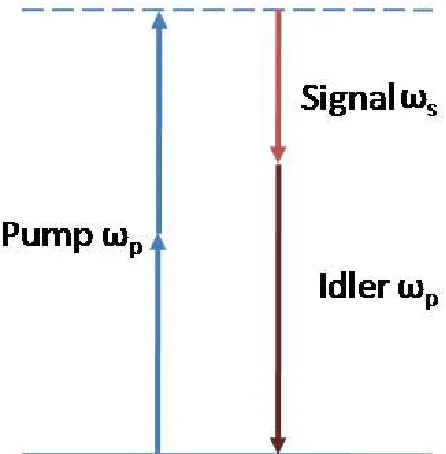
3.16.
Figure 3.16 Schematic of four-wave mixing in a-Si:H with gain and wavelength conversion.
When a strong pump ωp and co-propagating signal ωs are launched in the waveguide, the
refractive index of waveguide is modulated due to the strong nonlinear Kerr effect at the
36
the generation of side-band frequencies ωp ± (ωs-ωp). This results in the signal frequency
ωs causing an amplification of the signal and an ‘idler’ frequency ωi = 2ωp-ωs.
3.5.3 Amplitude-Shift-Keying Modulation in a-Si:H Waveguides
In Chapter 6, we demonstrate a novel data encoding scheme using a system of
ring resonators in a-Si:H to increase the spectral efficiency of an interconnect link.
Thermo-optic modulation of a-Si:H waveguides is utilized to demonstrate a
proof-of-concept three-level data encoding scheme. A high-speed data modulation is also
demonstrated using all-optical modulation of a pair of symmetric ring resonators in
37
CHAPTER 4
ALL-OPTICAL MODULATION IN
HYDROGENATED-AMORPHOUS-SILICON (a-Si:H) WAVEGUIDES
4.1 Deposition of a-Si:H-on-Insulator Substrates
Device quality substrates in hydrogenated-amorphous silicon (a-
![Figure 1.1 Propagation delay in Electrical Interconnects as a function of normalized interconnect width for different technology nodes [4]](https://thumb-us.123doks.com/thumbv2/123dok_us/114022.10838/20.612.154.499.158.426/propagation-electrical-interconnects-function-normalized-interconnect-different-technology.webp)
![Figure 1.2 Propagation delays in cu-based electrical interconnects and silicon based optical interconnects [4]](https://thumb-us.123doks.com/thumbv2/123dok_us/114022.10838/21.612.168.481.435.690/figure-propagation-delays-electrical-interconnects-silicon-optical-interconnects.webp)
![Figure 2.5 Variation in the defect density states with substrate temperature showing an optimum defect density in the 200-300 ⁰C range [29]](https://thumb-us.123doks.com/thumbv2/123dok_us/114022.10838/32.612.231.412.214.420/figure-variation-density-substrate-temperature-showing-optimum-density.webp)
![Figure 3.3 A planar a-Si:H waveguide with a-SiC:H films forming the top and bottom cladding layers [37]](https://thumb-us.123doks.com/thumbv2/123dok_us/114022.10838/37.612.245.405.300.474/figure-planar-waveguide-sic-films-forming-cladding-layers.webp)
![Table 3.2. Material properties and parameters for a-Si:H [43]](https://thumb-us.123doks.com/thumbv2/123dok_us/114022.10838/43.612.268.395.396.580/table-material-properties-parameters-si-h.webp)