Rochester Institute of Technology
RIT Scholar Works
Theses Thesis/Dissertation Collections
2-6-2009
Development and modeling of a low temperature
thin-film CMOS on glass
Robert G. Manley
Follow this and additional works at:http://scholarworks.rit.edu/theses
This Thesis is brought to you for free and open access by the Thesis/Dissertation Collections at RIT Scholar Works. It has been accepted for inclusion in Theses by an authorized administrator of RIT Scholar Works. For more information, please [email protected].
Recommended Citation
D
EVELOPMENT AND
M
ODELING OF A
L
OW
T
EMPERATURE
T
HIN
-F
ILM
CMOS
ON
G
LASS
By
Robert G. Manley
A Thesis Submitted
In Partial Fulfillment
of the Requirements for the Degree of
Master of Science
in
Microelectronic Engineering
Approved by:
Prof:
Dr. Karl D. Hirschman
Prof:
Dr. Michael A. Jackson
Prof:
Dr. Robert J. Bowman
Dr. David F. Dawson-Elli
Dr. J. Greg Couillard
Dr. Carlo A. Kosik-Williams
DEPARTMENT OF MICROELECTRONIC ENGINEERING
COLLEGE OF ENGINEERING
ROCHESTER INSTITUTE OF TECHNOLOGY
ROCHESTER, NEW YORK
D
EVELOPMENT ANDM
ODELING OF AL
OWT
EMPERATURET
HIN-F
ILMCMOS
ONG
LASSBy
Robert G. Manley
I, Robert G. Manley, hereby grant permission to the Wallace Memorial Library of the Rochester Institute of Technology to reproduce this document in whole or in part that any reproduction will not be for commercial use or profit.
A
BSTRACTThe push to develop integrated systems using thin-film transistors (TFT) on
insulating substrates (i.e. glass) has always been limited due to low-mobility
semiconducting films such as amorphous and polycrystalline silicon. Corning
Incorporated is developing a new substrate material known as silicon-on-glass (SiOG). It
is intrinsically better than amorphous and polycrystalline silicon materials due to its
single crystal nature of the silicon film. This however does not mitigate the challenges
associated with low-temperature CMOS process and fabrication.
The first generation of TFTs fabricated at RIT showed the potential of SiOG as a
viable substrate material, but were plagued by considerable short comings such as high
leakage and low transconductance. As part of this study, refinements to TFT processing
on SiOG have demonstrated significant improvement to TFT performance and uniformity,
showing increase transconductanace/mobility, lower subthreshold swing, tighter VT
distributions, and near symmetrical NFET and PFET operation about 0 V. With these
improvements minimal steps have been added to the manufacturing process, keeping
simple and adoptable by the flat panel display (FPD) industry. Device modeling clearly
demonstrates the key areas important to electrical operation, such as dopant activation,
interface charge/trap reduction, and workfunction engineering. It addition, modeling and
simulation have helped to explain the governing physics of device operation explaining
non-ideal effects such as gate induced drain leakage (GIDL) and various mobility
degradation mechanism. An overview of device design, process refinements and device
operation is presented. Process modifications and resulting benefits are discussed along
T
ABLE OFC
ONTENTS
Development and Modeling of a Low Temperature Thin-Film CMOS on Glass ... ii
Abstract ... iii
Table of Contents ... iv
List of Tables ... vi
List of Figures ... vii
Acknowledgments... xii
Chapter 1 ... 1
Introduction ... 1
1.1 Motivation for TFT Advancement ... 1
1.2 Systems-on-Glass Technology Today ... 2
1.3 Thin-film Transistor Designs and Material Systems ... 3
1.4 Partnership with Corning ... 3
1.5 Work Covered by This Document ... 4
Chapter 2 ... 5
Material Systems for Silicon-Based Transistors on Glass ... 5
2.1 Material Systems ... 5
2.2 Amorphous Silicon ... 6
2.3 Polycrystalline Silicon ... 8
2.4 SOI Technology ... 10
2.5 SiOG Material Technology ... 12
Chapter 3 ... 13
SiOG TFT Design and Low-Temperature CMOS ... 13
3.1 Transistor Device Design ... 13
3.2 SiOG Transistor Fabrication Process ... 16
3.3 SiOG Transistor Operation ... 19
Chapter 4 ... 21
Modeling & Simulation of SiOG Thin-Film Transistor Current-Voltage Behavior ... 21
4.3 Thin-Film SiOG PFET design ... 25
4.4 Thin-Film Transistors Designed on SiOG for CMOS ... 27
Chapter 5 ... 36
Process Refinement Towards Improved Device Performance ... 36
5.1 Introduction ... 36
5.2 Surface Finish ... 37
5.3 Cleaning Process Improvements ... 40
5.4 Silicon Layer Design Tradeoffs in SiOG CMOS TFT Performance ... 44
5.5 Enhanced SiOG TFT Performance ... 48
Chapter 6 ... 49
Advanced Device Modeling and Submicron Scaling ... 49
6.1 Introduction ... 49
6.2 Electrical Characteristics of TFTs Fabricated on SiOG and SOI ... 50
6.3 Overlay of Measured and Modeled data ... 52
6.4 Steps toward submicron SiOG TFT scaling ... 56
Chapter 7 ... 69
Conclusion ... 69
7.1 Introduction ... 69
7.2 SiOG Device Design and Simulation ... 69
7.3 Refinement in SiOG processing and improved TFT performance ... 71
7.4 Device Modeling and Understanding ... 73
7.5 Towards SiOG TFT submicron scaling ... 75
7.6 Closing Remarks... 76
Appendix A ... 77
Appendix B ... 83
L
IST OFT
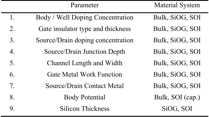
ABLESTable 1. Basic Design parameters for NMOSFETs and PMOSFETs ... 22
Table 2. Summary of SiOG silicon film thicknesses and corresponding dopant concentration. A duplicate wafer at 200 nm thickness was created but had a slightly higher dopant concentration. ... 45
L
IST OFF
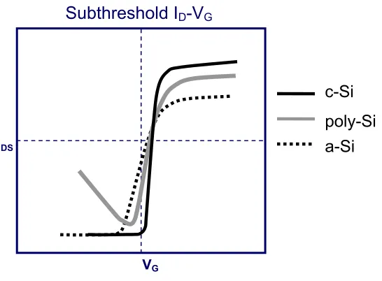
IGURESFigure 1. Schematic of the transfer characteristic for a-Si, poly-Si and crystalline silicon thin-film material systems. SiOG could potentially off higher current drive and less leakage for transistor of the same geometry. ... 6
Figure 2. Cross-section of a typical bottom gate amorphous thin film transistor. ... 8
Figure 3. Schematic of SOI device showing (a) partially depleted device and (b) a fully depleted device ... 10
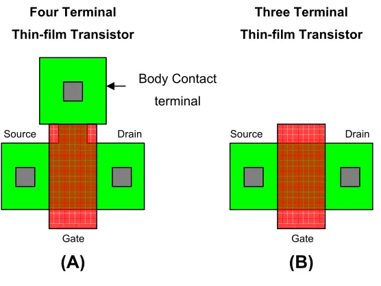
Figure 4. Schematic representation of a (A) four terminal and (B) three terminal thin-film transistor layouts. The body contact of the four terminal transistor is of the same type of dopant as the body of the transistor. Because of the thin film nature of the substrate, the body contact needs to be made laterally on the surface with a terminal that connects the contact and the body region and is protect from any implants that would change its type. By comparison, the three terminal transistor is much simpler and compact. ... 14
Figure 5. Cross-section schematics of SiOG NFET and PFET devices ... 16
Figure 6. Cross-section of a low temperature fabricated SOI FET using deposited dielectric films. For CMOS operation, the NFET and PFET were isolated via a Si mesa etch. ... 19
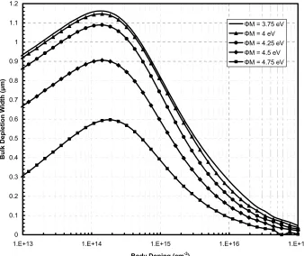
Figure 7. The effect on body doping and gate metal workfunction on the induced depletion width at VGS = 0 V. The maximum depletion with occurs between 1×10¹⁴
and 2×1014 cm-3. Boron concentrations above or below this point cause the depletion width to decrease. At higher boron concentrations there are more dopant ions per unit volume to match charge on the gate and thus the field effect does not need to reach as far. For lower dopant concentrations ... 24
Figure 8. Band Diagrams for Thin-Film PFET on 200 nm p-type Silicon Film Gate Oxide: 50 nm, Molybdenum Gate (ΦM = 4.53 V), NA: 3×1015 cm-3 ... 27
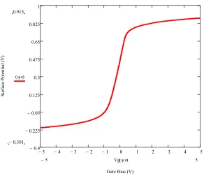
Figure 9. Silicon surface potential as a function of applied gate bias for p-type silicion, NA = 1 ×1015 cm-3, oxide thickness of 50 nm and a Mo gate (ΦMS). ... 28
threshold voltage with a minimal impact on mobility lowering.. (For both devices: XOX = 50 nm and ΦM = 4.53 eV) ... 31
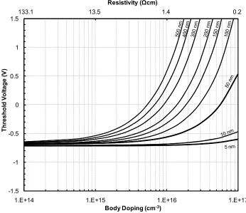
Figure 11 Simulation of the effects of body doping concentration and silicon film thickness on the linearly extroplated threshold voltage of a thin-film accumulation-mode PFET on glass. The threshold voltage is that from a linear extrapolation on an IDS vs. VGS plot. A negative (positive) threshold voltage denotes an enhancement (depletion) mode biasing scheme. A 50 nm gate oxide and molybdenum workfunction of 4.53 eV were used. ... 32
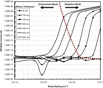
Figure 12. Simulation of the minimum off-state current of the thin-film PFET on glass. The dotted line denotes whether the transistor is operating as an enhancement mode or a depletion mode device (i.e it represents the current at the extracted
threshold voltage). Even if a transistor has an enhancement mode threshold voltage
is still may not have adequate off-state characteristics. If the silicon film is too thick, or the body dopant concentration is too high, there will be a significant amount of leakage current. Current values < 10-15 A are subject to numerical error from the simulation software. ... 33
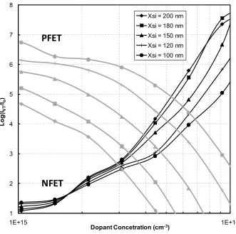
Figure 13. Numerical modeling of design space for NFET and AMPFET transistors on SiOG under ideal conditions; considering no interface charge or trap states. The off-state metric is Log(IVT/Io), described in the text. Devices with a channel length
of 2 µm and a gate oxide thickness of 50 nm were simulated using a molybdenum gate workfunction. Intersecting points of same film thickness represents symmetric operation of both the NFET and AMPFET transistors with threshold voltages of the same magnitude. ... 34
Figure 14. Electron field-effect mobility with varying surface conditions on bulk substrates. The field-effect mobility was extracted from the maximum transconductance from an NFET transistor fabricated on bulk Si with the substrate temperature not exceeding 600 °C. The Alt. #2 finish showed to be far superior to the then standard finish. The ideal surface is resulting from a prime-grade bulk silicon wafer, direct from the manufacturer. ... 38
Figure 15. CV measurement of bulk wafers with different surface finished. Surface finish Alt. #1 is not shown because it did not yield interpretable MOS C-V curves. .... 39
Figure 16. Improved I-V characteristics with Alt. 2 surface finish and improved cleaning process for transistor (L = 6µm, W = 24µm) fabricated in bulk substrates at temperatures ≤600 °C. The characteristics show the same trend, but are slightly offset. Note that the Alt. #2 characteristic presented is a best-case device sample. ... 40
Figure 17. SiOG TFT ID-VG characteristics (L = 3µm and W = 24µm) with two
different cleaning processes prior to the gate SiO2 dielectric deposition. Each
interface traps. The kink observed in the piranha-only NFET transistors has been linked to silicon dangling bonds at the interface through numerical modeling. Implementing the modified RCA clean resulted in a significant reduction in both fixed interface charge and interface trap levels. ... 43
Figure 18. Numerical modeling of SiOG NFEF ID-VG characteristics for devices
that saw the piranha-only cleaning process. Excellent overlay of between the measured and modeled devices is shown. The kink in the characteristics corresponds to a donor-like interface trap 0.8 eV from the conduction band edge. This has been found to correspond to a possible trap state for a silicon dangling bond []. An ideal NFET I-V characteristic is also shown for comparison without any interface traps. ... 44
Figure 19. MOSFET threshold voltage as a function of SiOG silicon thickness. A linear trend should be observed. At the 150 nm thickness treatment, a slight deviation from the trend is observed, both the NFET and PFET threshold voltage have a lower magnitude threshold voltage. This is consistent with a lower P-type film dopant concentration. ... 46
Figure 20. NFET and PFET current drive as a function of silicon thickness. The PFET trend follows expected behavior, showing more current as the p-type silicon layer thickness is increased. The NFET demonstrates a peak current drive at a p-type silicon film thickness of 200nm, with an apparent compromise in carrier mobility as the film thickness is decreased further due to the thinning process. ... 47
Figure 21. A comparison of SiOG and SOI TFTs fabricated at low temperature. Multiple devices are shown (n = 9) to give an indication of uniformity. Implementing surface finish and cleaning improves allowed for a considerable improvement in SiOG NFET and PFET I-V performance and uniformity across a 4-inch substrate. Transistor operation at VDS = 0.1 V and 5 V are shown. L=6 µm,
W=24 µm, and the gate SiO2 thickness was 50 nm. A further discussion on device
characteristics is presented in Chapter 6. ... 48
Figure 22. A comparison I-V characteristics of TFTs fabricated on SiOG and SOI for |VDS| = 0.1V and |VDS| = 5 V. Both substrates show GIDL at the higher drain
bias condition; however it is considerably higher with the SiOG transistors. ... 50
Figure 23. Distributions of interface charge at the silicon/glass interface as derived through numerical modeling and simulation. Through this analysis, it appears that the backside interface is dominated by acceptor-like trap states in the off-state where EF is moving towards EC. ... 53
Figure 24. Overlay of modeled characteristics with measured SiOG transistor data. on a linear current scale. |VDS| = 5 V and L = 6 µm to ensure long-channel behavior.
The following primitive device parameter values were used: ΦMS = 4.53 eV, Xox =
48 nm (measured optically), XSi = 200 nm, NA = 3×1015 cm-3. Low-field (SPICE
/V-sec for the NFET and AMPFET, respectively. See the text for additional details on numerical model enhancements. ... 54
Figure 25. Overlay of modeled characteristics with measured SiOG transistor data with |VDS| = 5 V and L = 6 µm to ensure long-channel behavior. ... 56
Figure 26. Measured saturation-mode (VDS = -5.0 V) VT roll-off characteristic of
the SiOG AMPFET. The relatively small VT offset at L = 2 µm is expected due to
the device parameters chosen based on the design tradeoffs involved in the NFET and AMPFET for CMOS operation. ... 58
Figure 27. Body adjust implant implemented on a thin-film NFET transistors. A 5.5×1011 cm-2 boron dose, a 6.5×1011 cm-2 phosphorus does we performed and compared to an NFET transistor that did not receive any body adjust implant. With no implant and a P-type substrate dopant concentration of 3×1015 cm-3 resulted in a 0.3 V threshold voltage. The boron implant increase the threshold voltage to 1.15 V while the phosphorus implanted lowered it to -1.33 V. ... 62
Figure 28. Subthreshold characteristics of those shown in Figure 27. The phosphorous body adjust implant caused a linear left shift in the I-V characteristics. The boron body adjust implant caused a right shift and also degraded the subthreshold slope. A kink in this curve is also present. The degradation of the this curve suggests the implant caused damage that could not be repaired by the low temperature anneal. ... 64
Figure 29. Body adjust implant implemented on a thin-film PFET. A 5.5×1011 cm-2 boron dose, a 6.5×1011 cm-2 phosphorous does we performed and compared to an PFET transistor that did not receive any body adjust implant. With no implant and a P-type substrate dopant concentration of 3×1015 cm-3 resulted in a -0.91 V threshold voltage. The boron implant increase the threshold voltage to -0.05 V while the phosphorous implanted lowered it to -2.38 V. ... 65
Figure 30. Subthreshold I-V characteristics of the thin-film PFET. The boron implant increased the threshold voltage causing a linear shift in the characteristics. However, the minimum off-state is lower because the added boron in the body regions does not allow the gate to deplete this region and effectively. The phosphorous implant lowered the threshold voltage and degraded the subthreshold swing. ... 66
Figure 31. Comparison of C-V characteristics for a thin-film (two dimensional) capacitor on p-type SiOG at 100 kHz with a P+ contacts and N+ contacts. Because of the thin film nature the capacitance quickly goes to zero once the film is fully depleted. ... 68
Figure 33. SiOG TFT ID-VG characteristics (L = 3µm and W = 24µm) with two
different cleaning processes prior to the gate SiO2 dielectric deposition. Each
cleaning process is represented by measurements taken from two devices. The SiOG substrate cleaned only with the piranha shows evidence of threshold voltage shifting due to fixed interface charge and changes in the sub-threshold swing due to interface traps. Reproduced from Figure 17. ... 72
Figure 34. Enhanced TFT performance on SiOG compared to equivalent transistor fabricated on SOI at low temperatures. Reproduced from data in Figure 21. ... 73
A
CKNOWLEDGMENTSI would like to acknowledge all those who helped in some way to complete this study.
First and foremost I would like to thank my advisor, Dr. Karl Hirschman, for all his
support throughout this project. I would also like to thank my committee members,
Dr. Robert Bowman and Dr. Michael Jackson guidance and support. I especially
acknowledge Corning, Inc., particularly David Dawson-Elli, Greg Couillard, and
Carlo Kosik-Williams. Without their support this project would not be possible. The
C
HAPTER1
I
NTRODUCTION1.1 Motivation for TFT Advancement
In the past decade an increased use of thin-film transistors (TFTs) has orcured in
display applications. TFT liquid crystal displays (LCD) and organic light emitting diodes
(OLED) are now found in a variety of fields ranging from large format applications for
televisions and monitors to portable applications for cells phones and digital cameras.
In early LCD technology, passive matrix addressing was used to address each
segment or pixel of the display. These displays were small and low resolution. In the late
1980s attempts to make higher resolution displays were made, however these displays
were plagued by a slow response time and poor contrast. To further increase the contrast,
resolution and size of LCD displays, active matrix addressing was implemented to
address pixels more quickly without the sacrifice of image quality. Active matrix LCD
(AMLCD) and Active Matrix OLED (AMOLED) displays utilize transistors fabricated in
a semiconductor material on the backplane of a flat panel display (FPD). Thus,
addressing is done to each pixel transistor rather than to pixel capacitors directly,
drastically decreasing response time, especially in larger format displays [1].
Today in active matrix displays, the pixels themselves consist of the pixel capacitor,
are fabricated in traditional bulk silicon CMOS technologies. The dominant TFT
transistor technologies today are based in either amorphous silicon (a-Si) or
polycrystalline silicon (poly-Si). The transistor performance characteristics of these
technologies are such that they can easily meet the requirements for controlling pixels [2],
however, they do not deliver acceptable performance for addressing and image
processing. A push is being made to further integrate electronics on FPDs. The poor
performance of devices fabricated in a-Si does not allow for any integrated electronics.
Lower level integration of electronics using long grain polysilicon films has shown some
success. However, the integration using poly-Si has been limited to simple circuits such
as row and column drivers and some small timing circuits [3].
1.2 Systems-on-Glass Technology Today
In FPD industry, there is a push to integrate more circuitry on the display itself,
particularly for small format displays. The goal of system on panel is to develop a fully
integrated display with all required circuitry on the display substrate; data and power
being the only external connections. Technologies utilizing a-Si and poly-Si do not offer
acceptable transistor performance for complex circuitry.
Transistors fabricated in a-Si are plagued by low mobility due to the non-crystalline
nature of the film. Though high device uniformity can be fabricated with this film, the
device performance basically limits the use of transistor fabricated to pixel drivers. On
the other hand, low temperature polysilicon (LTPS) material does offer potentially higher
technology, where the silicon layer is single crystal, transistor performing close to that
fabricated in bulk silicon can be fabricated, offering greater potential for integration.
1.3 Thin-film Transistor Designs and Material Systems
The development of thin-film transistor technology has been around since the early
1960s. The first TFT was fabricated using a CdS semiconductor film and gold contacts
on glass [4]. Since that time many material systems have been developed, including
organic semiconductors. However, TFT technology is currently dominated by a few
material systems: amorphous and polycrystalline silicon, which are currently used in the
FPD industry, and organics which is currently a popular area of research. A brief
overview of these systems is given in Chapter 2 along with background done at work at
RIT on a new crystalline silicon-on-glass material system.
1.4 Partnership with Corning
Thin film display is an area where research activities are rapidly advancing the
technology. The process development and characterization work required for this project
match exceedingly well with the teaching and research interests of the Microelectronic
Engineering Department.
In addition to being a leader in the telecommunication industry, Corning leads the
industry in providing high quality glass to flat panel display manufacturers. Corning has
expressed an interest in researching the capabilities of their semiconductor on glass
substrate. With RIT’s current tooling and CMOS process experience, a process will be
engineered for Corning’s substrate. Corning’s new substrate material consists of a single
silicon film is bonded to the glass substrate using proprietary techniques and is of
extremely low defect level. Such material is targeted for applications requiring larger
area electronics, particularly the FPD industry.
Corning is interested in investigating the influence of thermal processing effects on
the substrate. The devices will be processed within the material’s thermal strain limit
beyond which the glass structure changes. However, temperature cycles will cause
changes in dimensions of the substrate, affecting global and local registration.
Proprietary details of Corning’s substrate are not public knowledge and will not be
discussed in this document.
1.5 Work Covered by This Document
The primary focus of this study was to investigate potential improvements to NFET
and PFET devices fabricated in the SiOG material system with minimal increase in
fabrication complexity. Along with this, a more complete description of SiOG TFT
operation is given, a continuation from that in reference [5]. Finally, a potential process is
C
HAPTER2
M
ATERIALS
YSTEMS FORS
ILICON-B
ASEDT
RANSISTORS ONG
LASS2.1 Material Systems
Since the 1970’s amorphous silicon has been used for FPD displays on glass, and has
remained the dominate choice for larger format displays due to its uniform performance
and the low cost of transistor fabrication. Throughout the 1980’s and 1990’s significant
development in low temperature polysilicon (LTPS) films on glass had been made. In the
late 1990’s to present, LTPS has become more commonly found in small format displays.
LTPS has allowed for higher integration and the implementation of CMOS. However,
issues with uniformity still do remain and more complex processing to improve off-state
conditions is required [1].
Silicon-on-glass (SiOG) substrates, being a single crystalline silicon (c-Si) film
should offer higher performance than a-Si and LTPS materials and provide good
uniformity and simpler transistor fabrication. A schematic comparing the transfer
characteristics of transistors from each thin-film silicon material system is shown Figure
1. The on-state of c-Si on glass is better than both a-Si and LTPS due to the single
crystalline nature of the film. The subthreshold region is characterized as having a very
steep slope and the off-state region has very low level leakage level, comparable to a-Si,
Figure 1. Schematic of the transfer characteristic for a-Si, poly-Si and crystalline silicon thin-film material systems. SiOG could potentially off higher current drive and less leakage for transistor of the same geometry.
The benefits of having c-Si TFTs on glass as opposed to other material systems is that
transistors of smaller geometry can offer the same or better performance. Smaller
transistor allow for displays with higher pixel aperture ratios, which leads to a host of
other improved viewing characteristics. The benefits of a smaller transistor also allow for
high integration; moving more circuitry onto the glass.
2.2 Amorphous Silicon
In the mid to late 1970’s amorphous silicon became a viable option for the
development of thin-film transistors on glass. It had been know that amorphous silicon
could be deposited at low temperatures via chemical vapor deposition techniques. It was
not until a method for doping a-Si via glow discharge did its use for thin-film devices
take off [6]. Hydrogen passivated amorphous silicon could be doped; the hydrogen can
tie up dangling bonds which are associated with high densities of mid-gap states. VG
IDS
Subthreshold ID-VG
Though other materials at the time of the introduction a-Si for TFTs were showing
more promise, such as higher mobilities and better Ion/Ioff ratios, refinements in
processing device structure and layout led to more efficient production of a-Si TFTs.
These refinements led to excellent off-sate current characteristics with adequate on-state
drive current and switching capabilities for pixel drivers despite its very low carrier
mobility (~1cm2/V-sec or less) [7]. A significant advantage with amorphous silicon is
that it can be easily deposited on larger area substrates with superb uniformity. This
makes it very attractive from an industrial investment point of view as almost any
company could setup a production line for a-Si and have working, reproducible devices
in very few processing steps.
Devices fabricated in a-Si are typically bottom gate structures as seen in Figure 2. A
gate material, such as Al or ITO, is first deposited and patterned. A gate dielectric is
deposited, such as SiO2 or SixNy, via PECVD or LPCVD at relatively low temperatures
(i.e. below 550ºC). Silicon is deposited via LPCVD or PECVD at low temperatures,
ranging from anywhere between 150ºC to 550ºC. This is often done in the same chamber
as the gate dielectric deposition without breaking vacuum. Another layer of in-situ doped
silicon follows which is for the source and drain region. Finally, a layer of metal is
deposited to make contact to the source and drain. The metal is then patterned and used
as etch mask for the pattering of the channel region (the doped silicon). Figure 2 shows
an example of a complete structure, [8],[9],[10].
Since there is no structure to a-Si film, many of the silicon atoms have dangling
bonds. The performance of a-Si films can be improved through hydrogenation of the film.
hydrogen, many of the dangling bonds can be passivated by forming a H-Si bond. This
changes the effective band gap of the material and reduces the number of defect states in
the film, particularly between the effective valance and conduction bands [11].
Figure 2. Cross-section of a typical bottom gate amorphous thin film transistor.
2.3Polycrystalline Silicon
Poly-Si TFT devices are often seen in both top gate and bottom gate configurations.
Top gate fabrication is a process very similar to that of conventional lateral MOSFET
devices in Figure 3 whereas bottom gate processing is similar to what was described
above for the amorphous silicon TFTs. The advantage of poly-Si TFTs fabrication is that
grain engineering is possible. To further enhance the performance of poly-Si TFTs, the
reduction of grain boundaries is necessary in the active film layer. This can be done using
one of the following techniques: solid-phase crystallization (SPC), metal induced lateral
crystallization (MILC) [12] or Excimer laser crystallization (ELC) [13]. For SPC, first an
amorphous silicon film is deposited via CVD, below 600ºC. The film then can be
converted to a polycrystalline structure by annealing it in an inert ambient for a prolong
chemistries, temperature, and annealing temperature, grain sizes upwards of 3-5 µm have
been reported [13]. Though the grain size is fairly large, a high density of localized states
is not only present at the grain boundaries, but also within the grains themselves. Thus
the electron field-effect mobility of 40-70 cm2/V-s is the upper limit that has been
achieved with this method.
An alternative for further enhancement of poly-Si performance is ELC. Excimer
lasers output UV radiation wavelengths (XeCl lasers output at 308 nm) for which silicon
has high absorption. This allows the silicon to be melted without significant heating of
the substrate. Thus re-crystallization at temperatures below 400ºC can be accomplished
[14]. Because the process is a melt-and-re-growth, there are few defects within the grains
themselves. ELC allows for super lateral growth (SLG) to occur; this occurs when all of
the silicon is melted excepted for a few small crystals clusters. Thus these clusters act as
crystal seeds and crystalline re-growth occurs laterally around the clusters. The growth
continues until neighboring grains impinge on each other. Gain sizes >1µm have been
achieved with field effect mobilities above 200 cm2/V-s [14].
The best performance increase out of all the crystallization techniques has been
reported for MILC. Field effect electron mobilities as high as 430 cm2/V-s have been
achieved [15]. MILC is done by patterning “seeding” areas on top of an amorphous
silicon film. A thin metal layer, such as Ni, is then deposited over the seeding windows.
MILC is then carried out in a furnace between 500ºC and 600ºC for a long period of time
(>10 hours) in an inert ambient. Nickel silicide is formed when Ni contacts the silicon.
This acts as a seed and the surrounding silicon can orient itself to it. Long grains can be
width of the grains as well and length, once the initial MILC has occurred, a post high
temperature anneal (>900ºC) can be performed. This will help to increase the width of the
poly-Si grains. However, because this is a high temperature process is not very
compatible with many glass or plastic substrates.
2.4 SOI Technology
While silicon on insulator (SOI) technology is technically a thin film platform, it does
offer a major advantage over conventional TFT technologies in that processing
temperature is not limited by a glass substrate. The semiconductor industry has adopted
SOI technology in production for many microelectronic applications because of its
advantages over bulk processing. The reduced junction capacitance, from reduced
source/drain junction area, increases the maximum frequency of operation while in turn
help to reduce power consumption. CMOS latch-up is eliminated with SOI, as each
device is totally isolated. Improved isolation also enables the integration of high
frequency passive components.
PD
PD FDFD
(a) (b)
Figure 3. Schematic of SOI device showing (a) partially depleted device and (b) a fully depleted device
With SOI, depending on the silicon thickness the body regions of these devices can
when the entire body thickness is depleted of carriers, and the depletion charge is
constant and will not extend further. Partially depleted devices are similar to bulk silicon
devices in that there is body under the gate that is not depleted [5]. Figure 3 portrays
cross-sectional vies of (a) a partially depleted and (b) a fully depleted transistor.
An advantage of PD devices is that well established techniques such as retrograde
wells, halo implants, and S/D extensions can be used to control short channel effects.
However without a body contact, the body of a PD device is electrically floating. Body
contacts are not desirable as they take up valuable real-estate. During normal operation
the body will charge and discharge, which occurs by generation and recombination of
carriers created via impact ionization at the drain end of the channel. This sets the body at
a particular voltage, thus VBS and VBD will not be the expected values; this is known as
the history effect [16]. Several adverse effects on device behavior can occur. The history
effect causes a variation in gate delay. Body charging can forward bias the body-source
pn junction resulting in a parasitic shunt bipolar transistor. The parasitic BJT effectively
lowers the SOI device threshold voltage. The floating body also causes drain induced
barrier lowering (DIBL) to increase; as the body charge increases, VT decreases causing
additional barrier lowering. Body charging can also be attributed to gate induced drain
leakage (GIDL); band to band tunneling between the body and drain in the off state [17].
FD SOI devices offer several advantages over PD SOI devices, including steeper
subthreshold slope (better off-state characteristics), larger saturation current at the same
applied bias, reduced power consumption at a lower operating voltage, and no floating
however these can be suppressed if the silicon film thickness is much smaller than the
depletion depth [18].
2.5 SiOG Material Technology
The potential of SiOG substrates is that they contain a thin, single crystalline silicon
film similar to that found in SOI. The application of SiOG is in large area electronics
which is typically the realm of a-Si and polycrystalline silicon technologies. It offers a
very high quality silicon semiconductor, but is constrained in processing ability due to
temperature limitations of the glass. This combination of properties makes designing
MOSFET transistors in SiOG different from both traditional TFT and SOI material
systems. The following chapters discuss design options for incorporating MOSFETs on
SiOG that have high performance but can be process within the thermal constraints of the
glass substrate. Implementation and fabrication of transistor on SiOG is first discussed in
C
HAPTER3
S
IOG
TFT
D
ESIGN ANDL
OW-T
EMPERATURECMOS
3.1Transistor Device Design
To date, thin-film transistors built on SiOG substrates have been done so in P-type
silicon films. Because of low temperature constraints set forth by the glass substrate,
traditional bulk CMOS processing technologies such as LOCOS, single or twin-wells
processes, etc., are very difficult to integrate and are not compatible with conventional
FPD industry processing techniques. However, even with these constraints, CMOS on
SiOG substrates is possible using relatively simple processing techniques common in
both IC and FPD micro-fabrication.
Bulk silicon MOS field-effect transistors typically consist of four terminals: source,
drain, gate, and substrate/well electrodes. A four terminal transistor can be designed and
fabricated on SiOG, however it is not necessarily practical because the silicon film is so
thin. For a one-to-one transfer of a process technology from a bulk IC CMOS to a
thin-film SOI or SiOG substrate, the transistor would have to be designed such that it operated
as partially a depleted device [19]. If the device is designed to operate with the body
region partially depleted, floating body effects become an issue [20], especially at high
switching speeds, if no body contact terminal is established. The body contact terminal is
well defined, and the associated penalty is relatively small in comparison to the benefits.
However, as the body of the silicon film becomes thin, the parasitic resistance and
capacitance contributed by the body terminal start to become significant. As the silicon
and body region become thinner and thinner, the resistance of the body contact terminal
goes up. This increase in resistance increases the RC delay and thus the switching speed
at which the transistor operates. Eventually the body contact can not move charge out of
the body region effectively and parasitic bipolar effects can become an issue in the
[image:27.612.195.473.306.515.2]operation of the partially depleted transistor [21].
Figure 4. Schematic representation of a (A) four terminal and (B) three terminal thin-film transistor layouts. The body contact of the four terminal transistor is of the same type of dopant as the body of the transistor. Because of the thin film nature of the substrate, the body contact needs to be made laterally on the surface with a terminal that connects the contact and the body region and is protect from any implants that would change its type. By comparison, the three terminal transistor is much simpler and compact.
To reduced and/or eliminate the possibly of floating effects in a thin-film MOS
transistor, a three terminal transistor design (Figure 4B) can be used such that the body of
the transistor becomes fully depleted. This helps to eliminate the floating body effects
Body Contact terminal
Four Terminal Thin-film Transistor
Three Terminal Thin-film Transistor
Drain Source
Gate
Drain
Gate Source
and there are no added parasitics associated with a body terminal. To design such a
transistor, appropriate gate dielectric thickness, gate workfunction silicon thickness and
body dopant concentration are required. Specific details about these parameters will be
discussed in Chapter 4.
Without using wells or other counter doping techniques, NFETs and PFETs can be
fabricated. The NFET is of the traditional sort; having degenerately doped N-type source
and drain regions in a P-type film. It is an inversion mode device, forming an N-channel
when a positive bias is applied to the gate electrode. Its threshold voltage is such that it is
consistent with enhancement mode operation. The NFET on SiOG could be designed to
operate as either a partially depleted or a fully depleted device. Because the silicon film
used for this study was ≤ 200 nm, and lightly doped, the body contact on a four terminal
transistor design was essentially useless and a three terminal fully-depleted design was
pursued.
The PFET is an accumulation mode device. It is built in a P-type film with
degenerately doped P-type source and drain regions. A comparison of an inversion mode
and an accumulation mode transistor are shown in Figure 5. The accumulation mode
transistor conducts current when a negative bias is applied to the gate electrode, forming
an accumulation channel of majority carriers. The device is off when the body region of
the transistor is fully depleted, of free carriers, impeding conduction from the source to
drain. The bias conditions at which the device turns on and off is a function of many
Figure 5. Cross-section schematics of SiOG NFET and PFET devices
3.2SiOG Transistor Fabrication Process
Both NFET and PFET devices have been fabricated on SiOG, SOI and bulk
substrates. Because of temperature constraints of the glass [22] all processing was done at
temperatures ≤ 600 °C. The original process stated in [23] was modified for improved transistor performance by adding several cleaning steps and refinements in material
deposition and etching steps; the effects on device performance will be discussed in
Chapter 5.
To monitor the fabrication process, SOI and bulk silicon wafers were used with
known material parameters (resistivity, crystallinity, thickness, etc.). These wafers were
processed using the exact same steps as the SiOG substrates. Because of the well
understood nature of these substrates, any process flaws could be extracted independent
of the substrate material without being confounded with the substrate fabrication
conditions of SiOG. Also the SOI substrate was used as a “best-case” example of
thin-film CMOS fabricated at low temperatures in a crystalline thin-film. The SOI substrate is
known to be of high single crystal quality with exceeding low defect conditions. The
following paragraphs provide a description of the low-temperature CMOS fabrication
process used to make transistors and other semiconductor devices on SiOG substrates. A
full step-by-step process description is listed in Appendix A.
Prior to fabrication, the SiOG substrates are cleaned in a 50:1 H2O:H2SO4 piranha
bath for ten minutes at 130 ºC. The piranha bath is excellent for removal of organic
material and also removes metal contaminates [24, 25]. Many micro-fabrication tools are
not equipped to handle transparent substrates. To prepare SiOG for tool handling, a
protective SiO2 film of 1000 Å was first deposited over the Si film via LPCVD. Then a
5000 Å molybdenum film was put on the backside of the SiOG substrate to make it
opaque and to enable capacitive signal detection for tool handling systems. Molybdenum
was chosen for this purpose because of its ability to withstand subsequent process at
temperatures ≥ 600 °C via PECVD. To protect this molybdenum film from wet chemical
processing, 2 µm SiO2 were deposited over it. Instead of backside metallization, the SOI
and bulk wafers received backside implants to allow for ohmic contact formation;
important for electrical characteization.
Active level lithography was done and Si mesas were etched using a DC plasma
with SF6 chemistry. All silicon was etched between the mesas down to the glass substrate.
The etch was engineered such that the edge of the mesas had a tapper of 60º helping to
ensure conformal step coverage for subsequently deposited films. The substrates were
then cleaned in preparation for the gate dielectric deposition. Cleaning consists of a
10 minute immersion in a 50:1 H2O:H2SO4 piranha bath followed by a 10 minute
immersion in 5:1:1 H2O:H2O2:HCl bath. The importance of this cleaning process is
discussed in Chapter 5. A SiO2 film was used the gate dielectric for both the NFETs and
PFETs. It was deposited via LPCVD at 425 °C at a target thickness of 500 Å. A
molybdenum film was then deposited over this, via RF sputtering, patterned and
To allow for a self-aligned process the molybdenum gate blocks the source/drain
implant. Phosphorus was used for the NFET source drain implants. At high doses
phosphorus will self-amorphize the silicon lattice, allowing for reasonable levels of
activation at 600°C [26]. To achieve highly doped n+ source/drain regions, a 4×1015cm-2
31P dose was implanted at 110 keV. To achieve sufficiently doped PFET source/drain
regions, a 19F & 11B co-implant was required. A fluorine dose of 3×1015 cm-2 was
implanted at 70 keV to cause pre-amorphization, followed by a 4×1015 cm-2 boron
implant at 35 keV. All implants were done through the 100 nm screening SiO2 layer
which spread the implant profile throughout the entire thickness of the silicon film;
allowing the source and drain regions to be more uniformly doped from the front surface
to the back interface.
Following the n+ and p+ implants, an LPCVD SiO2 inter-level dielectric (ILD) was
deposited. An anneal at 600 °C for two hours in a N2 ambient was performed to activate
the source drain regions as well as improve the insulating characteristics of the ILD and
gate dielectric. Contacts were then patterned and etched, followed by aluminum
deposition, pattern and etch. Finally, a sinter at 425 °C in forming gas (5% H2 in N2) was
done for 15 minutes to complete the fabrication process. A representative profile of a
Figure 6. Cross-section of a low temperature fabricated SOI FET using deposited dielectric films. For CMOS operation, the NFET and PFET were isolated via a Si mesa etch.
3.3SiOG Transistor Operation
This section offers a brief summary of the operation of the NFET and PFET devices
on SiOG with a full description of device behavior and the corresponding physics given
in Chapters 4 and 6. The described low-temperature CMOS process has been verified on
both SiOG and SIMOX SOI substrates, with both NFETs and PFETs demonstrating
enhancement mode threshold voltages [5]. Device isolation is provided by silicon mesa
active regions. The NFET is a surface channel device. SiOG NFETs exhibit excellent
characteristics with a low subthreshold swing of ~100 mV/dec and a high electron field
effect mobility of >500 cm2/Vsec. In the saturation mode of operation some gate induced
leakage is observed, which may be enhanced by possible low junction integrity. SOI
NFETs fabricated in conjunction with SiOG show subthreshold swings around 85
mV/dec and field effect mobilities >700 cm2/Vsec.
The PFET is fabricated in a p-type substrate, and thus operates as an accumulation
[27]. When the device is off, the gate must deplete the body region of carriers in order for
no current to flow. The SiOG PFET field-effect hole mobility extracted was 220
cm2/Vsec on SOI wafers. The device shows a drain bias dependant subthreshold swing;
100 mV/dec in the linear regime and ~150 mV/dec in the saturation regime of operation.
The reason for the large discrepancy is due to limited gate control at biases around 0V.
The larger bias on the drain changes how the body region of the device depletes, causing
it to turn of more gradually. Similar SOI PFETs show field effect mobilities of
290 cm2/Vsec and subthreshold swings on the order of 100 mV/dec.
Fabrication work at RIT has led to the development of high performance thin-film
transistors on glass. Fabrication and process development has given a competent
understating of the both limitations and potential of the SiOG substrate. This
C
HAPTER4
M
ODELING&
S
IMULATION OFS
IOG
T
HIN-F
ILMT
RANSISTORC
URRENT-V
OLTAGEB
EHAVIOR4.1Design Space
There are many parameters for consideration when designing thin-film transistors on
SiOG substrates. Parameters used in the design and engineering of conventional bulk
transistors apply with the addition of several others due to the thin-film and low
temperature regimes. This chapter discusses the thin-film transistor design space using
modeling and numerical simulation. These tools are used to further enhanced the physical
understanding of the operation of the NFET and PFET devices on SiOG substrates.
Table 1 list several basic design parameters for NFET and PFET transistors. These
design parameters define the transistor operating characteristics. This includes things
such as threshold voltage, drive current, off-state leakage current, subthreshold swing,
transconductance, etc. While many similarities do exist between bulk and crystalline
thin-film transistor design, there are slight differences that can have a significant impact on
how the device operates in either regime. The added challenges when designing
MOSFETs on SiOG are that silicon thickness needs to be taken into consideration as well
Parameter Material System 1. Body / Well Doping Concentration Bulk, SiOG, SOI
2. Gate insulator type and thickness Bulk, SiOG, SOI 3. Source/Drain doping concentration Bulk, SiOG, SOI 4. Source/Drain Junction Depth Bulk, SiOG, SOI 5. Channel Length and Width Bulk, SiOG, SOI 6. Gate Metal Work Function Bulk, SiOG, SOI 7. Source/Drain Contact Metal Bulk, SiOG, SOI 8. Body Potential Bulk, SOI (cap.)
[image:35.612.143.504.72.275.2]9. Silicon Thickness SiOG, SOI
Table 1. Basic Design parameters for NMOSFETs and PMOSFETs
One of the most fundamental parameters in any MOSFET design is the workfunction
of the of the gate material. When designing a thin film transistor that is fully depleted
versus partially depleted, an understanding of what the depletion width induced by the
gate is necessary for a particular bias and doping scheme as well as a maximum silicon
thickness. Designing a process to fabricate thin-film CMOS on SiOG substrates with
self-aligned source and drain regions requires, a gate material that is able to block boron and
phosphorus implants, and is compatible with subsequent processing at 600 °C. Doped
polycrystalline silicon would be the first choice as a material that can meet these needs.
Using polycrystalline silicon would allow for a dual workfunction process allowing
maximum tunability for both the NFET and PFET threshold voltages independent of each
other. However, to dope polysilicon via implant and anneal it at ≤600 °C does not allow
for efficient activation. Only a few percent of the dopant introduced will fill lattice sites
and the other will segregate at grain boundaries creating a high resistance material and a
defined.]. In situ doped polycrystalline silicon is an option to avoid this, but was not
available and it was not considered a practical option for TFTs.
To overcome the problems associated with polycrystalline silicon, a molybdenum
gate metal was chosen instead. It is thermally stable at temperatures greater than 900 °C
[28] and has a near mid-gap work function 4.53 eV [29] (mid-gap is 4.6 eV). Tunability
of the molybdenum metal work function has been reported in [30] but was not explored
in this study. Having a mid-gap metal work function allows for the design of symmetric
CMOS about a 0 V (VGS) operating point without adding significant extra processing
steps to compensate the complementary device.
For the thin-film CMOS transistors, a gate oxide thickness of 500 Å was used [5].
Designing a fully depleted or partially depleted TFT requires a good understanding of
how the gate electrode depletes the body region. Figure 7 show the simulation of the
depletion width caused by a zero-bias gate electrode at various body doping and metal
workfunction levels for an SiO2 gate dielectric 500 Å thick. The depletion width shown is
that which would occur in a bulk silicon film. For a TFT to be fully depleted, the silicon
film thickness would have to be equal to or less than the bulk depletion with induced by
the gate electrode at 0 V.
As shown in Figure 7 a maximum depletion width occurs between 1×1014 cm-3 and
2×1014 cm-3 for a workfunction value of 4.5 eV. This maximum and reduction of the
depletion width for dopant concentrations less than 1×1014cm-3 is non-intuitive and can
be explained by the dependence of surface potential with transistor body doping
0 0.1 0.2 0.3 0.4 0.5 0.6 0.7 0.8 0.9 1 1.1 1.2
1.E+13 1.E+14 1.E+15 1.E+16 1.E+17
Body Doping (cm-3)
B
u
lk D
epletio
n Wid
th (µm)
ΦM = 3.75 eV
ΦM = 4 eV
ΦM = 4.25 eV
ΦM = 4.5 eV
[image:37.612.164.502.111.395.2]ΦM = 4.75 eV
Figure 7. The effect on body doping and gate metal workfunction on the induced depletion width at
VGS = 0 V. The maximum depletion with occurs between 1×10¹⁴ and 2×1014 cm-3. Boron concentrations
above or below this point cause the depletion width to decrease. At higher boron concentrations there are more dopant ions per unit volume to match charge on the gate and thus the field effect does not need to reach as far. For lower dopant concentrations
A practical range of doping considered for CMOS TFT fabrication on SiOG
substrates is between 1×10¹⁵ and 5×1015 cm-3. This allows for theoretical maximum
silicon film thickness of between 0.25 and 0.6 µm respectively, and still supports a fully
depleted body at 0 V gate bias. The majority of transistors in this study were fabricated
on films of 0.2 µm, sufficiently thin to ensure fully depleted operation. Instances where
4.2Thin-Film SiOG NFET design
The thin-film NFET transistor design is similar to those found on a bulk or SOI
substrate. Slight deviation from a bulk device design will be discussed. For a full
description of conventional bulk, inversion mode NMOSFET transistor design, see
reference [31].
The SiOG NFET is a top gate design utilizing an inversion channel and N-type source
drain regions. While similar to that of NFETs found in bulk silicon process, extra
consideration must be taken when designing a threshold voltage. As indicated in Figure 7,
the depletion width induced by the gate field-effect can far exceed the thickness of the
silicon film.
A sa s d
qN
W = 2εψ (1)
For the semiconductor to match the charge on the gate, inversion will occur earlier.
Thus for a given gate dielectric thickness and body doping, the threshold voltage of a
thin-film NFET will be lower than one on bulk silicon.
4.3Thin-Film SiOG PFET design
There are many ways to implement a hole carrier transistor device on SiOG; some
implementations require more design and process complexity than others. Keeping in
mind that the development of SiOG is primarily for the FDP industry, an implementation
of the PFET was designed such that the processing needed for it to operate was kept to a
into SiOG CMOS. Such a device cannot be fabricated in a bulk silicon wafer and requires
a thin silicon film for it to operate as a field-effect transistor.
An accumulation mode transistor is one such that the source and drain regions are of
the same type of semiconductor as the body region, and an accumulation of majority
carriers form a low resistance layer connecting the source and drain. The accumulation
mode transistor is characterized by having an enhancement mode biasing scheme to
control both on and off-state current conduction. The semiconducting film needs to be
sufficiently thin enough such that the gate electrode can fully deplete the body of the
transistor, severing conduction between the source and drain. In the case of the SiOG
PFET fabricated in this study, for this thesis, a P-type silicon film on glass was used with
p+ source and drain regions. With a negative V
GS the device is on; with a positive VGS the
device is considered off. Determining when the device on or off is controlled by the
flatband voltage as in a conventional inversion mode transistor.
To ensure that the AM PFET is off with 0 V on the gate electrode, the body of the
transistor must be fully depleted. The depletion width induced by the gate electrode is a
function of several factors including body dopant concentration, gate dielectric
permittivity and thickness, and metal gate workfunction as mentioned earlier. Figure 8
shows the simulated band diagrams for an AMPFET. In this case, a 200 nm silicon film
doped 3×1015 cm-3 was used with a 50 nm SiO2 gate dielectric and Molybdenum gate.
With VG = 0 V, the silicon film is fully depleted, with surface of the film slightly inverted.
As the magnitude of VG is increased such, that it is greater than the threshold voltage (i.e.
replenish the body region at the surface of the silicon film, an accumulation layer is
formed as indicated by the increased band bending.
-1 -0.8 -0.6 -0.4 -0.2 0 0.2 0.4 0.6 0.8 1
-0.05 0 0.05 0.1 0.15 0.2 0.25
E n e rg y (e V )
Depth (µm)
Vg = -1
[image:40.612.157.493.136.428.2]Vg = 0
Figure 8. Band Diagrams for Thin-Film PFET on 200 nm p-type Silicon Film Gate Oxide: 50 nm,
Molybdenum Gate (ΦM = 4.53 V), NA: 3×1015 cm-3
4.4Thin-Film Transistors Designed on SiOG for CMOS
While modern CMOS manufacturing technology routinely produces transistors at
critical dimensions below 100 nm, with ultra-thin gate oxide layers scaled well below
10 nm, TFT dimensions are usually more than an order of magnitude higher due to
product needs, manufacturing limitations and yield-associated costs. In addition, a
traditional CMOS process may easily exceed 25 photolithography steps, while TFT
primary design consideration, constraints imposed on CMOS TFT designs for SiOG
substrates include employing a relatively thick deposited gate oxide thickness (50 nm),
and the avoidance of threshold-voltage adjustment implants.
Since the devices are being built in a p-type silicon layer, the structural design of an
NFET alone would normally be considered quite straightforward. The remaining design
parameters include silicon film doping concentration (NA), silicon film thickness (XSi),
and gate metal workfunction (ΦM). The PFET has design considerations which impose
specific constraints on these choices. The details of the PFET design and associated
effects on the NFET operation are next discussed in order to clarify the choices for the
remaining design parameters.
5
− −4 −3 −2 −1 0 1 2 3 4 5
0.4
−
0.225
−
0.05
−
0.125 0.3 0.475 0.65 0.825 1
Gate Bias (V)
Surface Potential (V)
0.915
0.301
− ψs ( )
5 5
[image:41.612.177.469.394.646.2]− Vg(ψs)
Figure 9. Silicon surface potential as a function of applied gate bias for p-type silicion, NA = 1 ×1015 cm-3,
The NFET device currently implemented on SiOG substrates are similar to those
designed in other material systems such as SOI. The transistor design consists of heavily
doped n-type source/drain regions and a lightly doped p-type body region. Application of
a positive gate bias will form an electron inversion layer, establishing a conductive
pathway between the source and drain. The threshold voltage (VT) is the gate bias which
represents the onset of this inversion layer, and is established as the point at which the
transistor is considered “on”. An enhancement-mode NFET (VT > 0) is achieved using
an appropriate choice of NA (boron) and ΦM. The PFET device designed for SiOG
CMOS implementation operates by depleting hole carriers in the off-state and
accumulating hole carriers in the on-state in the p-type silicon layer. An
accumulation-mode transistor has source and drain regions defined as the same electrical type as the
body region; an accumulation of majority carriers forms a highly conductive region
connecting the source and drain. Such a device requires a thin-film silicon device layer,
and cannot be realized in a bulk silicon wafer due to lack of electrical isolation. The
operation of an accumulation-mode PFET (AMPFET) has been previously described for
SOI applications [32], however not in the context of CMOS integration.
In addition to being fabricated in the same p-type silicon layer, the same gate metal is
used on SiOG PFETs and NFETs to avoid complex integration schemes. While the
design window for NA, ΦM and XSi is quite large for the NFET, the choice of an
appropriate combination that will result in an enhancement-mode threshold (VT < 0) with
acceptable off-state performance is quite limited. For the AMPFET to be off with the
gate electrode at zero-bias, a full depletion of hole carriers in the body region is required.
function of several factors including NA, ΦM, gate dielectric properties (permittivity and
thickness), and charge that may exist at both the oxide-silicon and silicon-glass interfaces.
Choosing a silicon film doping to satisfy both the NFET and PFET in an SiOG
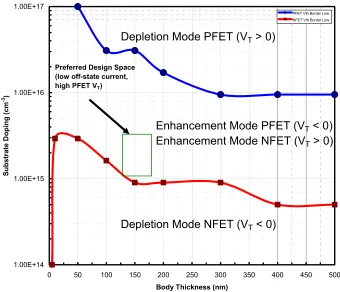
CMOS, is not without its compromise. Figure 10 shows the range of silicon film
thickness and doping at which both the NFET and PFET still have enhancement mode
threshold voltages (VTn > 0 and VTp < 0), assuming no fixed or trap charge. For most of
the devices considered in this work, a dopant concentration range between 1×1015 cm-3
and 3×1015 cm-3 was used as indicated by the boxed region in Figure 10. This favors a
higher magnitude PFET threshold voltage than the NFET. This dopant range allows room
for the NFET to be further adjusted with the addition of more dopant to increase the
magnitude of the threshold voltage without influencing the PFET. Compensating the
NFET device is more favorable because excess dopant would have lower impact on the
electron mobility than the hole mobility.
Figure 11 shows the dependence of the extracted VT of a simulated AMPFET with
varying NA at different values of XSi, assuming a gate metal workfunction of
molybdenum (ΦM = 4.53 eV), a gate oxide thickness of 50 nm, and neglecting interface
charge. The AMPFET VT is most sensitive to changes in XSi at higher doping
concentrations, where operation is depletion mode. At NA values below 1015 cm-3 the
threshold voltage becomes relatively constant, converging towards the
metal-semiconductor workfunction difference (ΦMS) in order to establish a flatband condition,
which can be considered analogous to the onset of inversion in the accumulation-mode
1.00E+14 1.00E+15 1.00E+16 1.00E+17
0 50 100 150 200 250 300 350 400 450 500 Body Thickness (nm)
S
u
bstr
ate
Doping
(c
m
-3)
PFET Vth Border Line NFET Vth Border Line
Enhancement Mode PFET (VT < 0) Enhancement Mode NFET (VT > 0)
Depletion Mode NFET (VT < 0) Depletion Mode PFET (VT > 0)
[image:44.612.151.491.174.466.2]Preferred Design Space (low off-state current, high PFET VT)
Figure 10. The delineation between enhancement and depletion mode threshold voltages for SiOG NFETs and PFETs. The region in the center of the plot indicated ranges of siliocon body thickness and substrate doping applicable for fabricating SiOG CMOS with enhancement mode threshold voltages on both Devices. The square indicates the preferred design space for CMOS utilizing a inversion mode NFET and an accumulation mode PFET. Working in this design space would increase the magnitude of the PFET threshold voltage and lower the NFET’s. This is such that compensation could be considered later in processing to help raise the threshold voltage with a minimal impact on mobility lowering.. (For both
-1.5 -1 -0.5 0 0.5 1 1.5
1.E+14 1.E+15 1.E+16 1.E+17
T
h
re
sho
ld V
o
lt
age
(V
)
Body Doping (cm-3)
1.4
133.1 13.5
Resistivity (Ωcm)
[image:45.612.156.502.76.375.2]0.2
Figure 11 Simulation of the effects of body doping concentration and silicon film thickness on the linearly extroplated threshold voltage of a thin-film accumulation-mode PFET on glass. The threshold voltage is that from a linear extrapolation on an IDS vs. VGS plot. A negative (positive) threshold voltage denotes an enhancement (depletion) mode biasing scheme. A 50 nm gate oxide and molybdenum workfunction of 4.53 eV were used.
An enhancement-mode VT by itself does not guarantee adequate subthreshold
characteristics and off-state leakage current. The 2D numerical simulation of minimum
current of an AMPFET transistor is show in Figure 12 with enhancement and depletion
mode regions indicated. For a given film thickness and dopant concentration, the
threshold voltage may appear to be enhancement mode, but the off-state characteristics
would suggest that it is not functioning well. Obviously at high doping and high thickness
the off-state leakage current should be relatively high; for thin thickness and low doping
Minimum Off-State Current for Thin-Film PFET on P-type Silicon Film
Gate Oxide: 500Å, Molybdenum Gate (ΦΜ = 4.53V), Linear Regime
1.00E-20 1.00E-19 1.00E-18 1.00E-17 1.00E-16 1.00E-15 1.00E-14 1.00E-13 1.00E-12 1.00E-11 1.00E-10 1.00E-09 1.00E-08 1.00E-07 1.00E-06 1.00E-05 1.00E-04
1.E+14 1.E+15 1.E+16 1.E+17
Body Doping (cm-3)
O ff-S ta te Cur re nt (A) 50 nm 100 nm 150 nm 200 nm 300 nm 400 nm 500 nm Silicon Thickness
[image:46.612.152.489.109.399.2]Enhancment Mode Depletion Mode
Figure 12. Simulation of the minimum off-state current of the thin-film PFET on glass. The dotted line
denotes whether the transistor is operating as an enhancement mode or a depletion mode device (i.e it
represents the current at the extracted threshold voltage). Even if a transistor has an enhancement mode
threshold voltage is still may not have adequate off-state characteristics. If the silicon film is too thick, or the body dopant concentration is too high, there will be a significant amount of leakage current. Current
values < 10-15 A are subject to numerical error from the simulation software.
Considering a very thin film or a very lightly doped film would be the best choice to
main low leakage current levels and an enhancement mode threshold voltage. In this
range, there is leeway to allow for slight variation in these factors without seeing a
significant increase in the leakage current.
A metric was developed to maintain specific off-state characteristics while adjusting
device design parameters. This metric is derived from the ratio of current at the threshold
voltage (IVT) and the current with the gate at zero-bias (Io); the logarithmic value of this
The number of decades required for adequate transistor performance is an engineering
decision and is chosen based on the device application. Figure 13 is plot of the design
metric Log(IVT/Io) vs. p-type dopant concentration for various silicon film thicknesses.
1 2 3 4 5 6 7 8
1E+15 1E+16
L
og(
IVT /Io
)
Dopant Concetration (cm-3)
Xsi = 200 nm Xsi = 180 nm Xsi = 150 nm Xsi = 120 nm Xsi = 100 nm
PFET
[image:47.612.156.487.162.491.2]NFET
Figure 13. Numerical modeling of design space for NFET and AMPFET transistors on SiOG under ideal
conditions; considering no interface charge or trap states. The off-state metric is Log(IVT/Io), described in
the text. Devices with a channel length of 2 µm and a gate oxide thickness of 50 nm were simulated using a molybdenum gate workfunction. Intersecting points of same film thickness represents symmetric operation of both the NFET and AMPFET transistors with threshold voltages of the same magnitude.
Figure 13 provides a comprehensive assessment of both the NFET and PFET off-state
performance achievable at different values of NA and XSi. A value of 6 for the off-state
metric would represent an excellent discrimination between on-state and off-state current.
values, however a compromise is required to provide equivalent off-state performance.
The intersecting points of matched XSi characteristics in Figure 13 define the
performance of NFETs and PFETs with the same body doping level. As shown in the
figure, the highest span of current drop is about 4.25 at XSi of 100 nm and NA of
6.7×1015 cm-3. Note that interface charge or trap states that may exist at either the top or
bottom silicon layer interface has not been considered. The presence of charge states can
have a significant influence on subthreshold behavior, yielding results which may be
interpreted as either better or worse than this ideal scenario.
While the explanation of ideal SiOG TFT behavior is easily discussed by parameters
which that can directly control, real devices are affected by non-idealities such as surface
finish and contamination. In Chapters 5 and 6, a discussion of SiOG TFT performance
will be conducted in the context of fabricated devices. The impact of non-ideal effects
C
HAPTER5
P
ROCESSR
EFINEMENTT
OWARDSI
MPROVEDD
EVICEP
ERFORMANCE5.1Introduction
In this chapter, a discussion of changes to substrate preparation and processing along
with their effects on device performance is given. Small refinements in the substrate
preparation before and during process can and do have a substantial impact on the final
elect