Version: Accepted Version
Article:
Bishop, Z.K., Foster, A. orcid.org/0000-0002-5817-0008, Royall, B. et al. (4 more authors)
(2018) Electro-mechanical control of an on-chip optical beam splitter containing an
embedded quantum emitter. Optics Letters, 43 (9). pp. 2142-2145. ISSN 0146-9592
https://doi.org/10.1364/OL.43.002142
[email protected]
https://eprints.whiterose.ac.uk/
Reuse
Items deposited in White Rose Research Online are protected by copyright, with all rights reserved unless
indicated otherwise. They may be downloaded and/or printed for private study, or other acts as permitted by
national copyright laws. The publisher or other rights holders may allow further reproduction and re-use of
the full text version. This is indicated by the licence information on the White Rose Research Online record
for the item.
Takedown
If you consider content in White Rose Research Online to be in breach of UK law, please notify us by
Electro-mechanical control of an on-chip optical beam
splitter containing an embedded quantum emitter
Z.K. B
ISHOP1,*, A.P. F
OSTER1, B. R
OYALL1, C. B
ENTHAM1, E. C
LARKE2, M.S. S
KOLNICK1,
ANDL.R. W
ILSON11Department of Physics and Astronomy, University of Sheffield, Sheffield S3 7RH, United Kingdom
2Department of Electronic and Electrical Engineering, University of Sheffield, Sheffield S1 3JD, United Kingdom *Corresponding author: [email protected]
Compiled March 26, 2018
We demonstrate electro-mechanical control of an on-chip GaAs optical beam splitter containing a quantum dot single photon source. The beam splitter consists of two nanobeam waveguides, which form a directional coupler. The splitting ratio of the directional coupler is controlled by varying the out-of-plane separation of the two waveguides using electromechanical actuation. We reversibly tune the beam splitter between an ini-tial state, with emission into both output arms, and a final state with photons emitted into a single output arm. The device represents a compact and scalable tun-ing approach for use in III-V semiconductor integrated quantum optical circuits. © 2018 Optical Society of America
OCIS codes: (130.4815) Optical switching devices; (230.4685) Optical microelectromechanical devices; (270.5585) Quantum information and pro-cessing.
http://dx.doi.org/10.1364/ao.XX.XXXXXX
Micro-opto-electro-mechanical systems (MOEMS) have been widely studied for a variety of applications in semiconductor integrated photonic circuits. The vast majority of work has been carried out in silicon where on-chip tuning of the optical properties of essential circuit components is possible by displac-ing them mechanically with the application of an electrostatic field. Lateral displacement has been used in phase modula-tors [1,2], resonance tuning of nanobeam photonic-crystal cav-ities (PhCCs) [3,4] and microtoroid resonators [5]. More com-plicated structures such as comb-drive actuators have also been developed to allow for larger displacements [6–10], attractive for optical switching applications [11–14]. Recently, scalable out-of-plane actuation methods have also been demonstrated at room temperature based on a cantilever geometry [15].
MOEMS based on III-V semiconductors are now emerging for applications in quantum information processing (QIP). Ini-tial work has focused on tuning of PhCC modes into resonance with quantum emitters in order to enhance their emission. In-plane [16] as well as double-membrane out-of-plane actuation methods have been reported [17–19]. Beam splitters, realized on chip using directional couplers (DCs), are another key com-ponent of integrated linear quantum optical circuits, with
post-fabrication control of their optical properties likely required for efficient QIP applications [20,21]. In this context, electro-mechanical tuning of DCs has so far only been considered theo-retically by Liu et al. [22], using a double-membrane actuation approach.
In this Letter we demonstrate the electro-mechanical control of an on-chip beam splitter operating at low temperature probed using single photon emission from an embedded InGaAs quan-tum dot (QD). The proposed device is compact, easy-to-fabricate and scalable [15] with large achievable out-of-plane displace-ments of over 400 nm. The device structure is versatile and can be adapted to fine tune other on-chip photonic elements. It represents a significant step towards reconfigurable integrated quantum optical circuits with embedded single photon sources. The operating principle of our device is shown schematically in Fig.1. The DC acts as an optical beam splitter for light enter-ing the input arm, due to evanescent light couplenter-ing between the two waveguides in the coupling region. The ratio of the output power in the through and drop arms of the DC is defined as the splitting ratio (SR). The SR depends on the dimensions of the waveguides, the wavelength of the transmitted light, and both in-plane,sin, and out-of-plane,sout, separations between
the waveguides. Here, we tune the parametersoutin order to
control the SR of the beam splitter.
To determine the theoretical change in the SR of the DC assout
is varied, 2D electromagnetic modeling was undertaken using MIT Photonic-Bands, a freely available eigenmode solver. The results for a range of wavelengths are shown in Figure1(c) for a DC consisting of 160 nm thick and 280 nm wide single (TE) mode waveguides, separated laterally bysin=40 nm in a 7µm long
coupling region (lc). It is clear that in a broadband QD emission
wavelength range of 880−980 nm, the DC can be tuned from an overcoupled state, when more light is coupled to the drop than the through arm, to a decoupled state, when all the light is trans-mitted to the through arm, assoutis increased to an achievable
Fig. 1.(a) Top- and (b) side- view schematic diagram of a nanobeam waveguide directional coupler. (c) Results of the modeling of a directional coupler consisting of 160 nm thick and 280 nm wide waveguides, separated laterally by 40 nm in a 7µm long coupling region. The contour plot shows how the
fraction of light evanescently coupled from one channel to the other depends on the wavelength of the transmitted light and the out-of-plane separation between the waveguides.
Experimentally, we control sout by attaching one of the
nanobeam waveguides of a DC to a mechanically compliant cantilever, which is actuated electro-mechanically to induce out-of-plane waveguide separation. Figure2(a) shows our proof-of-concept device, consisting of a GaAs nanobeam waveguide DC with one waveguide attached to the free end of a 35µm long
and 7.5µm wide cantilever, and the other fixed rigidly to the
bulk of the sample. Each arm is terminated with a Bragg output-coupler (OC) to enable out-of-plane collection of transmitted photons. The free end of the cantilever is supported on either side by a 300 nm wide sacrificial strut during sample fabrication and transport. The struts are removed before measurements commence using local laser ablation, releasing the cantilever.
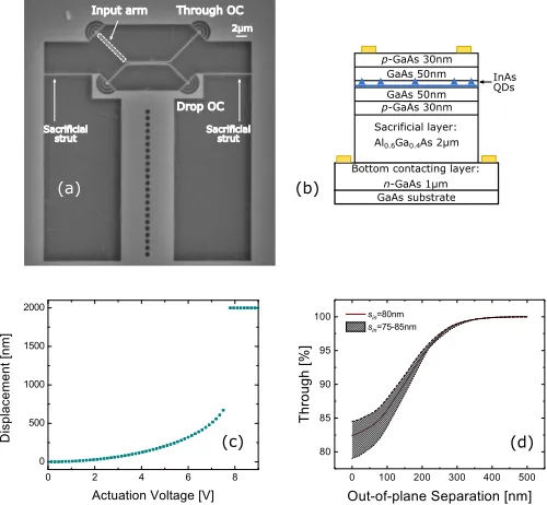
The device was fabricated on ap-i-p-i-ndiode, the schematic of which is presented in Fig.2(b). The DC and the cantilever were defined within the 160 nm thick topp-i-pGaAs membrane using electron-beam lithography followed by an inductively coupled plasma etch. The intrinsic region of this membrane con-tained InGaAs self-assembled QDs, used as embedded single photon sources to probe the optical response of the system. The n-GaAs substrate was electrically isolated from the membrane by a 2µm thick intrinsic Al0.6Ga0.4As layer, which was removed from underneath the device using an HF etch to create the sus-pended structure. The stresses that may occur in the structure due to surface tension when drying the device in air afterwards were minimized using a critical point drying technique. In this method the rinsing water was purged with liquid CO2and the sample was brought to the temperature and pressure critical for CO2, allowing to dry the device without surface tension present. Ni:Au contacts were made to the topp- and the bottomn-GaAs layers in order to allow for electro-mechanical control of the can-tilever. The row of holes in the center of the device [see Fig.2(a)] allowed for faster under-etching of the cantilever.
[image:3.612.315.565.47.278.2]Applying an actuation voltage,Vact, between the cantilever
Fig. 2.(a) Top-view scanning electron microscope image of a
typical device. The sacrificial struts are removed at low tem-perature before the opto-electro-mechanical measurements. (b) Schematic diagram of the wafer structure. The position of contacts is marked by gold rectangles. (c) Calculated displace-ment of the free end of the 35µm long and 7.5µm wide
can-tilever as actuation voltage is increased. (d) Modeled overall percentage of light transmitted to the through output-coupler with increasing out-of-plane waveguide separation for the experimental device withsin=80±5 nm.
and the substrate results in a capacitive force, which causes the cantilever to deflect towards the substrate. This introduces a vertical out-of-plane separation between the two arms of the DC. Figure2(c) shows the displacement of the free end of the cantilever as Vact is increased, calculated using an analytical
model which determines the displacement for a givenVactby
minimizing the total energy of the system (comprising strain and electrostatic energies). The model assumes that the cantilever’s vertical displacement is a quadratic function of position along its length [23]. The theoretical maximum controllable displace-ment of the cantilever is 1/3 of the initial distance between the cantilever and the substrate,s0[24]. Once this displacement is reached at the so-called pull-in voltage,Vpull, the capacitive
force becomes greater than the restoring force and the free end of the cantilever collapses onto the substrate. This introduces sur-face adhesion forces between the cantilever and the substrate. If these forces are smaller than the restoring force of the cantilever, the cantilever will be able to lift back up from the substrate at Vact<Vpullresulting in a hysteresis behavior [25,26]. For our
systemVpullis calculated to occur at 7.5 V, when the
discontinu-ity in the filled squares curve is observed between the displace-ment of 667 nm and 2000 nm (corresponding tospull=s0/3 and s0).
Our proof-of-concept device had a waveguide width of 280 nm andsin=80±5 nm. The latter is∼40 nm larger than the
wave-Fig. 3. Filtered PL collection map of the device with an over-laid device contour with (a)Vact=0 V, and (b)Vact=12.5 V.
length chosen is 910 nm as this is the emission wavelength of the single QD studied experimentally. The initial SR is∼83:17, and can be increased to 100:0 forsout>300 nm. The model is
in good qualitative agreement with our experimental results, as we show below.
The electro-mechanical behavior of the cantilever was studied experimentally using white light illumination of the sample in a cryostat at 4.2 K using a confocal microscope system and an infrared camera. AsVactwas increased the free end of the
cantilever was observed to collapse onto the substrate at 13 V, and then lift back up asVactwas decreased to 4 V, allowing for
multiple measurements to be performed. This was possible due to two factors. Firstly, larges0 means a large restoring force of the cantilever, which counters the surface adhesion forces present after the collapse. Secondly, only a small portion of the free end of the cantilever is actually in contact with the substrate, minimizing the action of these forces. The largerVact, compared
to the modeling, required for the actuation of our cantilever could simply be related to the resistance of the contacts, which is not taken into account in the modeling.
The device was studied optically using
micro-photoluminescence (µ-PL) spectroscopy with spatially
resolved excitation and collection in an exchange gas cryostat at 4.2 K using a confocal microscope system. For the measure-ments of the SR we selected a bright and spectrally isolated QD embedded within the input arm of the fixed waveguide of the DC, emitting at 910.6 nm. The QD was excited from above via the wetting layer using a Ti:Sapphire CW laser emitting at 840 nm. Figure3shows twoµ-PL maps, with the device contour
overlaid, obtained by raster scanning the collection across the device while spectrally filtering at the QD wavelength. Figure3(a) was obtained from the device withVact =0 V and
emission can be seen from both the through and drop OCs. The
µ-PL map in Fig.3(b) was acquired for the device operated with
Vact=12.5 V, and emission from the drop OC is observed to be
heavily suppressed, while that from the through OC increases as expected.
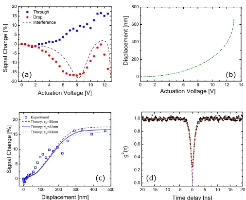
To characterize the device at increasing out-of-plane waveg-uide separation, the routed QD emission was measured simul-taneously from the through (fixed) and the drop (moving) OCs using two independent collection paths asVactwas increased.
The SR for the device atVact =0 V was measured to be 80:20.
The absolute percent change to the measured signal is shown in Fig.4(a) for the through and drop OCs separately. The sig-nal is normalized to the total sigsig-nal collected from both OCs at Vact =0 V. The change in the QD emission collected from the
through OC increases monotonically until it saturates at 17% for Vact>11 V. The signal at the drop OC decreases initially as
ex-pected, but then recovers and peaks at aboutVact=11.5 V before
[image:4.612.318.571.41.247.2]decreasing again. This is caused by the downward movement of the drop OC asVactis applied, which results in changes to the
Fig. 4.(a) Measured changes to the QD signal collected from
the through and drop OCs independently, as actuation volt-age is increased. The signal is normalized to the total signal recorded from both OCs atVact =0 V. The peak in the signal
from the drop OC at aboutVact = 11 V is due to changing
optical interference from the moving OC during cantilever actuation (modeled using the transfer-matrix method). (b) Cantilever displacement as a function of actuation voltage for the measured system, found using Eq. (2) withX=2650. (c) Experimental results (empty squares) for the through OC from graph (a) as a function of displacement converted from actua-tion voltage using the relaactua-tionship in Fig.4(b). The other three lines are theoretical curves forsinof 80, 82, and 84 nm
normal-ized to the initial signal at zero displacement. (d) Normalnormal-ized second-order correlation function obtained by exciting the QD from above and collecting the spectrally filtered PL signal from the input OC. The orange continuous line is a fit to the experimental data (black points), while the dashed purple line represents a fit that takes into account the time response of the measurement system.
optical interference of signal emitted from the OC and that re-flected from the substrate as well as collection efficiency changes. While the optical interference effect can be modeled using the transfer-matrix method, which explains the peaks and troughs in the signal measured from the drop OC (see Fig.4(a)), the collec-tion efficiency changes are more difficult to estimate. In addicollec-tion, without performing fully coupled opto-electro-mechanical sim-ulations it is not possible to deconvolve these effects acting on the drop OC from the evanescent coupling that is of interest. Hence, we proceed to determine the controlled changes to the splitting ratio based on the through OC only. A small QD Stark-shift of 0.15 nm was also observed asVactwas increased from
0 V to 12.5 V, due to the increasing electric field between the toppdoped layer of the membrane and thendoped substrate.
Contacting the lower pdoped layer of the GaAs membrane
would eliminate the Stark shift, and would enable simultaneous electro-mechanical actuation and QD Stark tuning [19].
In order to directly compare the controlled optical properties of the DC with the modeling [shown in Fig.2(d)],Vactwas
[image:4.612.46.297.44.129.2]substrate (here 2000 nm),sout is the displacement of the
can-tilever,ǫ0is the permittivity of free space,Ais the surface area of the cantilever, andk is a fitting parameter corresponding to an average stiffness of the cantilever. We thus derived the relationship betweenVactand the displacement as follows:
Vact=
(s0−sout)√sout
X , (2)
whereX=√ǫ0A/2k nm3/2V-2.
The parameterXfor our measured device was found using
Vpull=13 V (the observed pull-in voltage) and the theoretical maximum displacement ofspull =667 nm. Equation (2) with
X=2650 was then used to convertVactto cantilever
displace-ment and the resulting curve is shown in Fig.4(b).
This conversion allows us to directly compare the experimen-tally determined variation in the QD emission routed to the through OC with that calculated using the eigenmode solver [the results of which are presented in Fig.2(d)]. The experimen-tal curve is in the best agreement with the theoretical curve for sin = 82 nm, presented in Fig.4(c) as a function of cantilever
displacement. The two curves demonstrate monotonic increase of the QD signal until saturation at 17 % for displacements of over 300 nm. The achieved displacement of the cantilever was found to be over 400 nm before the pull-in occurs.
We verified the single-photon nature of the emission from this QD by performing an on-chip Hanbury Brown and Twiss experiment, which consists of cross-correlating the photons at the QD wavelength collected by two separate paths from the input OC. The results are shown in Fig.4(d), with normalized g(2)(0) =0.25±0.02. By deconvolving the experimental data
with the temporal response of our detection system (Gaussian, full-width-at-half-maximum of 874±4 ps) we obtaing(2)(0) =
0±0.01, which indicates that the source is strongly antibunched. The electro-mechanical system presented here can not only be used to control the SR of an on-chip beam splitter but also to fine tune other integrated photonic devices. Greater versatil-ity and scalabilversatil-ity of the system can be achieved through some improvements to the sample design [15], which could enable it to operate as an optical router with an expected switching rate of the order of 0.5 MHz. Further optimization of the di-mensions of the DC can overcome the difficulties in achieving small enough in-plane separations needed in the reported de-vice for larger tuning range covering the commonly required 50:50 splitting. Increasing the coupling length of the DC or decreasing the cross section of the waveguides are examples of promising approaches worth investigating. Operating the beam splitter at longer telecoms wavelengths is another solution to achieving 50:50 splitting with larger and easier to achieve in-plane waveguide separations. Fabricating the structure on ap-i-n-i-ndiode and depositing a third contact on the middle n-layer would enable tuning of the QD emission wavelength using the quantum-confined Stark effect [27] at the same time as controlling the beam splitter electro-mechanically. The op-erating actuation voltage could also be decreased by using a thinner AlGaAs sacrificial layer, reducing the initial distance between the two electrodes. Alternatively, if the device footprint is of importance, the AlGaAs thickness could be decreased in
ments of over 400 nm. An embedded quantum emitter was used to probe the optical response of the system. The splitting ratio of our on-chip optical beam splitter was tuned from an initial∼80:20 atVact=0 V (zero displacement) up to∼100:0
at Vact = 11 V (300 nm displacement). The proposed device
operates as a fine tuning element and paves the way toward increased control of on-chip single photon devices using com-pact, easy-to-fabricate and scalable structures for use in III-V semiconductor integrated quantum optical circuits.
This work was funded by EPSRC Grants No. EP/J007544/1 and EP/N031776/1. The data from this study is available at 10.15131/shef.data.6022892.
REFERENCES
1. K. Van Acoleyen, J. Roels, P. Mechet, T. Claes, D. Van Thourhout, and R. Baers, IEEE Photon. J.4, 779 (2012).
2. M. Winger, T. D. Blasius, T. P. Alegre, A. H. Safavi-Naeini, S. Meenehan, J. Cohen, S. Stobbe, and O. Painter, Opt. Express19, 24905 (2011). 3. P. B. Deotare, M. W. McCutcheon, I. W. Frank, M. Khan, and M. Lonˇcar,
Appl. Phys. Lett.95, 031102 (2009).
4. I. W. Frank, P. B. Deotare, M. W. McCutcheon, and M. Lonˇcar, Opt. Express18, 8705 (2010).
5. C. G. Baker, C. Bekker, D. L. McAuslan, E. Sheridan, and W. P. Bowen, Opt. Express14, 20400 (2016).
6. R. Legtenberg, A. W. Groeneveld, and M. Elwenspoek, J. Micromech. Microeng.6, 320 (1996).
7. G. Zhou and P. Dowd, J. Micromech. Microeng.13, 178 (2003). 8. X. Chew, G. Zhou, F. S. Chau, J. Deng, X. Tang, and Y. C. Loke, Opt.
Lett.35, 2517 (2010).
9. X. Chew, G. Zhou, H. Yu, F. S. Chau, J. Deng, L. Y. C., and X. Tang, Opt. Express18, 22232 (2010).
10. P. Shi, G. Zhou, J. Deng, F. Tian, and F. S. Chau, Sci. Rep.5, 14379 (2015).
11. E. Bulgan, Y. Kanamori, and K. Hane, Appl. Phys. Lett.92, 101110 (2008).
12. Y. Akihama, Y. Kanamori, and K. Hane, Opt. Express19, 23658 (2011). 13. Y. Akihama and K. Hane, Light Sci. Appl.1, e16 (2012).
14. Y. Munemasa and K. Hane, Jpn. J. Appl. Phys.52, 06GL15 (2013). 15. S. Han, T. J. Seok, N. Quack, B. W. Yoo, and M. C. Wu, Optica2, 370
(2015).
16. R. Ohta, Y. Ota, H. Takagi, N. Kumagai, K. Tanabe, S. Ishida, S. Iwamoto, and Y. Arakawa, Jpn. J. Appl. Phys.52, 04CG01 (2013). 17. L. Midolo, P. J. van Veldhoven, M. A. Dündar, R. Nötzel, and A. Fiore,
Appl. Phys. Lett.98, 211120 (2011).
18. L. Midolo, S. N. Yoon, F. Pagliano, T. Xia, F. W. M. van Otten, M. Lermer, S. Höfling, and A. Fiore, Opt. Express20, 19255 (2012).
19. M. Petruzzella, T. Xia, F. Pagliano, S. Birindelli, L. Midolo, Z. Zobenica, L. H. Li, E. H. Linfield, and A. Fiore, Appl. Phys. Lett.107(2015). 20. E. Knill, R. Laflamme, and G. J. Milburn, Nature409, 46 (2001). 21. H. J. Kimble, Nature453, 1023 (2008).
22. T. Liu, F. Pagliano, and A. Fiore, Opt. Express25, 10166 (2017). 23. S. Tsuchitani and R. Kaneko, T. IEE Japan118, 6 (1998). 24. L. Midolo and A. Fiore, IEEE J. Quant. Electron.50, 404 (2014). 25. J. O. Lee, Y.-H. Song, M.-W. Kim, M.-H. Kang, J.-S. Oh, H.-H. Yang,
and J. B. Yoon, Nat. Nanotechnol.8, 36 (2013).
26. O. Buchnev, N. Podoliak, T. Frank, M. Kaczmarek, L. Jiang, and V. A. Fedotov, ACS Nano10, 11519 (2016).
1. K. Van Acoleyen, J. Roels, P. Mechet, T. Claes, D. Van Thourhout, and R. Baers, “Ultracompact phase modulator based on a cascade of NEMS-operated slot waveguides fabricated in silicon-on-insulator,” IEEE Photon. J.4, 779–788 (2012).
2. M. Winger, T. D. Blasius, T. P. Alegre, A. H. Safavi-Naeini, S. Meene-han, J. Cohen, S. Stobbe, and O. Painter, “A chip-scale integrated cavity-electro-optomechanics platform,” Opt. Express19, 24905–24921 (2011).
3. P. B. Deotare, M. W. McCutcheon, I. W. Frank, M. Khan, and M. Lonˇcar, “Coupled photonic crystal nanobeam cavities,” Appl. Phys. Lett.95, 031102 (2009).
4. I. W. Frank, P. B. Deotare, M. W. McCutcheon, and M. Lonˇcar, “Pro-grammable photonic crystal nanobeam cavities,” Opt. Express18, 8705–8712 (2010).
5. C. G. Baker, C. Bekker, D. L. McAuslan, E. Sheridan, and W. P. Bowen, “High bandwidth on-chip capacitive tuning of microtoroid resonators,” Opt. Express14, 20400–20412 (2016).
6. R. Legtenberg, A. W. Groeneveld, and M. Elwenspoek, “Comb-drive actuators for large displacements,” J. Micromech. Microeng.6, 320– 329 (1996).
7. G. Zhou and P. Dowd, “Tilted folded-beam suspension for extending the stable travel range of comb-drive actuators,” J. Micromech. Microeng.
13, 178–183 (2003).
8. X. Chew, G. Zhou, F. S. Chau, J. Deng, X. Tang, and Y. C. Loke, “Dynamic tuning of an optical resonator through mems-driven coupled photonic crystal nanocavities,” Opt. Lett.35, 2517–2519 (2010). 9. X. Chew, G. Zhou, H. Yu, F. S. Chau, J. Deng, L. Y. C., and X. Tang, “An
in-plane nano-mechanics approach to achieve reversible resonance control of photonic crystal nanocavities,” Opt. Express18, 22232– 22244 (2010).
10. P. Shi, G. Zhou, J. Deng, F. Tian, and F. S. Chau, “Tuning all-optical ana-log to electromagnetically induced transparency in nanobeam cavities using electromechanical system,” Sci. Rep.5, 14379 (2015). 11. E. Bulgan, Y. Kanamori, and K. Hane, “Submicron silicon waveguide
optical switch driven by microelectromechanical actuator,” Appl. Phys. Lett.92, 101110 (2008).
12. Y. Akihama, Y. Kanamori, and K. Hane, “Ultra-small silicon waveg-uide coupler switch using gap-variable mechanism,” Opt. Express19, 23658–23663 (2011).
13. Y. Akihama and K. Hane, “Single and multiple optical switches that use freestanding silicon nanowire waveguide couplers,” Light Sci. Appl.1, e16 (2012).
14. Y. Munemasa and K. Hane, “A compact 1x3 silicon photonic waveguide switch based on precise investigation of coupling characteristics of variable-gap coupler,” Jpn. J. Appl. Phys.52, 06GL15 (2013). 15. S. Han, T. J. Seok, N. Quack, B. W. Yoo, and M. C. Wu, “Design and
optical properties of electromechanical double-membrance photonic crystal cavities,” Optica2, 370–375 (2015).
16. R. Ohta, Y. Ota, H. Takagi, N. Kumagai, K. Tanabe, S. Ishida, S. Iwamoto, and Y. Arakawa, “Electro-mechanicalQfactor control of photonic crystal nanobeam cavity,” Jpn. J. Appl. Phys.52, 04CG01 (2013).
17. L. Midolo, P. J. van Veldhoven, M. A. Dündar, R. Nötzel, and A. Fiore, “Electromechanical wavelength tuning of double-membrane photonic crystal cavities,” Appl. Phys. Lett.98, 211120 (2011).
18. L. Midolo, S. N. Yoon, F. Pagliano, T. Xia, F. W. M. van Otten, M. Lermer, S. Höfling, and A. Fiore, “Electromechanical tuning of vertically-coupled photonic crystal nanobeams,” Opt. Express20, 19255–19263 (2012). 19. M. Petruzzella, T. Xia, F. Pagliano, S. Birindelli, L. Midolo, Z. Zobenica, L. H. Li, E. H. Linfield, and A. Fiore, “Fully tuneable, purcell-enhanced solid-state quantum emitters,” Appl. Phys. Lett.107(2015).
20. E. Knill, R. Laflamme, and G. J. Milburn, “A scheme for efficient quan-tum computation with linear optics,” Nature409, 46–52 (2001). 21. H. J. Kimble, “The quantum internet,” Nature453, 1023–1030 (2008). 22. T. Liu, F. Pagliano, and A. Fiore, “Nano-opto-electro-mechanical switch based on a four-waveguide directional coupler,” Opt. Express25, 10166–10176 (2017).
under electrostatic force,” T. IEE Japan118, 6–13 (1998).
24. L. Midolo and A. Fiore, “Design and optical properties of electrome-chanical double-membrane photonic crystal cavities,” IEEE J. Quant. Electron.50, 404–4014 (2014).
25. J. O. Lee, Y.-H. Song, M.-W. Kim, M.-H. Kang, J.-S. Oh, H.-H. Yang, and J. B. Yoon, “A sub-1-volt nanoelectromechanical switching device,” Nat. Nanotechnol.8, 36–40 (2013).
26. O. Buchnev, N. Podoliak, T. Frank, M. Kaczmarek, L. Jiang, and V. A. Fedotov, “Controlling stiction in nano-electro-mechanical systems using liquid crystals,” ACS Nano10, 11519–11524 (2016).