Rochester Institute of Technology
RIT Scholar Works
Theses Thesis/Dissertation Collections
5-18-2011
Development of a deep submicron fabrication
process for tunneling field effect transistors
Michael Barth
Follow this and additional works at:http://scholarworks.rit.edu/theses
This Thesis is brought to you for free and open access by the Thesis/Dissertation Collections at RIT Scholar Works. It has been accepted for inclusion in Theses by an authorized administrator of RIT Scholar Works. For more information, please contactritscholarworks@rit.edu.
Recommended Citation
Development of a Deep Submicron Fabrication Process for
Tunneling Field Effect Transistors
By
Michael J. Barth
A Thesis Submitted in Partial Fulfillment
of the Requirements for the Degree of Master of Science
in Microelectronic Engineering Approved by:
Professor: ___________________________________________ Dr. Sean L. Rommel (Thesis Advisor)
Professor: ___________________________________________ Dr. Santosh K. Kurinec (Thesis Committee Member)
Professor: ___________________________________________ Dr. James E. Moon (Thesis Committee Member)
Professor: ___________________________________________ Dr. Robert Pearson (Thesis Committee Member)
Approved on: May 18, 2011
DEPARTMENT OF ELECTRICAL & MICROELECTRONIC ENGINEERING COLLEGE OF ENGINEERING
Development of a Deep Submicron Fabrication Process for
Tunneling Field Effect Transistors
By
Michael J. Barth
I, Michael J. Barth, hereby grant permission to the Wallace Memorial Library of the Rochester Institute of Technology to reproduce this document in whole or in part that any reproduction will not be for commercial use or profit.
_________________________________ ________________________
I dedicate this thesis to my family: my mother Adrienne, my
father Bernard, my sister Megan, and my Grandmother Victoria.
Acknowledgements
I would like to thank my advisor Dr. Rommel for his support and guidance over
the past three years. Your encouragement and insistence on student involvement and
collaboration with academic and industrial research has open many doors. I would also
like to thank Dr. Moon, Dr. Pearson and Dr. Kurinec, my thesis committee members for
their assistance and continued support.
I would like to acknowledge my fellow graduate students in the Microelectronic
Engineering program at RIT. I would especially like to thank David Pawlik and Paul
Thomas. Both were always there to listen to my ideas, offer suggestions and answer any
questions. Their help with electron beam lithography was invaluable. Furthermore I
would like to thank Marie Rohrbaugh for her help with the initial development of the BCB
via etch process.
This work would not have been possible without InGaAs samples to process. For
growing the InGaAs samples used throughout this work I would like to thank Dr. Dan
Ritter from the Technion, Israel Institute of Technology. For their support with ALD
deposition I would also like to thank Dr. Suman Datta from The Pennsylvania State
University and Dr. Wei-Yip Loh from Sematech.
I would like to thank the entire staff of the RIT Semiconductor and Microsystems
Fabrication Laboratory for their continuous support for the past few years. I would like
specifically thank Scott Blondell for six years ago hiring an inexperienced college
freshman to work in the lab. That first opportunity to work on semiconductor fabrication
equipment was invaluable. The knowledge and experience that I gained led to many more
of their help with the Perkin-Elmer 4400 and Perkin-Elmer 2400 sputtering systems.
Additionally I would like to Dave Yackoff, Bruce Tolleson, Sean O’Brien for their
Abstract
The requirements placed upon next-generation devices include high on-state
current, low power supply voltages, and low subthreshold swing. Tunneling Field Effect
Transistors (TFETs) have been of recent interest because they have the potential to fulfill
these requirements. The TFET is a gated tunnel junction. The TFET operates by
modulating the probability of band-to-band tunneling between the source and the channel
of the device. When the tunnel transistor is off, there is a potential barrier between the
source and the channel. The width of this potential barrier is large enough to prevent
electrons tunneling from the valence to conduction bands, the result of which is a lower
leakage current and improved power efficiency. The potential barrier narrows as bias is
applied to the gate. When the applied gate voltage exceeds the threshold voltage this
potential barrier becomes thin enough to allow for tunneling from the valence band to the
conduction band. The tunneling mechanism allows the device to have a high on-state
current and low subthreshold swing at low power supplies.
To date the majority of the work involving TFETs has been simulation-based.
Unfortunately the models used in these simulations are deficient. The models require
physical data for proper calibration [1]. The few experimental demonstrations of TFETs
have not yielded a body of empirical data sufficient for calibration. This work intends to
help provide that body of experimental data on gated and non-gated tunneling junctions in
Table of Contents
Abstract vi
Table of Contents vii
List of Figures ix
List of Tables x
List of Symbols xi
List of Acronyms xii
Chapter 1: Introduction and Motivation 1
Chapter 2: Background 3
(2.1) TFET Device Physics and Simulation 3
(2.2) Modeling TFET Behavior 13
(2.3) Esaki Diode 17
Chapter 3: Process Details 20
(3.1) Mesa-First Process Flow 21
(3.1.1) Surface Preparation 21
(3.1.2) Mesa Definition Lithography 22
(3.1.3) Mesa Etch 23
(3.1.4) MaN 2401 Resist Strip 24
(3.1.5) Gate Stack Deposition 26
(3.1.6) Benzocyclobutene (BCB) Deposition 27
(3.1.7) Benzocyclobutene (BCB) Etch Back 31
(3.1.8) Benzocyclobutene (BCB) Via Etch Lithography 32
(3.1.9) Benzocyclobutene (BCB) Via Etch 34
(3.1.10) Contact Metal Lithography and Deposition 35
(3.2) Metal-First Esaki Diode Process Flow 37
(3.3) Mesa-First TFET Layout 39
Chapter 4: Process Module Development 42
(4.1) Electron Beam Lithography 43
(4.2) BCB Deposition and Cure 51
(4.3) BCB Plasma Etching – Overburden Etch and Via Etch 53
(4.4) TaN Gating Development 57
Chapter 5: Results and Analysis 61
(5.1) RT-1 62
(5.1.1) RT-1 Process History 63
(5.1.1) RT-1 Electrical Results 65
(5.2) DRT Series TFETs 68
(5.2.1) DRT-1 Processing Summary and Electrical Results 69
(5.3) Modeling of Tunneling Currents 70
Chapter 6: Conclusions and Future Work 78
(6.1) Conclusions 78
(6.2) Future Work 80
List of Figures
Figure 2-1: TFET shown operating in p-channel mode 3
Figure 2-2: Simulated band diagram for a 100 nm n-channel silicon TFET 4
Figure 2-3: Band Diagram Tunneling Probability 5
Figure 2-4: Simulated band diagram for a 100nm n-channel silicon TFET 9
Figure 2-5: Simulated Results for Double Gate n-type Si TFET 11
Figure 2-6: Channel Doped Surface Tunnel Transistor (CD-STT ) Electrical Performance and Structure 14
Figure 2-7: TFET Family of curves Mookerjea, et al 15
Figure 2-8: Cross-sectional SEM image of the fabricated TFET 16
Figure 2-9: Transfer curve of the fabricated TFET 16
Figure 2-10: Esaki Diode Regions of Operation 19
Figure 3-1: First Level Lithography – Mesa Definition 23
Figure 3-2: Mesa Etch 24
Figure 3-4: MaN 2401 Resist Strip 25
Figure 3-4: Contaminated MaN 2401 - After 2 minutes O2 plasma 25
Figure 3-5: Gate Process Flows 27
Figure 3-6: BCB Deposition 29
Figure 3-7: BCB Etch Back 32
Figure 3-8: Level 3 Lithography- Via Etch 34
Figure 3-9: TFET Test Structure Die Level Layout 35
Figure 3-10: Final Cross Section 37
Figure 3-11: Metal-first Esaki Diode Process 38
Figure 3-12: Individual TFET Layout 40
Figure 3-13: TFET Test Structure Die Layout 41
Figure 4-1: Electron Beam Lithography Process 44
Figure 4-2: Comparison of PMMA LOR5A Coated III-V Mesa Alignment Mark Capture Between SEM and NPGS 46
Figure 4-3:
Comparison of PMMA LOR5A Coated Au and III-V Mesa Alignment Marks As Detected By NPGS Utilizing the Secondary Electron Detector
48
Figure 4-4: Comparison of NPGS III-V Mesa Alignment Marks Recognition, Secondary Electron Detector versus Backscattered Electron Detector 49
Figure 4- 5: Misaligned Top Contact Shorting to the Gate 50
Figure 4-6: The extent of BCB cure as a Function of Temperature and Time 53
Figure 4-7: BCB O2: SF6 (4:1) Plasma Etch 54
Figure 4-8: BCB O2: SF6 (4:1) Plasma Etch RF Power Versus Average Etch Rate 55
Figure 4-9: BCB Via Etch Rate 56
Figure 4-10: TaN Composition, Resistivity, and Sputter Rate as Function of Gas
Mixture 58
Figure 4-11: PE4400 TaN Deposition Rate at 400 W 59
Figure 5-1: Layer Structure RT-1 62
Figure 5-3: Fabricated TFET Side Profile Micrograph 64
Figure 5-4: TFET Top Down Profile Micrograph 65
Figure 5-5: Esaki Diode Comparison 66
Figure 5-6: RT-1 Gated Mesa IV Results 67
Figure 5-7: Layer Structure DRT 68
Figure 5-8: DRT-1 Metal-first Tunnel Diode IV Curve – Measurements Taken Following Mesa Etch 69
Figure 5-9: DRT-1 Metal-first Esaki Diode IV Curve – Measurements Taken Following Level 2 Metal 70
Figure 5-10: Current Density Versus Voltage - 150 nm Radius Metal-first Esaki
Diodes 72
Figure 5-11: Ratio of Zener Current and Forward Tunneling Current Versus Voltage y=AeBx A=0.94 B=7.2 73 Figure 5-12: Zener Empirical Model A=0.94 B=7.2 Vp=0.165 V Jp=183kA/cm2 74
Figure 5-13: Zener Empirical Model Function of Temperature 75
Figure 5-14: Fitting Constants as a Function of Temperature 75
List of Tables
Table 3-1: Level 1 Electron Beam Lithography Job Parameters 23
Table 3-2: MaN 2401 Strip Etch Recipe - LAM 490 AutoEtch 24
Table 3-3: Gate Level EBL LOR5A/PMMA Resist Coat Recipe 28
Table 3-4: Gate Level Electron Beam Lithography Job Parameters 28
Table 3-5: PE4400 TaN Sputter Deposition Recipe 29
Table 3-6: BCB Spin Coat Recipe 30
Table 3-7: BCB Etch Back Lam 490 AutoEtch Recipe 31
Table 3-8: BCB Via Etch LOR5A/PMMA Resist Coat Recipe 33
Table 3-9: Level 3 Electron Beam Lithography Job Parameters 33
Table 3-10: Contact Metal Lithography LOR5A/PMMA Resist Coat Recipe 35
Table 3-11: Level 4 Electron Beam Lithography Job Parameters 36
Table 3-12: Metal-first Process Details 39
List of Symbols
D Overlap Integral
ħ Planck’s Constant
ξ Electric Field
Eg Band Gap
m* Effective Mass
k Relative Permittivity
Vp Peak Voltage
Vv Valley Voltage
Jp Peak Current Density
List of Acronyms
TFET Tunneling Field Effect Transistor
MOSFET Metal Oxide Semiconductor Field Effect Transistor
PVCR Peak to Valley Current Ratio
EBL Electron Beam Lithography
ALD Atomic Layer Deposition
PE4400 Perkin Elmer 4400 Sputtering System
TiN Titanium Nitride
Chapter 1
Introduction
The desire for improved performance drives the search for next-generation
devices. While in the past this improved performance was quantified in terms of speed,
the new benchmark is performance with high efficiency. Causing this shift is the rise of
consumer demand for ultra-mobile devices and the push for efficient “green” technology.
The scaling of the power supplies for TFETs can be greater than that of Metal Oxide
Semiconductor Field-Effect Transistors (MOSFETs). TFETs require less power to operate
and thus are more efficient.
A high-order approximation of a TFET would be a gated Esaki tunnel diode. Esaki
diodes have a very abrupt and degenerately doped pn or p-i-n junction. This abrupt junction causes the conduction bands of the two highly doped regions to overlap. This
overlap allows for tunneling between the two regions when a small bias is applied. A
reverse bias on the Esaki diode results in Zener tunneling, while a forward bias results in a
tunneling component where the current increases with forward bias. TFETs are typically
operated in the Zener regime. The addition of a gate along the junction allows for control
of the conduction band overlap. With a small bias applied to the gate the conduction bands
will shift, allowing the gate to control the probability of tunneling.
Theoretically this gate control should allow for a device with a high on current,
low leakage current and a sub 60-mV/dec subthreshold slope. TFETs demonstrating all of
these properties have only been in realized in simulation. These simulated TFETs utilize
complex quantum and band-to-band tunneling models with discrete meshing to predict
low leakage currents and sub-60 mV/dec subthreshold slope [2]. Non-gated tunnel diodes
have shown tunnel junctions with high on currents of 975 kA/cm2 [3]. The models
themselves have also been reported to underestimate the current density of devices by up
to two orders of magnitude [1]. The disparity between simulation and experimental results
and the admitted errors with the models necessitate more experimental research on
tunneling junction, gated tunneling junctions, and TFETs.
This work introduces a mesa-first process for fabricating TFETs. The process
utilizes electron beam lithography to define a series of mesas in a p-i-n junction. A high-k
dielectric and a refractory metal are used to gate the sidewall of an individual mesa. This
process utilizes a spin-on dielectric to isolate the individual devices and enable a second
level contact. The dielectric layer and second level contact enables the fabrication of deep
submicron devices while allowing for large contact pads. Deep submicron scaling is
essential to studying tunneling devices as it allows for the perimeter to be a greater
Chapter 2
Background
2.1. TFET Device Physics and Simulation:
A TFET like the device shown in Figure 2-1 is a gated p-i-n diode. This TFET is a vertical structure with a polysilicon gate along the junction and sidewall of the device.
Top and bottom contacts are used to contact the n+ and p+ regions. The n+ and p+
regions can act as either the source or drain depending on bias conditions.
Figure 2-1: TFET shown operating in p-channel mode [4]
Applying a reverse bias to the gate of the TFET in Figure 2-1 creates a hole
channel in the insulator region (i-zone) leading to a tunnel junction at the n+ Si source. With reverse bias applied to the gate, the device is in the p-channel operation mode. Conversely applying a forward bias on the gate causes an electron channel to be induced
source. In both operating regimes the channel length is determined by the thickness of the
insulating region.
Figure 2-2: Simulated band diagram for a 100 nm n-channel silicon TFET [5]
As seen in Figure 2-2, when the applied gate voltage VGS is zero the separation between the conduction band in the insulating region and the valence band in the p+
region results in a very low probability that tunneling will occur. Thus the device is
considered to be off as no current will flow. As voltage applied to the gate is increased the
separation between the conduction and valence band narrows. Applying a voltage on the
gate of VGS =1.5 V lowers the barrier height thus increasing the probability of tunneling to occur. With a high probability of tunneling, the transistor is on.
Modeling the behavior of the TFET begins with Kane’s model for band-to-band
tunneling as seen in Eq 2-1 [6].
(2-1)
J = q2!
36"!2
2m*
Eg #D#exp $
" m*E g 3/ 2
2 2!!
This model is a function of the electric field ξ, the bandgap across the tunnel
junction Eg, Planck’s constant ħ and the effective carrier mass m*. The tunneling current effective mass is often assumed to be the conduction band effective mass. The D term in the expression for tunneling current refers to an overlap integral.
Figure 2-3: Band Diagram Tunneling Probability [6]
The band-to-band tunneling model developed by Kane assumes a triangular barrier
similar to the one shown in Figure 2-3 above. The model further assumes direct
tunneling, tunneling in which momentum is conserved. The overlap integral D shown in Eq. 2-2 [7] describes how the bands overlap as the electric field is varied.
(2-2)
D=
"
(
FC( )
E !FV( )
E)
1!exp !ESE # $%
& '( #
$
The overlap integral is dependent on Fc and Fv as well as two terms Es and Ē. Ē as seen in Eq. 2-3 [7] is a ratio of constants dependent on the applied electric field, the band
gap, and the effective mass.
(2-3)
The overlap integral describes how the energy bands overlap as the electric field is
varied. Fc and Fv are the Fermi-Dirac distribution functions for the valence and conduction bands. The term Es refers to the smallest value of E1and E2. As seen in Figure 2-3 E1 refers to the difference in energy between a given energy level and the conduction band of the n-region. E2 is similarly the difference in energy between the same given energy level and the valence band of the p-region. The limits of integration for D are from
Ecn to Ecp. The overlap integral has no closed-form solution. In order to calculate the integral, two methods are commonly employed. The first method involves using a
numerical solver to approximate the overlap integral. This method is best used in a TCAD
simulation platform. The second method of calculating the overlap integral relies on
approximating the overlap integral as a linear constant that is a function of charge and
voltage.
A standard treatment of the Kane model assumes an average electric field
throughout the structure Eq. 2-4 [7].
E = 2q!!
(2-4)
The average electric field approximation is not accurate. The electric field
throughout the TFET will vary as a function of doping. Further the average electric field
approximation fails to take into account the influence of the gate. A better approach to
applying Kane’s model is to use an electrostatics-based electric field meshed across a
device structure, using an advanced device simulation suite such as Silvaco Atlas or
Sentaurus.
It should be noted that the Kane model is often quoted from the S.M. Sze text as
seen in Eq. 2-5 [7]. This quotation has a discrepancy with that of Kane’s original model
described in Eq. 2-1.
(2-5)
The discrepancy is with argument of the exponential. The result of this
discrepancy is that the current density given by the Sze version is 1-2 orders of magnitude
less then Kane’s original formula. The origin of this discrepancy is due to the different
approximation of the potential barrier. Sze uses the triangular approximation for the
potential barrier while as shown in Figure 2-3, while Kane originally used a parabolic
approximation for the potential barrier. This is important as theoretical work on TFET
!= q
(
"bi #V)
NAND2$s
(
NA+ND)
J = q2! 36"!2
2m*
Eg #D#exp $
4 2m*E
g
3/ 2
based upon the Sze formula may under-predict the actual current density of their device
[8, 9].
(2-6)
The subthreshold swing S for a TFET is given by Eq. 2-6 [4, 5]. As seen in Eq. 2-6 the subthreshold swing has a strong dependency on VGS. The Eghas weak influence on the subthreshold swing. Assuming a constant VGS, an increase in the Eg of the TFET would lead to a decrease in subthreshold swing. The strong proportional relationship between
VGS and subthreshold swing indicates that an applied VGS equal to zero could lead to a subthreshold swing of zero; however this is not so. With VGS equal to zero and the assumptions of an “infinite channel length under flat band conditions” [5] the TFET acts
as a p-i-n diode. As a p-i-n diode there is no probability of tunneling, thus only a small amount of leakage current is present. Adding a small VGS to the TFET leads to a small finite probability of tunneling[5]. As this small VGS is applied the diode transitions to a TFET device. During this transition the subthreshold swing mathematically becomes
infinitely large [5].
The subthreshold swing’s weak dependence on Eg means that a reduction in the band gap of the tunnel junction can result in an increase of the subthreshold swing.
Adding a p+ δ-doped SiGe layer between the p+ source and insulating region in an n-channel TFET can lead to an improved (lower) subthreshold swing [5].
STunnel = VGS
2
2VGS +
!mo1 2
2e! Eg
3 2
Figure 2-4: Simulated band diagram for a 100nm n-channel silicon TFET with p+ δ-doped SiGe layer between the p+ source and insulating region [10]
As seen in Figure 2-4 adding the p+ SiGe layer causes the conduction band to be lowered while the valence band is raised. This change in band positions results in a
decrease of the tunnel width and an improved probability of tunneling. With a p+ SiGe layer added into the n-channel TFET a subthreshold swing of below 60 mV/dec is
theoretically possible [5]. The performance increase in p-channel operation mode that
results by adding an n+ SiGe layer between the n+ source and insulating region is very small. This is due to the fact that by adding the n+ SiGe layer only the valence band is raised [5]. The conduction band is not affected by the n+ SiGe layer. The tunnel width is determined by the conduction band edge in the n+ source and the valence band in the silicon channel [5]. As the conduction band is not lowered, the tunneling width is not
reduced.
As seen in Eq. 2-6 there is no direct temperature dependence in the expression for
subthreshold swing. The only temperature dependence that exists is the small temperature
(2-7)
where α and β are fitting constants and T is temperature. The effect of temperature on the
Eg is negligible. This very weak temperature dependence on subthreshold swing distinguishes the TFET from the conventional MOSFET. The subthreshold swing of a
MOSFET device cannot be scaled below 60 mV/dec, due in part to the MOSFET
subthreshold swing’s strong dependence on temperature. The subthreshold swing of a
MOSFET is given by Eq. 2-8 [4].
(2-8)
The subthreshold swing of a MOSFET is a function of temperature. The n term is a “geometry parameter” generally assumed to be at least equal to one and may range up to
1.5 [4].
The threshold voltage of the TFET can be defined several ways. The constant
current method assumes that the TFET is on at a certain current value of IDS=10-7 A. The gate voltage to this defined current value is the threshold voltage. However this current
value is an arbitrary value with “no physical meaning” [11]. Another definition of
threshold voltage is the gate threshold voltage VTG. The gate threshold voltage is based upon the transconductance change method. The transconductance change method defines
the threshold voltage as the voltage which corresponds to the maximum of the
Eg
( )
T = Eg( )
T ! "T2
T +#
SMOSFET =ln 10
( )
! nkT q " #$transconductance derivative, dgm/dVGS [11]. Another threshold voltage definition is the drain current threshold voltage. The drain current threshold voltage VTD is also based on the transconductance change method, where the VTD corresponds to the maximum of the transconductance derivative, dgm/dVDS [11]. The drain current threshold voltage method uses the fact that there needs to be a small voltage on the drain for the device to be on.
This minimum drain voltage comes from the fact that the barrier width of the TFET is a
[image:24.612.149.556.267.528.2]function of both VGS and VDS [11].
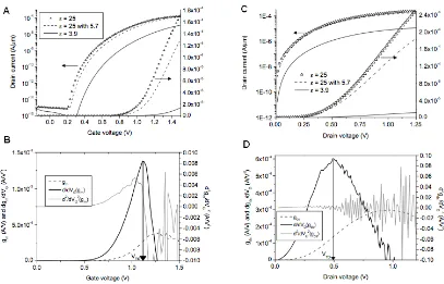
Figure 2-5: Double Gate n-type Si TFET (A) IDS–VGSin log (left axis) and linear (right axis)
scales for L = 50 nm εdielectric = 25; VDS = 1 V. (B) VTG extraction for L = 50 nm εdielectric = 25; VDS = 1 V
(C) IDS–VDSin log (left axis) and linear (right axis) scales for L = 50 nm εdielectric = 25; VGS = 1.5 V. (C)
VTD extraction for L = 50 nm εdielectric = 25; VGS = 1.5 V.[11]
Figure 2-5 shows VTG and VTD extracted from the IDS–VGS and IDS–VDS curves using the transconductance method. Plots A and C show IDS–VGS and IDS–VDS curves for a simulated TFET. Plots B and D shows the corresponding transconductance and
VTD was found to be 0.5 V, which was less than the VTG of 1.1 V. This relationship indicates that the TFET is more sensitive to the changes in the drain voltage than the gate
voltage.
One of the main limitations associated with a TFET is a low on-state current Ion. This low Ion is due to the band-to-band tunneling carrier injection mechanism. As the potential between the source and channel increases the band-to-band tunneling current is
less sensitive to the electric field [2]. Past the subthreshold region it is difficult to achieve
high Ion. There are several TFET device parameters that can be optimized to increase Ion. These parameters include lowering the bandgap of the material, adjusting the source
doping profile to be more abrupt, lowering the equivalent oxide thickness (EOT), and the
use of a double gate. The use of a lower bandgap material will improve the Ion since the tunneling current density is exponentially dependent on the bandgap as seen in Eq. 2-1.
For a Si-based device, adding a SiGe layer in the source region will increase the
band-to-band tunneling. Adding a SiGe layer to the entire active region will also increase Ion. However adding a SiGe layer to the entire active region will also increase the Ioff. This increase in off-state current will lower the Ion/Ioff current ratio[2]. The effect of a lower bandgap makes III-V materials an attractive option for TFETs.
For a TFET, an abrupt junction profile helps to increase Ion by decreasing the tunnel barrier width. This decrease in tunnel barrier width results in an increase in
tunneling probability. The addition of another gate on the TFET can lead to a doubling of
the gate oxide allows for the reduction of the EOT. Simulations of the TFET and different
dielectrics show the improvement in Ion with the introduction of high-κ dielectrics [2]. A majority of the published research on TFETs has been in the realm of
simulations [1, 5, 10, 12-14]. The conclusions of these simulations have to be viewed with
a certain degree of suspicion. The models that these simulations utilize have not been
calibrated with experimental data. Dr. Boucart in her thesis summed up the issue with the
current simulation tools.
“After the experience of using Silvaco Atlas for five years, I believe that
the non-local BTBT model gives good relative results when parameters are varied.
For example, when the gate dielectric constant is changed, we can get an idea of
how much the on-current will change relative to some reference device. On the
other hand, the absolute values of on-current, subthreshold swing, and threshold
voltage, are not calibrated. The on-current could be mis-estimated by two or more
orders of magnitude. This is an understandable situation when simulating
emerging devices, that for the moment still lack the adequate experimental data
necessary to calibrate these tools.” [1]
Experiential studies are needed in order to provide the data necessary for TFET model
calibration.
2.2 Experimentally Demonstrated TFETs:
A few groups have experimentally demonstrated TFETs. One of the earliest
reported TFETs was a gated p-i-n structure from Uemura et al. [15]. Uemura et al.
device as shown in Figure 2-6 was a GaAs p-i-n mesa with a GaAs/AlGaAs regrown gate along the mesa edge. The structure layers were grown via Molecular Beam Epitaxy
(MBE). The channel region of the device was directly doped with donors to improve the
peak tunneling current density to 3.7 µA/µm and enable a Peak-to-Valley Current Ratio
[image:27.612.230.454.234.467.2](PVCR) of 1.5 [15].
Figure 2-6: Channel Doped Surface Tunnel Transistor (CD-STT) Electrical Performance and Structure [15]
The CD-STT exhibited Negative Differential Resistance (NDR) and gate
modulation of the tunneling current. The NDR is indicative that tunneling is the current
transport mechanism. The shift in the I-V curves as the gate voltage is varied is indicative
of gate control.
Mookerjea et al. demonstrated a similar sidewall gated mesa approach to a TFET [16]. The Mookerjea device was an InGaAs based device with an Al2O3 and Pt/Au gate
Figure 2-7: TFET Family of curves Mookerjea, et al. [16]
As seen in Figure 2-7 the Mookerjea et al. structure also demonstrated NDR and gate control of the tunneling current. The Mookerjea et al. device had a peak Ion of 20 µA/µm and an off current at VDS= 50 mV of 40 pA/µm [16]. The subthreshold swing was found to be 150 mV/dec.
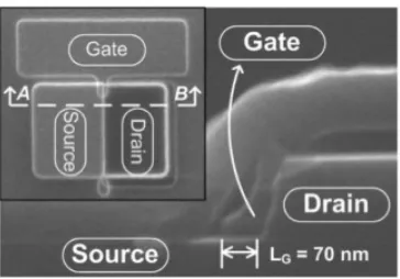
Choi et al. fabricated a 70 nm n-channel silicon TFET on silicon-on-insulator (SOI) substrate [2] at room temperature. Their device used the SOI layer as the insulating
region between the p+ source and the n+ drain. The channel length of the device was determined by the length of the SOI region. Figure 2-8 shows a SEM cross-section of the
Figure 2-8: Cross-sectional SEM image of the fabricated TFET when cutting through the A– B line. The gate length (LG) is measured to be 70 nm. The inserted figure shows the plan-view image.
[2]
The Choi TFET showed a sub-60 mV/dec subthreshold swing; however, the Ion of the device was low. The electrical performance of the Choi TFET can be seen in Figure
2-9.
Figure 2-9: Transfer curve of the fabricated TFET. The SS value is 52.8 mV/dec at room temperature. The ON and OFF currents were measured to be 12.1 µA/µm and 5.4 nA/µm, with the
power supply voltage at 1.0 V[2]
[image:29.612.249.429.379.549.2]The value of Ioff for the device was found to be larger than expected for a TFET. The larger Ioff is attributed to drain-to-gate leakage current [2].
The similarity between these devices is a gated mesa sidewall approach. The
vertical mesas are a result of the MBE to grow highly doped and ultra sharp junctions. All
of the mesas are formed during an isolation etch. The isolation etch is often a
crystallographic wet etch. The etch results in a sloped profile along the mesa. While this
structure allows for the alignment of the gate along the junction it also results in a large
overlap of the gate to the drain of the device. This gate overlap as seen in Figures 2-6 and
2-8 result in a gate-to-drain leakage current. This leakage current results in a lower Ioff. Further adding to the drain-to-gate leakage current is the thin gate oxide. Since the gate
oxide is also used to separate the gate and drain, as the gate oxide is thinned down to
improve gate control the overlap between the gate and drain becomes more serious. A
solution to this problem is the addition of a barrier layer on top of the drain [15]. This
barrier layer helps further isolate the gate from the drain. The barrier layer can be
selectively etched to allow for contact to the drain. The barrier layer is one of several
design considerations that need to be made for a TFET.
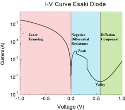
2.3 Esaki Diode
Esaki diodes are tunnel diodes with a very abrupt and degenerately doped pn or
p-i-n junction. The general difference between an Esaki diode and a TFET is that the Esaki
diode lacks a gate across the junction and a thinner i-region. This thin abrupt junction
causes the conduction bands of the two doped regions to overlap. This overlap allows for
bias on the Esaki diode results in Zener tunneling. When a forward bias is applied there is
a forward tunneling component where the current increases with forward bias. At a certain
point the current drops as forward bias is increased. The maximum current value before
the current begins to decrease is referred to as the peak tunneling current. The current
continues to degrade as the voltage is increased until the forward applied bias reaches a
certain value where the current will begin to increase again. The minimum current before
the current begins to increase again is referred to as the valley current. The region where
forward bias is increased yet the current decreases is referred to as negative differential
resistance. Negative differential resistance is a key characteristic of an Esaki diode. In
this region of negative differential resistance, tunneling is the main current transport
mechanism. The current decreases as forward bias is applied due to the conduction bands
passing each other as the forward bias is increased. As the conduction bands separate from
each other the degree of tunneling decreases. Following the valley point diffusion current
is the current transport mechanism. Figure 2-10 shows these different regions of
Figure 2-10: Esaki Diode Regions of Operation
Esaki diode performance is evaluated utilizing the Peak-to-Valley Current Ratio
(PVCR). A high PVCR is desirable for logic applications and noise margin performance.
The higher the PVCR the more robust a device is against noise in the input signal. In
general for logic applications a PVCR of 2.0 is needed. The PVCR is the ratio of the peak
tunneling current to the lowest tunneling current when forward bias is applied to an Esaki
diode. Eq. 2-9 shows the equation used to calculate PVCR.
PVCR
=
J
PJ
V (2-9)As seen in Figure 2-10, the peak tunneling current is the max current at the onset
of negative differential resistance; the valley current is the current level when diffusion
Chapter 3
Process Details
This work utilizes two different process approaches to study tunneling devices.
The mesa-first process has been developed to fabricate TFETs and gated tunneling
devices. The metal-first process has been used to fabricate sub-micron Esaki diodes [3],
the result of the metal-first process will be used as a baseline to compare with the
mesa-first process. Both approaches rely on creating a mesa out of a heavily doped p-i-n layer. These mesas become the individual tunneling devices. The metal-first process defines the
mesa by first depositing a metal contact and then using this contact as the etch mask for
the mesa. The mesa-first process differs in that a removable etch mask is used to define
the mesa. The removable mask allows for the sidewalls of the mesa to be easily gated. The
sidewall gate runs across the vertical p-i-n junction, thus adding control to a tunnel junction. Section 3.1 will detail every step of the mesa-first process flow. Section 3.2 will
detail the metal-first Esaki diode process used to calibrate the tunneling structures.
3.1 Mesa-First Process Flow
The mesa-first process was designed to be flexible across multiple material
systems: InGaAs, SiGe, GaSb, and InAs. These different material systems have
individual requirements for example; compatible contact materials and temperature limits.
Therefore individual process steps may differ for different material systems. This process
was originally developed for InGaAs. The process steps listed below correspond to
InGaAs based devices. The modular nature of this process means that it can be easily
adapted to multiple material systems. All that is needed is a check of material
compatibility, etch chemistry, and thermal budget constraints.
3.1.1 Surface Preparation
A clean surface is critical for the mesa-first process flow. The individual samples
that the devices are fabricated on average 0.6 x 0.7 cm in dimension. These samples are
cleaved from a wafer with a p-i-n junction epitaxially grown on top of an InP substrate. Cleaving a sample results in particles on top of the device surface. These may cause
defects in subsequent lithography and etch steps. A post-cleave IPA rinse is used to clean
the top of the sample. If there is no sacrificial layer to be stripped from the top of the
sample, it is ready for the first lithography step.
A p-i-n layer structure may be grown with an undoped etch cap. This undoped cap serves as a sacrificial layer to protect the top of the p-i-n junction. Typically an InP etch cap is used for an InGaAs-based device. The InP etch cap allows it to be selectively
between the gate and the drain of the device. The InP etch cap etch is removed in an
HCL:H2O (1:1) solution. The HCL:H2O (1:1) is selective to the InGaAs [17]. To verify
that the etch cap is completely removed a simple ohmmeter may be used. The undoped
etch cap typical measures in the MΩ range while the top of the device structure is in the
tens of Ω range.
3.1.2 Mesa Definition Lithography
The first lithography step is the most critical as it defines the TFET mesas. The
lithography is performed on a LEO EVO 50 Scanning Electron Microscope (SEM) with
the Nanometer Pattern Generation System (NPGS). This direct write Electron Beam
Lithography (EBL) system was used to define the mesas in MaN 2401. MaN 2401 is an
electron-beam-sensitive negative resist which, when exposed, developed, and cured, is
resistant to etch chemistry and is removable by an O2 plasma.
Mesa lithography begins with the sample being first submerged in SurPass 3000
for 30 seconds. The sample is then rinsed in deionized water for 30 seconds. The samples
are then spun dry at 1500 RPM for 30 seconds. The MaN 2401 resist is then applied and
spun coat at 1500 RPM for 60 seconds. The sample is then baked at 90°C for 60 seconds.
The sample is then mounted to the SEM’s sample holder. Special attention must be given
to the cleanliness of the sample holder and the back of the sample. As the sample is
secured to the mount, any macroscopic particle on the back of the sample or piece holder
may cause the sample to break. The first level EBL defines a series of mesas ranging
from mask-defined widths of 150 nm to 2µm. Table 3-1 contains the magnification,
Parameter Value
Magnification 150X
Center-to-Center Spacing 56.20 nm
Line Spacing 56.20 nm
Dose 210 µC/cm2
[image:36.612.111.527.61.324.2]Mask Level 1
Table 3-1: Level 1 Electron Beam Lithography Job Parameters
Figure 3-1: First Level Lithography – Mesa Definition
Following exposure the sample is developed in a bath of CD-26 developer for 60 seconds.
A subsequent develop step in a new bath of CD-26 is performed for 15 seconds. The
sample is rinsed and dried. Following a microscope inspection the piece is baked at 100°C
for 60 seconds. Figure 3-1 shows a cross section of the device after mesa definition
lithography.
3.1.3 Mesa Etch
The mesa etch for InGaAs is a wet etch utilizing citric acid (C6H8O7). The etch
chemistry is C6H8O7:H2O:H2O2 (20:20:1). The etch rate is dependent on the layer
structure of the device and the doping of the individual layers. Undoped layers will etch at
a slower rate then doped regions. Profilometry measurement before, during and after the
etch are taken to calculate etch rates and a final etch depth. Figure 3-2 shows the cross
Figure 3-2: Mesa Etch
3.1.4 MaN Resist Strip
Following the mesa etch the MaN 2401 resist mask is removed. The mask is
removed via oxygen plasma etch. The Lam 490 AutoEtch was utilized to remove the MaN
2401 resist. The plasma recipe developed for this etch uses 100 sccm of O2 at a power of
100 W. Table 3-2 contains the full etch recipe details. Figure 3-3 shows the cross section
of the device after the resist etch. SEM inspection is utilized to verify that the MaN resist
has cleared.
Parameter Value
Pressure 300 mtorr
Gap Spacing 1.65 cm
O2 Flow 100 sccm
RF Power 100 W
Time 2 minutes
Figure 3-3: MaN 2401 Resist Strip
The resist strip was found to fully clear most of the resist. However it was found
that the MaN resist was susceptible to contamination. For example if the MaN resist is not
fully cured and exposed to chlorine-based chemistry such as HCl, the resist forms a
residue that is difficult to remove. Figure 3-4 shows the residue remaining after a plasma
treatment.
Figure 3-4: Contaminated MaN 2401 - After 2 minutes O2 plasma
To fully remove this resist residue, fluorine was added to the plasma etch chemistry. A
3.1.5 Gate Stack Deposition
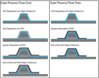
The TFET gate stack is deposited through Atomic Layer Deposition (ALD) and
reactive sputtering. The gate stack consists of a high-k dielectric and a refractory gate
metal. The main limitation in this body of work was the lack of ALD onsite at Rochester
Institute of Technology. The ALD deposition performed in this work was done at The
Pennsylvania State University and at SEMATECH. Al2O3 is deposited as the gate oxide
through the ALD. The gate oxide thickness is targeted at 6-10 nm.
The refractory gate metal was deposited either by ALD deposition or via a reactive
sputtering. TaN and TiN are used as the gate metal. An ALD gate metal such as TiN has
an advantage in that it is deposited after the gate oxide without having to break vacuum.
This helps ensure a high quality metal dielectric interface. However, the TiN that is
deposited via ALD is limited in thickness to between 10 nm and 100 nm. ALD-deposited
TiN requires a subsequent deposition of a much thicker material for a gate contact. For
this role TaN can be reactively sputtered. Further, if ALD gate metal is unavailable TaN
Figure 3-5: Gate Process Flows
Gate process flow one calls for the deposition of Al2O3 followed by deposition of
TiN using ALD. An EBL lift-off process is used to define where TaN will be reactively
sputtered to add more gate material. This second level EBL step defines the shape and
location of the gate. For the EBL lift-off process a LOR5A PMMA resist stack is coated
Step Description Spin Speed [RPM] Time [Seconds]
1 Apply LOR5A
2a) Spin Coat LOR5A – Ramp 0-500 2
2b) Spin Coat LOR5A – Steady State 500 2
2c) Spin Coat LOR5A – Ramp 500-4000 2
2d) Spin Coat LOR5A – Steady State 4000 45
3 Apply PMMA
4a) Spin Coat PMMA – Ramp 0-500 2
4b) Spin Coat PMMA – Steady State 500 2
4c) Spin Coat PMMA – Ramp 500-4000 2
4d) Spin Coat PMMA – Steady State 4000 45
Table 3-3: Gate Level EBL LOR5A/PMMA Resist Coat Recipe
The PMMA/LOR5A resist stack is then baked at 180°C for 10 minutes. The sample is
then mounted on a piece holder and loaded into the SEM. The second level alignment and
electron beam lithography is performed using the NPGS system. Table 3-4 contains the
magnification spacing information and dose information.
Parameter Value
Magnification 150X
Center-to-Center Spacing 56.20 nm
Line Spacing 56.20 nm
Dose 300 µC/cm2
Mask Level 2
Table 3-4: Gate Level Electron Beam Lithography Job Parameters
The TaN reactive sputter is performed using the PE4400 using the deposition
recipe as outlined in Table 3-5, with a deposition time of 20 minutes. Submerging the
sample in a heated bath of Remover PG then lifts off the excess TaN. Following the lift
off the exposed TiN is etched using a CF4 plasma. The exposed Al2O3 is etched away in a
Parameter Value
Target Material Tantalum
Base Pressure 1.0x10⁻⁷ Torr
Deposition Pressure 2 mTorr
N2 1.85 sccm
Ar 35 sccm
Rotation Speed 2.4 RPM
RF Power 400 W
Table 3-5: PE4400 TaN Sputter Deposition Recipe
The alternative gate process flow or gate process flow two does not incorporate the TiN
deposition or etch. The TaN is used directly as the gate metal and is defined and deposited
using the same procedure.
3.1.6 Benzocyclobutene (BCB) Deposition
BCB is utilized as an Inter Layer Dielectric (ILD) to support the top contact. This
process was developed using BCB from Dow Chemical, CYCLOTENE 3022-35. The
BCB was deposited through a spin coat process. For adequate adhesion of the BCB a
clean surface is required. The sample surface is first cleaned with an isopropyl alcohol
followed by a rinse in deionized H2O and a dehydration bake. The sample is then treated
with the adhesion promoter AP3000. The BCB is then spin coated, followed by a soft
Step Description Spin Speed [RPM] Time [Seconds]
1 Apply AP3000
2 Spin Coat AP3000 1000 60
3 Apply BCB
4a) Spin Coat BCB – Ramp 0-500 2
4b) Spin Coat BCB – Steady State 500 2
4c) Spin Coat BCB – Ramp 500-4000 2
4d) Spin Coat BCB – Steady State 4000 2
4e) Spin Coat BCB – Ramp 4000-5000 2
4f) Spin Coat BCB – Steady State 5000 60
Table 3-6: BCB Spin Coat Recipe
Following the spin coat, the BCB is cured in a two-part bake procedure. During
the cure it is critical that the BCB is not heated above 150°C in an oxygen ambient. At
temperatures above 150°C, the BCB in the presence of oxygen can oxidize. The sample is
first baked on a hot plate for 10 minutes at 140°C to help set the BCB. The BCB is then
cured at 250°C for 1 hour in the Blue M box oven with a nitrogen ambient. The sample is
loaded into the oven at a temperature of 140°C. The piece is held at a soak of 140°C for
10 minutes with nitrogen flowing. The temperature is then ramped to 250°C and then held
at 250°C for 1 hour. Following the 1-hour cure the temperature is ramped down to 140°C
before the piece is removed. Figure 3-6 shows the cross section of the device following
the BCB coat.
A blank silicon piece of similar size should be co-processed during this step. This
silicon piece is coated with BCB and baked with the device sample. This piece is used to
3.1.7 BCB Etch Back
The BCB process results in a significant amount of overburden. This overburden
inhibits contacting the top of the mesas. The BCB is thus etched back to clear the top of
the mesa. The BCB is etched back in an O2: SF6 (4:1) plasma. The etch rate is dependent
on the power used and the BCB cure cycle. Slight variations in the BCB cure cycle can
cause the etch rate to vary by 20%. The BCB etch is performed in the Lam 490 AutoEtch
using the etch recipe describe in Table 3-7.
Parameter Value
Pressure [mtorr] 300
Gap Spacing [cm] 1.65
O2 Flow [sccm] 80
SF6 Flow [sccm] 20
RF Power [W] 25-50
Time [minutes] 2
Table 3-7: BCB Etch Back Lam 490 AutoEtch Recipe
The BCB etch back begins with a calibration of etch rates using the BCB coated silicon
test piece. The BCB thickness on the silicon piece is measured with a Nanospec, by
setting the Index of Refraction (n) to 1.54. The BCB silicon test piece is then etched for 1
minute at 50 W. The remaining BCB thickness is measured and the etch rate for 50 W is
calculated. The BCB is then etched for a minute at 25 W. The remaining BCB thickness is
measured and the etch rate for 25 W is calculated. These two etch rates will be used to
calculate the BCB etch time for the device sample.
The BCB thickness on the device sample is measured using a point between
different die. With the BCB thickness data, the measured mesa height, and the previously
calculated etch rates, the time needed to etch the BCB to just above the top of the mesa is
are then taken to verify the thickness of remaining BCB. A second etch at 25 W is used to
place the final BCB thickness a few nm below the top of the mesa. The calibrated 25 W
etch rate along with the remaining BCB thickness and the mesa height is taken into
account to calculate the second etch time. Figure 3-7 shows the cross section of the device
after the BCB etch back.
Figure 3-7: BCB Etch Back
Following the second etch measurements are taken with the Nanospec to verify the
final BCB thickness. To insure that the BCB has cleared the top of the mesas, the samples
are placed in the SEM. The criterion for a successful etch back is a final BCB thickness
less than the top of the mesa but 10 nm above the top of the i-region. This insures that the BCB is sufficiently isolating the junction. If the BCB was over-etched a plasma etch is
performed to completely remove the BCB and the sample is reworked.
3.1.8 BCB Via Etch Lithography
The BCB is now isolating the top of the device from the i-region, the gate contact and the substrate. Vias through the BCB are needed to contact gate and the substrate. The
LOR5A/PMMA resist mask as etch mask. The LOR5A and PMMA are spin coated using
the recipe listed in Table 3-8
Step Description Spin Speed [RPM] Time [Seconds]
1 Apply LOR5A
2a) Spin Coat LOR5A – Ramp 0-500 2
2b) Spin Coat LOR5A – Steady State 500 2
2c) Spin Coat LOR5A – Ramp 500-4000 2
2d) Spin Coat LOR5A – Steady State 4000 45
3 Apply PMMA
4a) Spin Coat PMMA – Ramp 0-500 2
4b) Spin Coat PMMA – Steady State 500 2
4c) Spin Coat PMMA – Ramp 500-4000 2
4d) Spin Coat PMMA – Steady State 4000 45
Table 3-8: BCB Via Etch LOR5A/PMMA Resist Coat Recipe
The PMMA/LOR5A resist stack is then baked at 180°C for 10 minutes. The sample is
then mounted on a piece holder and loaded into the SEM. The via etch level alignment
and electron beam lithography is performed using the NPGS system. Table 3-9 contains
the magnification spacing information and dose information
Parameter Value
Magnification 150X
Center-to-Center Spacing 56.20 nm
Line Spacing 56.20 nm
Dose 300 µC/cm2
Mask Level 3
Table 3-9: Level 3 Electron Beam Lithography Job Parameters
Following exposure the piece is developed in MIBK:IPA 1:3 for 2 minutes. A subsequent
develop step in a new bath of CD-26:H2O (1:1) is performed for 2 minutes. A final
develop in CD-26 for 10 seconds is performed. The sample is rinsed and dried. Figure 3-8
Figure 3-8: Level 3 Lithography- Via Etch
3.1.9 BCB Via Etch
The BCB via etch is performed using the Lam 490. The via plasma etch chemistry
is the same etch as that which is used for the etch back. The etch recipe for the via etch
can be found in Table 3-7, with the etch being performed at 50 W. The etch time is
determined by the remaining BCB thickness and the previously calculated etch rates. In
general this etch is on the order of a few seconds. Following the etch Nanospec
measurements are taken within the via etch to verify that the remaining BCB is gone.
Dark-field microscope inspection is also useful in verifying that the remaining BCB is
removed from the vias. Once it is verified that the vias are clear, the sample is placed in a
bath of Remover PG for 5 minutes. The Remover PG removes the remaining resist etch
Figure 3-9: BCB Via Etch
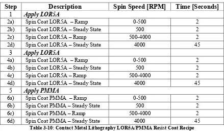
3.1.10 Contact Metal Lithography and Deposition
Gold (Au) is utilized as the contact metal for the InGaAs based device. The first
step is to define the regions where the contact metal will be deposited through an EBL
lift-off process. This process uses a LOR5A/PMMA resist stack. The LOR5A is spin coated
twice followed PMMA. The spin coat the recipe is listed in Table 3-10
Step Description Spin Speed [RPM] Time [Seconds]
1 Apply LOR5A
2a) Spin Coat LOR5A – Ramp 0-500 2
2b) Spin Coat LOR5A – Steady State 500 2
2c) Spin Coat LOR5A – Ramp 500-4000 2
2d) Spin Coat LOR5A – Steady State 4000 45
3 Apply LOR5A
4a) Spin Coat LOR5A – Ramp 0-500 2
4b) Spin Coat LOR5A – Steady State 500 2
4c) Spin Coat LOR5A – Ramp 500-4000 2
4d) Spin Coat LOR5A – Steady State 4000 45
5 Apply PMMA
6a) Spin Coat PMMA – Ramp 0-500 2
6b) Spin Coat PMMA – Steady State 500 2
6c) Spin Coat PMMA – Ramp 500-4000 2
6d) Spin Coat PMMA – Steady State 4000 45
Table 3-10: Contact Metal Lithography LOR5A/PMMA Resist Coat Recipe
The PMMA/LOR5A resist stack is then baked at 180°C for 10 minutes. The sample is
performed using the NPGS system. Table 3-11 contains the magnification spacing
information and dose information.
Parameter Value
Magnification 150X
Center-to-Center Spacing 56.20 nm
Line Spacing 56.20 nm
Dose 300 µC/cm2
Mask Level 4
Table 3-11: Level 4 Electron Beam Lithography Job Parameters
Following exposure the piece is developed in MIBK:IPA 1:3 for 2 minutes. A subsequent
develop step in a new bath of CD-26:H2O (1:1) is performed for 2 minutes. A final
develop in CD-26 for 10 seconds is performed. The sample is rinsed and dried.
The sample is then loaded into the Nano 38 thermal evaporator. For the contact
metal 2000 Å of Au is deposited. The sample is then placed into a heated bath of Remover
PG. After the Au is lifted off the piece is placed into another bath of Remover PG. This
second bath is utilized to remove any lift-off resist residue. Figure 3-10 shows the cross
section of the device after Level 3 lithography and Au deposition. The device after this
Figure 3-10: Final Cross Section
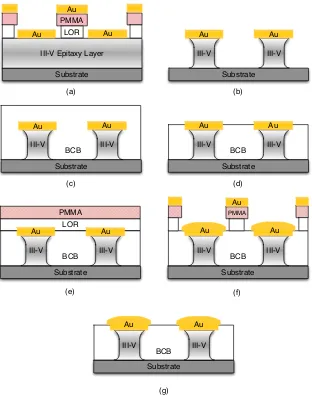
3.2 Metal-First Esaki Diode Process Flow
The metal-first Esaki diode process utilizes EBL to fabricate a series of small
diameter devices between 100 nm and 40 micron. This approach can be seen in Figure
3-11. The process utilizes an (a) E-beam lift-off lithography process to define the initial gold
contacts. This is followed by (b) wet isolation etch utilizing the gold contact as an etch
mask. (c) Bisbenzocyclobutene (BCB) is coated to isolate the tunnel diodes and support
the gold contacts. (d) The BCB is plasma-etched back to remove the overburden. (e) The
sample is then coated with LOR5A and PMMA. (f) The sample is aligned and second
level lithography is performed to define larger probe contacts. Following a gold contact
Figure 3-11: Metal-first Esaki Diode Process
The metal-first process shares many features with the mesa-first process. While
using different mask designs, the process modules are the same. Table 3-12 highlights the
corresponding process modules and changes between the two processes.
LOR Substrate III-V Epitaxy Layer
Substrate Substrate PMMA Substrate BCB BCB (a) (b) (c) (e) (d) PMMA Au
Au LOR Au
Metal-first Process Corresponding Mesa-first Process Amendments.
Level 1 Metal Definition Coat & Write conditions from 3.1.8 New Mask File
Mesa Etch 3.1.3
BCB 3.1.6
BCB Etch Back 3.1.7
Level 2 Metal Definition 3.1.10 New Mask File
Table 3-12: Metal-first Process Details
To extract the electrical performance of the Esaki diodes, a methodical testing
approach has been developed. Following the initial wet isolation etch, SEM cross-sections
are taken to assess the undercut for each of the different diode sizes. The cross-sections
are taken in both etch planes. Top-down SEM measurements are taken across the sample
to measure the area of the gold contact. The measurements across the sample allow for
e-beam variations to be corrected for in the effective area calculations. The top-down SEM
micrographs are put through image-processing routines to calculate the area of the gold
contacts. Using the area and undercut profile information, effective device areas are
calculated. This corrected area is used in the current density calculations. Following
fabrications the devices undergo extensive electrical testing. Data analysis is performed on
the IV curves to extract series resistance, contact resistance, PVCR, Vpeak, Jpeak, and Vvalley.
3.3 Mesa-first TFET Layout
EBL is used to define deep submicron mesas in the p-i-n structure, the wrap-around gates, via and top contacts. The mask design used for the EBL processes, is
defined using Design CAD LT. The mask design is a single file containing all of the
layout information for one die. The layout consists of numerous devices, including gated
The basic layout for all gated devices is the same. The layout for a single TFET
calls for a rectangular mesa. A wrap-around gate is applied across the rectangular mesa. A
contact is used to contact the top of the device. For the TFET size of the mesa, the number
and area of the gates and contacts is varied. Figure 3-12 shows the masked defined view
of a TFET and a cross section of the device corresponding to a cutline through the middle
device. This design is based upon four layers, which correspond to the different
[image:53.612.131.517.268.527.2]lithography steps.
Figure 3-12: Individual TFET Layout
The layout contains four layers. Level 1 defines the mesa and alignment marks used for
subsequent lithography steps. Level 2 defines the gate across the mesa. Level 3 defines
vias in the BCB to contact the gate and the substrate layers. Layer 4 defines the top
contact metal. The whole layout with multiple gated devices, non-gated diodes, and test
Figure 3-13: TFET Test Structure Die Level Layout
As seen in Figure 3-13 each die is centered around alignment “L’s”. These are alignment
marks defined during the first level lithography. The NPGS system scans for these
alignment marks during later levels to align each individual die. Also situated on the
mask design is a series of non-gated diodes. These mesa-first tunnel diodes are used to
compare the fabrication process with that of tunnel diodes fabricated using a metal-first
scheme. The gated test structure is used to verify that the gate is conformal over the
Chapter 4
Process Module Development
This chapter will focus on development of selected process modules needed to
fabricate a mesa-first TFET. The following process modules are essential to the mesa-first
process and provide additional details beyond what was described in Chapter 3. Section
4.1 will discuss electron beam lithography and alignment. Section 4.2 will cover BCB
deposition and curing. Section 4.3 will discuss plasma etch of BCB. Section 4.4 will
4.1 Electron Beam Lithography
Electron Beam Lithography (EBL) enables the fabrication of nanometer-scale
devices without the need for expensive Excimer laser based systems. EBL’s advantages
lay in its resolution and flexibility. EBL has resolution limit between 10-20 nm. EBL,
unlike optical lithography, does not require a mask to define a pattern. Instead EBL is a
direct write process. EBL systems direct an electron beam point by point to define a
pattern in an electron-sensitive resist. The lack of a physical mask enables quick
prototyping of devices by allowing for easy design changes. However this quick
prototyping comes at the cost of EBL’s low throughput. Thus EBL is limited to research
and development applications and low-volume production.
The mesa-first process uses EBL for its versatility and its ability to easily write
small pieces. Due to the limited supply of III-V semiconductor samples, the individual
piece size is limited to 0.6 x 0.7 cm. This small size limits the options for lithography.
Optical projection-based steppers require special piece chucks to secure such small
samples. The NPGS EBL system at RIT where this work was performed already has the
capability to write on small pieces. NPGS is a standalone system, which modifies the LEO
EVO 50 SEM and transforms it into an EBL system. NPGS works by controlling the stage
movements and the blanking of the electron beam to write the specified patterns.
Overlay precision is critical for the mesas first process. At the second level and
beyond, EBL is dependent on proper alignment. NPGS has the capability to perform
automatic and assisted manual alignment. To do so NPGS requires the DesignCad mask
file, alignment spacing information, and clear alignment marks. NPGS reads the Design
looks for are those which were transferred into the sample by previous EBL steps. Using
the alignment spacing information, NPGS can automatically search for alignment marks,
identify the marks with the mask file, and align the die for the write.
There are two sets of alignment marks utilized for alignment, the global alignment
marks and die alignment marks. The global alignment marks are a 3x3 array of crosses
used to correct for global rotational errors. The die alignment marks are the four “L”
shaped alignment marks that are on the corner of each device die. Figure 4-1 shows how
[image:57.612.109.542.321.653.2]NPGS writes the die and global alignment marks on the sample.
The location of the global alignment marks is determined by the size of the device array.
As seen in Figure 4-1 the 3x3 global alignment mark array is aligned to the center of the
sample. The device array is offset to be inside the global alignment array. The numbers of
columns and rows of the device array are constrained by the size of the die, the spacing
between die, and the active area of the sample. These constraints are taken into account
per sample to determine the size of the array that will fit within the active area. Eq. 4-1
and Eq. 4-2 show how the global alignment mark spacing is calculated as a function of the
device array and the die spacing.
YGlobal Alignment Spacing
[ ]
um =Number of Rows × YDie Spacing
[ ]
um2 +300
[ ]
um (4-1)XGlobal Alignment Spacing
[ ]
um =Number of Columns × XDie Spacing
[ ]
um2 +300
[ ]
um (4-2)Recording the device array size, die spacing, and corresponding global alignment spacing
is critical for second level alignment. The NPGS requires this information to search for the
die level alignment marks.
The alignment procedure is two-fold. Using the SEM control, an outer corner
global alignment mark is found. A SEM stage move corresponding to the Y Global Alignment
Spacing is used to bring a center edge global alignment mark into focus. The alignment cross
is then centered in the SEM field of view. A stage shift of -Y Global Alignment Spacing in the y-axis is performed. The lower alignment mark is centered in the SEM field of view by only
center edge alignment mark is centered in the SEM field of view by using only x and y
translational adjustments. The procedure is repeated until a stage shift in either direction
results in the global alignment marks being centered in the SEM field of view. The stage
is then shifted to the center global alignment cross. The SEM is then handed over to the
NPGS system. When the EBL job is started NPGS begins the individual die alignment.
There is an issue with NPGS system at RIT. Since the NPGS is a stand alone
system, it requires a separate computer, digital-to-analog converter, and cabling to
i
![Figure 2-4: Simulated band diagram for a 100nm n-channel silicon TFET with p+ δ-doped SiGe layer between the p+ source and insulating region [10]](https://thumb-us.123doks.com/thumbv2/123dok_us/49389.4484/22.612.251.432.77.249/figure-simulated-diagram-channel-silicon-source-insulating-region.webp)
![Figure 2-6: Channel Doped Surface Tunnel Transistor (CD-STT) Electrical Performance and Structure [15]](https://thumb-us.123doks.com/thumbv2/123dok_us/49389.4484/27.612.230.454.234.467/figure-channel-surface-tunnel-transistor-electrical-performance-structure.webp)