Manufacturing with light - micro-assembly of
opto-electronic microstructures
S
HUAILONGZ
HANG,
1,2,9Y
ONGPENGL
IU,
1,3Y
ANGQ
IAN,
1W
EIZHENL
I,
1J
OANJ
UVERT,
4,5P
ENGFEIT
IAN,
6J
EAN-C
LAUDEN
AVARRO,
7A
LASDAIRW C
LARK,
1E
RDANG
U,
8M
ARTIND. D
AWSON,
8J
ONATHANM. C
OOPER,
1 ANDS
TEVENL. N
EALE1,101School of Engineering, University of Glasgow, Glasgow, Scotland, G12 8LT, UK
2Current address: Department of Chemistry, University of Toronto, Toronto, Ontario, M5S 3H6, Canada 3Current address: Laboratory for Molecular Engineering of Optoelectronic Nanomaterials, Institute of
Chemical Sciences and Engineering, École Polytechnique Fédérale de Lausanne, CH-1015 Lausanne, Switzerland
4Photonics Research Group, INTEC, Ghent University-IMEC, iGent Tower, 9052 Ghent, Belgium 5Center for Nano- and Biophotonics, Ghent University, iGent Tower, 9052 Ghent, Belgium 6Institute for Electric Light Sources, Fudan University, Shanghai, 200433, China
7IPS, 24A, rue de la Résistance, BP 438, 74108 ANNEMASSE Cedex, France
8Institute of Photonics, Deparment of Physics, University of Strathclyde, Glasgow, Scotland, G1 1RD, UK 9[email protected]
Abstract: Optical micromanipulation allows the movement and patterning of discrete micro-particles within a liquid environment. However, for manufacturing applications it is desirable to remove the liquid, leaving the patterned particles in place. In this work, we have demonstrated the use of optoelectronic tweezers (OET) to manipulate and accurately assemble Sn62Pb36Ag2 solder microspheres into tailored patterns. A technique based on freeze-drying technology was then developed that allows the assembled patterns to be well preserved and fixed in place after the liquid medium in the OET device is removed. After removing the liquid from the OET device and subsequently heating the assembled pattern and melting the solder microspheres, electrical connections between the microspheres were formed, creating a permanent conductive bridge between two isolated metal electrodes. Although this method is demonstrated with 40 µm diameter solder beads arranged with OET, it could be applied to a great range of discrete components from nanowires to optoelectronic devices, thus overcoming one of the basic hurdles in using optical micromanipulation techniques in a manufacturing micro-assembly setting.
Published by The Optical Society under the terms of theCreative Commons Attribution 4.0 License. Further distribution of this work must maintain attribution to the author(s) and the published article’s title, journal citation, and DOI.
OCIS codes:(350.4855) Optical tweezers or optical manipulation; (120.4610) Optical fabrication; (120.4880) Optome-chanics.
References and links
1. A. Ashkin, J. M. Dziedzic, and T. Yamane, “Optical trapping and manipulation of single cells using infrared laser beams,” Nature330(6150), 769–771 (1987).
2. D. G. Grier, “A revolution in optical manipulation,” Nature424(6950), 810–816 (2003).
3. L. Paterson, M. MacDonald, J. Arlt, W. Sibbett, P. Bryant, and K. Dholakia, “Controlled rotation of optically trapped microscopic particles,” Science292(5518), 912–914 (2001).
4. M. Zhong, X. Wei, J. Zhou, Z. Wang, and Y. Li, “Trapping red blood cells in living animals using optical tweezers,” Nat. Comm.4, 1768 (2013).
5. X. Ding, Z. Peng, S.-C. S. Lin, M. Geri, S. Li, P. Li, Y. Chen, M. Dao, S. Suresh, and T. J. Huang, “Cell separation using tilted-angle standing surface acoustic waves,” Proc. Natl. Acad. Sci. U.S.A.111(36), 12992–12997 (2014). 6. F. Guo, Z. Mao, Y. Chen, Z. Xie, J. P. Lata, P. Li, L. Ren, J. Liu, J. Yang, M. Dao, S. Sureshd, and T. J. Huang,
“Three-dimensional manipulation of single cells using surface acoustic waves,” Proc. Natl. Acad. Sci. U.S.A.113(6), 1522–1527 (2016).
#302543 https://doi.org/10.1364/OE.25.028838
7. R. Pethig, “Dielectrophoresis: Status of the theory, technology, and applications,” Biomicrofluidics4(2), 022811 (2010).
8. P. Y. Chiou, A. T. Ohta, and M. C. Wu, “Massively parallel manipulation of single cells and microparticles using optical images,” Nature436(7049), 370–372 (2005).
9. A. T. Ohta, M. Garcia, J. K. Valley, L. Banie, H.-Y. Hsu, A. Jamshidi, S. L. Neale, T. Lue, and M. C. Wu, “Motile and non-motile sperm diagnostic manipulation using optoelectronic tweezers,” Lab Chip10(23), 3213–3217 (2010). 10. S. M. Yang, T. M. Yu, H. P. Huang, M. Y. Ku, L. Hsu, and C. H. Liu, “Dynamic manipulation and patterning of
microparticles and cells by using TiOPc-based optoelectronic dielectrophoresis,” Opt. Lett.35(12), 1959–1961 (2010).
11. A. Zarowna-Dabrowska, S. L. Neale, D. Massoubre, J. McKendry, B. R. Rae, R. K. Henderson, M. J. Rose, H. Yin, J. M. Cooper, E. Gu, and M. M. Dawson, “Miniaturized optoelectronic tweezers controlled by GaN micro-pixel light emitting diode arrays,” Opt. Exp.19(3), 2720–2728 (2011).
12. S. L. Neale, A. T. Ohta, H. Y. Hsu, J. K. Valley, A. Jamshidi, and M. C. Wu, “Trap profiles of projector based optoelectronic tweezers (OET) with HeLa cells,” Opt. Exp.17(7), 5231–5239 (2009).
13. W. Choi, S. W. Nam, H. Hwang, S. Park, and J. K. Park, “Programmable manipulation of motile cells in optoelectronic tweezers using a grayscale image,” Appl. Phys. Lett.93(14), 143901 (2008).
14. J. K. Valley, S. Neale, H. Y. Hsu, A. T. Ohta, A. Jamshidi, and M. C. Wu, “Parallel single-cell light-induced electroporation and dielectrophoretic manipulation,” Lab Chip9(12), 1714–1720 (2009).
15. H. Hwang and J. K. Park, “Optoelectrofluidic platforms for chemistry and biology,” Lab Chip11(1), 33–47 (2011). 16. M. Woerdemann, C. Alpmann, M. Esseling, and C. Denz, “Advanced optical trapping by complex beam shaping,”
Laser Photon. Rev.7(6), 839–854 (2013).
17. A. Jamshidi, P. J. Pauzauskie, P. J. Schuck, A. T. Ohta, P. Y. Chiou, J. Chou, P. Yang, and M. C. Wu, “Dynamic manipulation and separation of individual semiconducting and metallic nanowires,” Nat. Photon.2(2), 86–89 (2008). 18. P. J. Pauzauskie, A. Jamshidi, J. K. Valley, J. H. Satcher Jr, and M. C. Wu, “Parallel trapping of multiwalled carbon
nanotubes with optoelectronic tweezers,” Appl. Phys. Lett.95(11), 113104 (2009).
19. A. Jamshidi, S. L. Neale, K. Yu, P. J. Pauzauskie, P. J. Schuck, J. K. Valley, H. Y. Hsu, A. T. Ohta, and M. C. Wu, “Nanopen: Dynamic, Low-power, and Light-actuated Patterning of Nanoparticles,” Nano Lett.9(8), 2921–2925 (2009).
20. S. Zhang, Y. Liu, J. Juvert, P. Tian, J. C. Navarro, J. M. Cooper, and S. L. Neale, “Use of optoelectronic tweezers in manufacturing - accurate solder bead positioning,” Appl. Phys. Lett.109(22), 221110 (2016).
21. S. Zhang, J. Juvert, J. M. Cooper, and S. L. Neale, “Manipulating and assembling metallic beads with optoelectronic tweezers,” Sci. Rep.6, 32840 (2016).
22. J. Juvert, S. Zhang, I. Eddie, C. J. Mitchell, G. T. Reed, J. S. Wilkinson, A. Kelly, and S. L. Neale, “Micromanipulation of InP lasers with optoelectronic tweezers for integration on a photonic platform,” Opt. Exp.24(16), 18163–18175 (2016).
23. S. C. Chapin, V. Germain, and E. R. Dufresne, “Automated trapping, assembly, and sorting with holographic optical tweezers,” Opt. Exp.14(26), 13095–13100 (2006).
24. K. D. Hermanson, S. O. Lumsdon, J. P. Williams, E. W. Kaler, and O. D. Velev, “Dielectrophoretic assembly of electrically functional microwires from nanoparticle suspensions,” Science294(5544), 1082–1086 (2001). 25. R. J. Barsotti, M. D. Vahey, R. Wartena, Y. M. Chiang, J. Voldman, and F. Stellacci, “Assembly of metal nanoparticles
into nanogaps,” Small3(3), 488–499 (2007).
26. M. C. Tien, A. T. Ohta, K. Yu, S. L. Neale, and M. C. Wu, “Heterogeneous integration of InGaAsP microdisk laser on a silicon platform using optofluidic assembly,” Appl. Phys. A95(4), 967–972 (2009).
27. H. Yang, D. Zhao, S. Chuwongin, J. H. Seo, W. Yang, Y. Shuai, J. Berggren, M. Hammar, Z. Ma, and W. Zhou, “Transfer-printed stacked nanomembrane lasers on silicon,” Nat. Photon.6(9), 615–620 (2012).
28. B. Guilhabert, A. Hurtado, D. Jevtics, Q. Gao, H. H. Tan, C. Jagadish, and M. D. Dawson, “Transfer printing of semiconductor nanowires with lasing emission for controllable nanophotonic device fabrication,” ACS nano10(4), 3951–3958 (2016).
29. S. I. Park, Y. Xiong, R. H. Kim, P. Elvikis, M. Meitl, D. H. Kim, J. Wu, J. Yoon, C. J. Yu, Z. Liu, Y. Huang, K. Hwang, P. Ferreira, X. Li, K. Choquette, and J. A. Rogers, “Printed assemblies of inorganic light-emitting diodes for deformable and semitransparent displays,” Science325(5943), 977–981 (2009).
30. C. J. Kim, J. Y. Kim, and B. Sridharan, “Comparative evaluation of drying techniques for surface micromachining,” Sens. Actuator A64(1), 17–26 (1998).
31. A. G. Marin, O. R. Enriquez, P. Brunet, P. Colinet, and J. H. Snoeijer, “Universality of tip singularity formation in freezing water drops,” Phys. Rev. Lett.113(5), 054301 (2014).
32. A. J. Trindade, B. Guilhabert, D. Massoubre, D. Zhu, N. Laurand, E. Gu, I. M. Watson, C. J. Humphreys, and M. D. Dawson, “Nanoscale-accuracy transfer printing of ultra-thin AlInGaN light-emitting diodes onto mechanically flexible substrates,” Appl. Phys. Lett.103(25), 253302 (2013).
1. Introduction
Micromanipulation technologies such as optical tweezers [1–4], acoustic tweezers [5, 6] and dielectrophoresis (DEP) [7] allow the fine and non-invasive control and actuation of discrete micro/nano-scale objects with no physical contact for studies in physics, chemistry and particularly biological and medical science. More recently, optoelectronic tweezers (OET) have been demonstrated as a new opto-electro-fluidic micromanipulation technology using light-patterned DEP for biological applications such as cell sorting, cell patterning and studying cell-to-cell communications [8–15]. Compared to conventional optical tweezers [16], which operate by transferring optical momentum from the light beam to the object, OET traps exert a much stronger manipulation force for a given intensity of light, and are well suited for massively parallel manipulation (e.g. 15,000 traps at once with just 1 mW of optical power) [8,12]. OET has also been used to assemble nanoscale electronic and photonic components such as semiconductor nanowires, carbon nanotubes and metallic spherical nanocrystals for microfabrication applications [17–19]. Additionally, there is a growing interest in using OET to manipulate and assemble large electronic/photonic components with scales of tens up to several hundreds of microns, such as large metallic beads, standard surface-mount-technology components and semiconductor micro-lasers [20–22].
Previous work has demonstrated the micromanipulation and assembly of many different particle types using several different micromanipulation techniques including the automated assembly of micro-particles with optical tweezers [23] and the assembly of gold nanoparticles with DEP [24, 25]. These studies show that complex patterns of micro and nanoparticles can be created in liquids but the stability of the assembled structures can depend on the particles. Assembly of single cells into desired arrangements using acoustic tweezing has also recently been demonstrated [6]. One example application of this kind of assembly is the construction of a micro-scale circuit containing small electrical components using OET. For this application, it is necessary to first place the component into the desired position and then to fix it into place. Recently, it has been shown that large metallic beads can be positioned using OET with submicron accuracy [20, 21]. However, a major bottleneck of using OET to assemble these beads and construct a microscale circuit is the lack of the ability to fix the assembled beads in place whilst removing the liquid medium. Previously-reported work has demonstrated the use of a photocurable polymer solution to preserve the positions of the nanowires trapped by OET, which is achieved by immobilizing the nanowires by polymerizing the solution [17]. However, the polymer solution was found to reduce the exerted force on the nanowires significantly due to its high viscosity and conductivity. Additionally, after photocuring the polymer solution, it is difficult to perform further processes on the assembled nanowires. Some components can be held in position whilst the liquid is removed [26]. However, it was also found that as the liquid dries out, the components depending on their geometry may be dragged away from the desired position by buffer’s meniscus. Therefore, it is desirable to develop a more widely applicable method of fixing the assembled micro-objects in place in a micromanipulation system whilst removing the liquid medium.
solder microspheres to melt them together, electrical connections between the isolated metal contacts were formed with resistances as low as 11.6Ω. Scanning electron microscope (SEM) (Hitachi S4700) images were taken at the interfaces between the two metal contacts connected by the solder microspheres, which showed that the surfaces of the microspheres became textured and physical connections between the adjacent microspheres were formed after the heating and melting process. Analysis suggested that the heating process melted the materials at the surface of the solder microspheres and thus enabled to form electrical connections between adjacent microspheres with much reduced interface resistance. By using these combined techniques, micro-electrical connections between the isolated metal contacts have been successfully created.
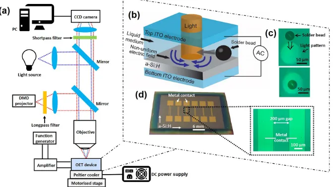
Fig. 1. (a) Schematic experimental setup. (b) 3D schematic of the OET device. (c) Microscope images of a solder microsphere attracted to the illuminated region under positive DEP force. (d) Image of the bottom OET electrode with six pairs of isolated metal contacts with different gaps. Inset: microscope image of the metal contacts with a 200µm gap.
2. Experimental setup and device structure
[image:4.612.143.480.217.406.2]sample of liquid medium and the solder beads. In the dark, the impedance of the a-Si:H layer is very high and the applied AC voltage is mainly dropped across this layer. However, when a light pattern is projected on to the a-Si:H layer, the impedance of this layer drops significantly, which makes the voltage drop predominantly across the liquid medium above the illuminated area, thus creating a non-uniform electric field between the dark and illuminated regions in the device chamber. This non-uniform electric field interacts with the samples in the liquid medium producing either attractive (positive DEP force) or repulsive (negative DEP force) depending on their Clausius-Mossotti (CM) factors [7]. Therefore, ‘traps’ can be created to manipulate the positions of samples in the OET device by controlling the positions of projected light patterns. For the solder microspheres used in this work, they were attracted to the illuminated regions under positive DEP force, as shown in Fig. 1(c).
Figure 1(d) shows the images of the bottom electrode of the OET device used in this work. Compared with conventional OET devices, this bottom electrode has six pairs of specifically-designed isolated metal contacts with different gaps (50µm, 100µm, 150µm, 200µm, 300µm, 400µm) on top of the a-Si:H layer. Such design is to demonstrate the use of OET to construct a microscale circuit via the assembly of solder microspheres to form electrical connections between the isolated metal contacts. The bottom OET electrode and top OET electrode were mounted together by a 150µm thick spacer to form a chamber, where the solution containing solder microspheres were injected via pipette. More information of the structure of the OET device and experimental details can be found in the Appendix.
3. Experiment and discussion
3.1. Parallel assembling, freezing-drying and heating solder microspheres
Fig. 2. Parallel assembling, freezing-drying and heating the solder beads. (a) Microscope image of the solder beads positioned at the edge of the metal contacts. (b) Microscope image of parallel assembly of solder beads to fill in the gap and form the straight line. (c) Straight line of solder beads formed by the light patterns. (d) Microscope image of formed straight line of solder beads after turning off the DMD projector. Videos showing the detailed assembling process of solder beads can be found inVisualization 1,Visualization 2. Microscope images of solder beads: (e) after assembling the solder beads, (f) after freezing the solder beads, (g) after sublimating the liquid medium, (h)after heating the solder beads. (i) SEM image of the assembled solder beads after heating. (j) SEM image of two adjacent solder beads before heating. (k) SEM image of two adjacent solder bead after heating.
and precise circuit construction. It is worth mentioning that OET has been demonstrated to be a compatible micromanipulation technology capable of assembling many different nano- and micro-scale objects, ranging from semiconductor nanowires and carbon nanotubes [17, 18], to metallic and dielectric particles on the order of tens of microns [10, 11, 20], to photonic/electronic devices with sizes greater than 100 microns [21, 22]. Additionally, alignment of particles with OET can be made as the assembly is ongoing in a way that would not be possible with either photo or e-beam lithography, giving added flexibility to the fabrication process. Therefore, we believe that OET has a great potential for micro-assembly applications on its own or together with other techniques, such as photolithography and 3D printing, if necessary.
structure between the adjacent solder beads is formed after the heating process. These SEM images provide clear evidence to show that the heating process melts the solder beads and makes the material on the surface of the bead flow toward the interfaces between the adjacent solder beads, forming the observed fused structure.
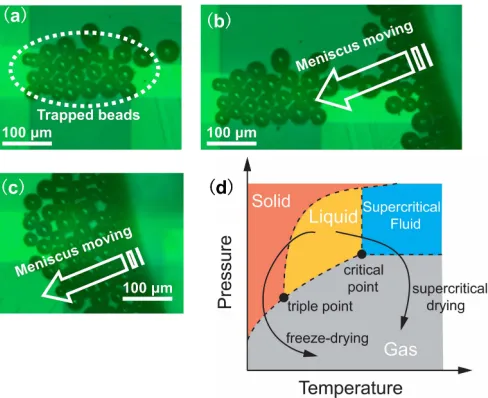
Fig. 3. (a) Trapped solder beads in OET device. (b)&(c) Trapped solder beads were dragged away by meniscus during the process of evaporating the solution. SeeVisualization 3for a video showing the detailed process. (d) Phase diagram of supercritical drying which goes beyond the critical point (high pressure/high temperature regime) and the freeze drying which goes below the triple point (low pressure/low temperature regime).
3.2. Freeze-drying
[image:7.612.185.429.153.352.2]supercritical drying producing good results [30]. Shown in Fig. 3(d) is the phase diagram of supercritical drying and freeze-drying, while both cases avoid the direct liquid-gas transition. Supercritical drying requires going from the liquid to the gas phase around the high pressure/high temperature side of the liquid’s critical point where the difference between liquid and gas become indistinct. By instead going from the liquid to the solid phase first and then to the gas phase, freeze-drying is easier to implement under a microscope in a typical micromanipulation setting and so this is the process that we developed. To freeze the liquid medium while avoiding moving the OET device, a Peltier cooler was coupled to the bottom of the OET device (see Fig. 1(a)). After the liquid medium was visibly frozen the OET device was put into a freezer (RS Biotech Eclipse 100) and kept at -80◦C for 10 minutes ensuring the completion of the freezing process. Then, the OET device was transferred to a freeze dryer (Thermo Heto PowerDry LL3000) to sublimate the frozen medium for 30 minutes. After the frozen medium was sublimated, the top ITO electrode of the OET device was removed to expose the assembled solder beads. During the experiment, it was found that a rapid freezing process can move the positions of the assembled solder beads and break the assembled pattern. Therefore, quantitative measurements were carried out to study the influence of freezing process on the finished structure.
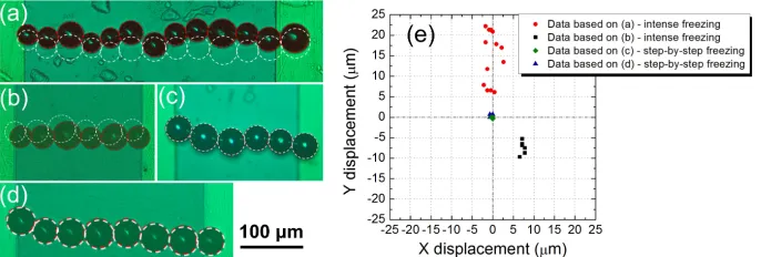
Fig. 4. Experimental results of the solder bead before freezing the solution and after sublimating the frozen medium. (a)-(d) Microscope images of the assembled solder beads before freezing the solution (outlined in white) and after sublimating the frozen medium (outlined in red) under different freezing conditions, in which rapid freezing was used for (a) and (b); step-by -step freezing was used for (c) and (d). Shown in (e) is the distribution of moving distances (in X-axis and Y-axis) of solder beads before freezing the solution and after sublimating the frozen medium. The moving distances are calculated based on the microscope images shown in (a)-(d).
20 microns whilst slowly freezing can keep the bead displacement to less than one micron. These results suggest that the freeze-drying method containing step-by-step freezing and sublimation can preserve the assembled microstructures of solder beads whist removing the liquid solution. Interestingly, under the rapid freezing process, the assembled solder beads didn’t move randomly from where they are placed; instead, they moved in a similar direction. This suggests that the movement is due to the crystallization process of the liquid medium, which starts at one side of the device and generates a force to move the beads at the interface between the solid phase (ice) and the liquid phase. For a free liquid droplet on a cold plate, the geometry of the freezing front results in a tip being formed on the frozen droplet [31]. However here we have two plates which the water freezes between producing a predominantly horizontal movement of the freezing front. The crystallization process tends to follow a specific direction pushing the beads along with it in horizontal plane (see Fig. 6(a)). In the step-by-step slow freezing process, the OET device may be cooled more uniformly allowing the crystallization process of the liquid to start at the bottom of the OET device and proceed vertically through the device inducing less horizontal freezing motion (see Fig. 6(b)). These results suggest the advantage of using freeze-drying to preserve fragile structures assembled by OET. More details of using freeze-drying to dry out MEMS structures and the advantage of reduced mechanical and thermal stresses were well described previously [30].
[image:9.612.149.470.324.434.2]Fig. 5. (a) Temperature profile of OET device with the Peltier cooler being driven at 3A for 10 minutes (quick freezing). (b) Temperature profile of OET device with the Peltier cooler being driven at 1 A for 2 minutes, 1.5 A for 2 minutes, 2 A for 2 minutes, 2.5 A for 3 minutes and 3 A for 5 minutes (step-by-step freezing).
[image:9.612.155.460.517.610.2]3.3. I-V measurement
[image:10.612.158.460.469.591.2]After assembling the solder beads and subsequently removing the liquid medium via freeze-drying, the OET device was placed on top of a hotplate (Cole-Parmer StableTemp) at 185◦C for five minutes to heat and melt the assembled solder beads (melting point 178◦C - 180◦C). The experimental results of assembling, freezing-drying and heating solder beads have been shown in Figs. 2(e)-(k). The current-voltage (I-V) characteristics of the isolated metal contacts connected by the solder beads were measured by a semiconductor device analyzer (Keysight B1500A) using a probe station (Casca-deMicrotech MPS150). As shown in Fig. 7(a), the resistances between the isolated metal contacts before and after assembling the solder beads (without heating) were measured to be around 108Ωand 107Ω, respectively. The drop of the resistance is due to the assembled solder beads, however, it is still very large. Figure 7(b) shows the I-V characteristic of the circuit after heating the assembled solder beads and the resistance was measured to be 11.6Ω. In this case, the assembled solder beads bridge an effective conductive path between the isolated metal contacts, inducing a significant drop of the resistance between the metal contacts. The SEM images show that the heating process melted the material from the surface of the solder beads and formed a fused structure between the adjacent solder beads, significantly reducing the interface resistance between them. The SEM images also show that the adjacent beads are fused together with a contact area over ten microns across. If the lithographically patterned contacts were connected by a single bar of solder tens microns in diameter over the 200 µm gap it is expected that the resistance of this bridge would be less than 1Ωaccording to the calculation shown in the Appendix. The fact that the bridge produced is more resistive than this suggests that the measured resistances are still dominated by the interfaces between beads and between the beads and the metal contacts even after the melting stage. Therefore, relevant work is currently on going to reduce the interface resistance by optimizing the heating process such as adjusting the temperature, time and sample’s ambient heating environment to create more conductive interfaces between the beads. Since the solder beads have a great potential to be used for creating electrical connections, our future work in this area will focus on using OET to assemble solder beads together with photonic and electronic components to make functional devices. A proof-of-concept demonstration of using OET to assemble solder beads and a micro-sized light-emitting diode (micro-LED) [32, 33] can be found in the Appendix.
Fig. 7. I-V characteristics. (a) I-V characteristics of the isolated metal contacts before and after assembling the solder beads (without heating). (b) I-V characteristic of the isolated metal contacts after heating the assembled solder beads.
4. Conclusion
techniques in a liquid environment. We have shown that by using a slow, step-by-step, freezing process micro solder beads can be preserved in a desired arrangement to within one micrometer of their initial positions whereas quickly freezing the solution can cause them to move by tens of microns. We further show that this level of control is sufficient to allow the subsequent fusing together of the solder beads by heating and melting them and that this fused connection has a relatively low resistance. Additionally, the OET device is capable of performing parallel manipulation of solder beads in the same plane, allowing the beads to be precisely assembled and interfaced with each other or other small electronic components which then is an enabling step towards manufacturing electrical circuits using OET rather than pick and place technologies. The freezing and subsequent freeze-drying process developed here however will be more generally applicable to other tweezing modalities such as optical, acoustic or magnetic tweezing allowing the preservation of patterned micro-particles for many applications.
5. Appendix
5.1. Sample preparation
The solder beads used in this work are commercially-available Sn62Pb36Ag2 microspheres (Industrie des Poudres Sphériques, France), which are in powder formats as provided from the company. To make the sample for the experiment, the beads were put into a solution, consisting of deionized water with 0.05% volume ratio of non-ionic surfactant TWEEN 20 (SIGMA P9416). Since the solder beads tend to ‘clump together’ in random complexes and stick onto the surface of pipette, adding TWEEN 20 in the solution can minimize the clumps and help transfer the beads into the OET device. The conductivity of the solution was measured to be 2 mSm−1after adding the TWEEN 20. To carry out the experiment, the solution containing the metallic microspheres was injected into the OET device at a volume of 10µL each time using a pipette and the device was biased with a 15 kHz 25 V peak-to-peak AC signal.
5.2. Device fabrication
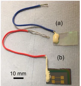
The OET device used in this work consists of a top electrode and a bottom electrode. The top electrode is made from a standard microscope glass slide (2.5 cm×7.5 cm×1mm) coated on one side with 600 nm thick ITO by magnetron sputtering (Diamond Coating Ltd, UK) (see Figs 8(a) and 8(b). To make the top electrode, the ITO-coated glass slide was cut to small pieces with sizes around 2.5 cm×1.5 cm using a diamond scriber. An electrical wire was bonded to the small piece of ITO-coated glass slide using a conductive silver paint (Agar Scientific, Acheson Silver DAG 1415M) and an epoxy resin (Mxbon Waterproof Epoxy-E41A). Image of the top electrode can be found in Fig. 9(a).
Fig. 8. (a)-(k) Step-by-step fabrication flow of the bottom OET electrode.
Fig. 9. Image of the OET device. (a) Image of the top OET electrode used in this work. (b) Image of the bottom OET electrode used in this work.
metal deposited on top of the photoresist. Therefore, specifically-designed metal contacts can be fabricated on top of the a-Si:H layer with SiO2insulation layer sandwiched in between (see Fig. 8(k)). To make the bottom electrode, the ITO-coated glass slide with a-Si:H layer and metal contacts was also cut to small pieces with sizes around 2.5 cm×1.5 cm. Then, a scratch knife was used to remove the a-Si:H at the edge to expose the conductive ITO layer, where an electrical wire was mounted using silver paint and epoxy as for the top electrode. An image of the bottom electrode can be found in Fig. 9(b). After the top and bottom electrodes were fabricated, they were attached together by a 150µm thick spacer to form a chamber, where the liquid medium containing the solder beads was injected via a pipette. This attached electrode pair formed the OET device used in this work.
5.3. Used equipment
[image:12.612.239.374.299.442.2]measure the temperature profiles of the OET device cooled by the Peltier.
5.4. Resistance calculation
A simplified model of solder bar (cylinder) was used to calculate the resistance of the bridge formed by the solder beads. For a single bar of solder with 10µm in diameter over the 200µm gap, it is expected that the resistance of this bar would be:
R=ρ·Lengt h
Ar ea =
ρ·l
π·r2 (1)
For the solder bead used in this work, the electrical resistivity (ρ) is 0.145Ω·µm;Lis 200µm; ris 5µm. Therefore, the resistance of the bar is calculated to be 0.4Ω.
Fig. 10. (a) Schematic of the micro-LED device. (b) Schematic layout of connecting solder beads to the metal contacts of a micro-LED device. (c) & (d) Microscope images of solder beads assembled by OET to connect with the metal contacts at the corners of the micro-LED device.
5.5. Assembling of the solder beads with the photonic device
Figure 10 shows the micro-assembly of solder beads to connect with the metal contacts of a micro-sized light-emitting diode (micro-LED) device using OET. The detailed device structure and fabrication procedures can be found in previously reported work [32, 33].
Funding
Engineering and Physical Sciences Research Council (EPSRC) (EP/L022257/1, EP/L00044X/1).
Acknowledgements
[image:13.612.185.438.244.454.2]