110GHz) was manufactured. Vector Network Analyser (VNA) measured return loss of the HOM coupler is shown to be < 10dB at 90 – 96 GHz. A transmission and phase measurement is presented to analyse TE61 mode conversion in the coupler.
Index Terms— Gyro-TWA, mode coupling, waveguide coupler, THz input coupler.
I. INTRODUCTION
Gyro-devices are sources of coherent EM radiation based on the cyclotron resonance maser (CRM) instability [1] capable of delivering high power microwave signals at THz frequencies. Applications of the gyro-devices include plasma heating [2], RADAR systems [3] and spectroscopes [4].
A W-band gyro-TWA has been developed at the University of Strathclyde for use on a cloud profiling RADAR system. The W-band device uses a three-fold helically corrugated interaction region (HCIR) [5]. The HCIR couples the TE21 mode to the first spatial harmonic of the TE11 mode [6] to generate an operating eigenwave, improving the instantaneous bandwidth [7]. A W-band gyrotron backward wave oscillator (gyro-BWO) with similar setup compared to the gyro-TWA achieved a maximum output power of 12 kW when driven by a 40 kV, 1.5 A, annular-shaped large-orbit electron beam [8]. The frequency tuning band of 88 – 102.5 GHz was achieved through cavity magnetic field adjustments.
A gyro-TWA operating at a centre frequency of 372 GHz is being studied for applications of Electron Paramagnetic Resonance (EPR) and Dynamic Nuclear Polarization (DNP) in a Nuclear Magnetic Resonance (NMR) system. High power, wide bandwidth (> 5%) gyro-amplifiers are ideal for pulsed EPR and DNP-NMR applications. If a 3-fold HCIR is used in the device, the mean radius is ~ 0.4 mm. Higher order mode (HOM) operation is proposed to increase the cavity dimensions and, hence, enhance the power handling capability of the waveguide cavity.
The gyro-TWA will require efficient coupling of the TE61 mode into the interaction cavity. Minimal power loss at the coupling interface will enable as much of the millimetre wave drive power to be available to the high efficiency interaction.
This work was supported by the Engineering and Physical Sciences Research Council (EPSRC) U.K. under Research Grant EP/K029746/1.
J. R. Garner ([email protected]), L. Zhang ([email protected]), C. R. Donaldson ([email protected]), A.W. Cross
([email protected]) and W. He ([email protected]) are with Department of Physics, SUPA, University of Strathclyde Glasgow, G4 0NG, Scotland.
input coupler is more complex than designing a fundamental mode coupler, due to the possibility of lower order mode (LOM) competition in the cavity. A TE11 field pattern is readily excited and is the dominant mode within a cylindrical waveguide. Therefore, to ensure high TE61 field purity, a complex waveguide coupling geometry is required.
The design of a power dividing input coupler for a 372 GHz HOM gyro-TWA is presented. The numerical modelling of a waveguide splitter input coupler with a linear taper power divider is presented in Section II. The linear taper and E-plane waveguide bend were simulated individually before the full design of the waveguide channel was completed. A tolerance study of the optimised waveguide coupler is discussed in Section III. A prototype waveguide coupler, scaled to operate at 90 – 96 GHz, was manufactured. A discussion of the coupler manufacture is included in Section IV and the Vector Network Analyser prototype testing is presented in Section V. Section VI discusses the design of the coupler at 93 GHz and 372 GHz.
II. 372 GHZ TAPERED WAVEGUIDE INPUT COUPLER The design of a 372 GHz TE10R – TE61C waveguide coupler employs the principal of incident wave power distribution to couple to a HOM [9]. The waveguide splitter divides an incident TE10 mode into equal signal intensities, propagating with matched phase towards the cylindrical coupled cavity. The possible modes which may be coupled into the interaction cavity are dependent on the number of branches employed within the designed waveguide splitter. A table of branch numbers and the relevant potential coupled modes, when equal length waveguide branches are used, is shown in Table I. By implementing the waveguide splitter, the generation of a HOM in the interaction cavity is simplified due to a reduction in mode competition.
The design of a waveguide TE61C input coupler can include a waveguide splitter with 2- or 3-branches (Table I). The 3-branch splitter would result in less mode competition inside the cylindrical cavity with a single lower order TEm1 mode propagating within the cavity (TE31); however, the phase matching of the 3 waveguide channels results in added complexity to the coupler design and manufacture. Therefore, a TE10R – TE61C input coupler with a 2-branch waveguide splitter was designed for a 360 – 384 GHz gyro-TWA.
Fig. 1: Schematic of a rectangular-to-square linearly tapered waveguide. linear or part-sinusoidal axial tapers with single E-plane variations [10], or double tapers which vary in the E- and H- plane simultaneously [11]. A linearly or sinusoidally tapered waveguide can be analytically examined using infinite step discontinuities [12]. A 372 GHz waveguide taper with a linear wall profile was designed for a rectangular-to-square (impedance ratio, Z = 2.00) waveguide transition.
TABLE I: WAVEGUIDE SPLITTER BRANCH NUMBER AND POTENTIAL MODES.
Branch No. Converting Mode Cavity TEmn Modes
2 TE21 TE21, TE41, TE61, …
3 TE31 TE31, TE61, TE91, …
4 TE41 TE41, TE81, TE12,1 …
5 TE51 TE51, TE10,1, …
A rectangular-to-square waveguide taper is shown in Fig. 1. The reflection coefficient (Γ) of a rectangular waveguide taper supporting TE10 mode propagation can be defined as [11];
(1)
where λg is the guide wavelength and L is the tapering section
length. K0, K1 and l are given by
(2)
(3)
Fig. 2: Simulated scattering of a 372 GHz rectangular-to-square waveguide taper.
(4)
respectively, where a and bdenote the waveguide width and height with the subscripts 0 and 1 representing the initial and final magnitudes respectively. A variation of a is only witnessed for a taper with an H-plane projection. For an E-plane rectangular-to-square taper where a0 = a1 and b1 = 2 ·b0,
equation (1) simplifies to
(5)
Analysis of equation (5) highlights a minimum reflection coefficient when L ≈ N · λg, where N is a whole integer number.
The guide wavelength at 372 GHz is ~ 1.10 mm; therefore, the taper length is set at N · 1.10 mm. To minimise wall losses, the taper length should be minimised. Therefore, N = 1.
A 372 GHz impedance matching tapered waveguide was designed using CST Microwave Studio (CST-MS). The waveguide width (a) was initially set at 0.60 mm with a waveguide width-to-height (a : b) ratio of 1 : 2. The taper length (L) was set at 1.10 mm. A parametric optimisation of a was performed to minimise reflections at the rectangular input port (Port 1). The numerically simulated transmission and reflection of a Z = 2.00 rectangular-to-square E-plane waveguide taper is shown in Fig. 2. The topology of the simulated waveguide taper is included in the inset. The waveguide width (a) was optimised at 0.570 mm, equating to b0 = 0.285 mm and b1 = 0.570 mm,
with the reflection at Port 1 less than -27 dB over the desired operating bandwidth. Therefore, the low reflection component may be used at the incident port.
An E-plane waveguide bend is a fundamental component of waveguide engineering. A rotation of a waveguide about an angle, commonly between 15° to 90°, creates a smooth-walled waveguide junction. The smooth E-plane transition can be designed to be compact (small RIN) or broad (large RIN) with
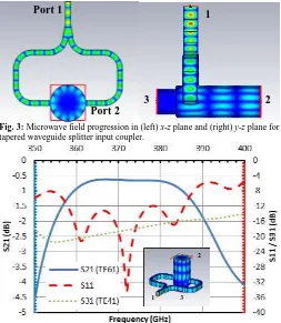
[image:2.612.51.275.51.211.2] [image:2.612.75.298.552.695.2]to the TE61 mode, a small taper may be employed between the input coupler and the cavity to permit maximum coupling into the interaction cavity. Therefore, R can be varied within 1.00 (cut-off radius of TE61 at 360 GHz) to 1.40 mm to support the desired TE61 mode and, hence, optimisation of R may be carried out on the HOM input coupler. The beam tunnel is coupled to the rectangular input port from two discrete waveguide branches which consist of 3 E-plane bends adjoined to the tapered waveguide transition. The two waveguide branches evenly split the signal from the input port (Port 1), propagating the divided wave in the ± x-direction before propagating the two synchronous signals into the beam cavity. The 2D progression of the mm-wave propagation is shown in Fig. 3. Fig. 3 (left) highlights coupling to the TE61C mode for an optimised cavity radius (R) of 1.03 mm. The generated HOM will be able to freely propagate towards the cavity and the diode region unless Port 3, the port defined as being adjacent to the electron gun, is terminated. The average electron beam radius (RB)from the electron gun is 0.20 mm [13]; therefore, due to the
HOM cavity a cut-off waveguide (Fig. 3 (right)) may be employed to prevent the propagation of incident radiation into the diode, without intercepting the electron beam. A parametric optimisation of RC is performed with a range of (0.70 – 0.85)
mm to cut-off all modes higher in frequency than the TE41 mode whilst ensuring a large beam tunnel diameter.
Fig. 4 highlights the 372 GHz TE10R – TE61C tapered waveguide splitter input coupler operating between 359 – 385 GHz. The 3D E-field progression on the conductor walls is shown in the inset with port numbers defined. The bandwidth of the input coupler equates to ~ 7%. The cut-off waveguide reflector (RC = 0.80 mm) is effective at preventing significant
wave power from propagating towards the electron gun with a signal level of < -15 dB for the dominant TE41 mode. The distance between the near edge of the rectangular waveguide branches and the waveguide reflector (L1) is 0.272 mm. The
coupler shows a high TE61 mode selectivity performance with low magnitude coupling to subsequent LOM’s and HOM’s. A gyrating electron beam will occupy ~ 25% of the cut-off reflector cross-sectional area; hence, the potential of electron bombardment on the cavity boundaries is minimal and an increased beam diameter may be employed. Return loss at the input port (Port 1) is < 12 dB over the operating bandwidth of 360 – 384 GHz.
At 372 GHz, the skin depth of a mm-wave signal in a copper waveguide is ~ 0.1 µm. Hence, the depth at which the signal propagates within the waveguide wall is comparable to, or smaller than, the surface roughness. Therefore, Ohmic losses
Fig. 4: Numerical scattering of a TE10 – TE61 tapered waveguide splitter input coupler.
will increase with an uneven waveguide finish. With consideration of the surface effects on electrical conductivity, a reduction factor was applied to the copper conductivity (0.5x10⁷ Sm-1). The coupling strength at 372 GHz, numerically simulated with CST-MS, was shown to decrease by 0.91 dB with a coupling strength of -0.77 dB for a perfect electrical conductor (PEC) background material and -1.68 dB for a reduced conductivity copper background. A smooth surface finish (Ra = 2 – 3 µm) must be achieved in manufacture to
ensure a high TE61 coupling factor.
III. TOLERANCE STUDY
A tolerance study was performed on the 372 GHz tapered waveguide input coupler to test the feasibility of the coupler performance with parametric discrepancies resulting from fabrication tolerances. Initially, the rectangular splitter waveguide is analysed. The parameters which govern the waveguide dimensions (a, b, L and RIN) were varied from the
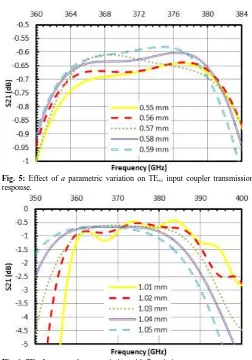
optimum value to test the tolerance range over which the coupler may operate. A plot of waveguide width variation (a) for fixed values of b and L is shown in Fig. 5.
The resultant change to the transmission coefficient for a = ± 20 µm highlights an operational frequency shift of ~ 0.5 GHz for a 10 µm variation. A frequency shift of 0.5 GHz magnitude would not affect the coupler operation at 360 – 384 GHz; however, larger magnitude a discrepancies would result in a frequency shift that was out with the desired bandwidth. The waveguide height (b) was varied for fixed a and L. The investigation highlighted minimal frequency or coupling strength response for Δb = ± 20 µm; therefore, the waveguide height has no strict tolerance requirement. The taper length (L) is subsequently varied with no detrimental effects on coupling
1 3
[image:3.612.314.567.49.340.2]Fig. 5: Effect of a parametric variation on TE61 input coupler transmission response.
Fig. 6: TE61Input coupler transmission with R variations.
performance for ΔL ± 25 µm. The waveguide bend radius (RIN)
was investigated with optimum values of a, b and L. For ΔRIN
values of ± 100 µm, no effect on coupling strength or frequency response was observed. However, an RIN increase will result in
enhanced waveguide losses due to an increase in propagation length. The coupler performance as a result of rectangular waveguide discrepancies remains broadly unaffected.
An investigation into the coupled cavity is subsequently performed for R and L1. The cavity radius (R) should be
carefully manufactured to ensure a tight tolerance. Fig. 6 shows the effect of up to ΔR = ± 20 µm on the tapered input coupler performance. The effect of R variations is shown to have a significant effect on the coupler centre frequency with a 10 µm discrepancy in R resulting in a 3 GHz shift. Hence, the machining of R must be very precise.
A review of the L1 parameter was performed (Fig. 7).
Alterations resulting in 25 µm increases to L1 are shown to
decrease the centre frequency by ~ 2 GHz. The discrepancies to
L1, which result in a phase mismatch between the incident and
reflected wave at Port 3, is shown to affect the coupler bandwidth and coupling strength with deviation from the optimum.
IV. INPUT COUPLER MANUFACTURE
[image:4.612.316.560.48.216.2]A W-band prototype TE61 tapered-waveguide input coupler was manufactured to confirm the simulated reflection results. The coupler was scaled to operate at 90 – 96 GHz due to limitations on achievable tolerances using in-house
Fig. 7: Effect of L1 variation on input coupler transmission response.
manufacture. The circular coupled waveguide was scaled directly with a 4x dimension increase on the 372 GHz design. The rectangular input waveguide was designed to maintain the aspect ratio used in the 372 GHz design between standard WR2.2 (a’ x b’) waveguide and a0x b0. A tapered section from
standard W-band waveguide to the optimised coupler waveguide is included in the scaled design.
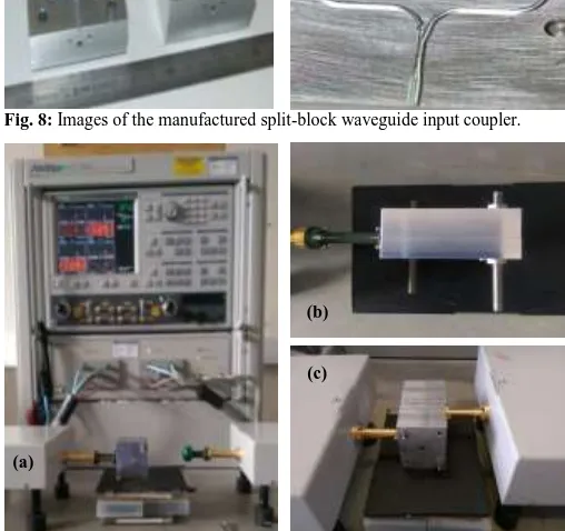
The aluminium block was split into two discrete sections. A waveguide channel was manufactured into each split-block using a 3-axis Computer Numerically Controlled (CNC) milling technique. The tool path was machined into each split-block using a 0.60 mm end mill with half the waveguide channel width (1.27 mm depth) milled into each aluminium block. The length of the end mill cutter would prohibit the machining of the full waveguide width into a single block. The circular waveguide and waveguide reflector radii (R = 4.10 mm and Rc = 3.20 mm) were subsequently drilled. A flange
connection was machined into the split-block coupler to allow for direct attachment to the VNA. A series of threaded rods were used to join the split-block structure to prevent any loss of signal between the block faces. The manufactured waveguide channel is shown in Fig. 8.
[image:4.612.49.296.51.209.2]V. VECTOR NETWORK ANALYSER TESTING TABLE II: WAVEGUIDE COUPLER DIMENSION COMPARISON
Parameter 372 GHz Design (mm)
93 GHz Design (mm)
93 GHz Actual (mm)
R 1.030 4.10 4.12
RC 0.800 3.20 3.45
a0 0.570 2.60 2.60
a’ 0.560 2.54 2.60
b0 0.235 0.95 0.90
b’ 0.280 1.27 1.23
b1 0.570 1.90 1.80
RIN 0.800 2.72 2.75
ROUT 1.085 3.67 3.65
L1 0.272 1.10 1.17
[image:4.612.309.571.514.693.2]Fig. 9: VNA measurement setup with 2- and 4- block coupler.
Images of the coupler split-block attached to the VNA are shown in Fig. 9(a)-(b).
A comparison of the prototype 94 GHz and 372 GHz waveguide coupler dimensions is shown in Table II. A discrepancy between the designed and manufactured parameter sets was highlighted with precision measurement of the manufactured waveguide channel using a travelling microscope. The manufactured parameter set is included in Table II. A comparison of the 90 – 96 GHz waveguide coupler numerical scattering with the designed and actual parameter set is shown in Fig. 10. The parametric discrepancies are shown to down shift the operating frequency range of the W-band tapered waveguide coupler.
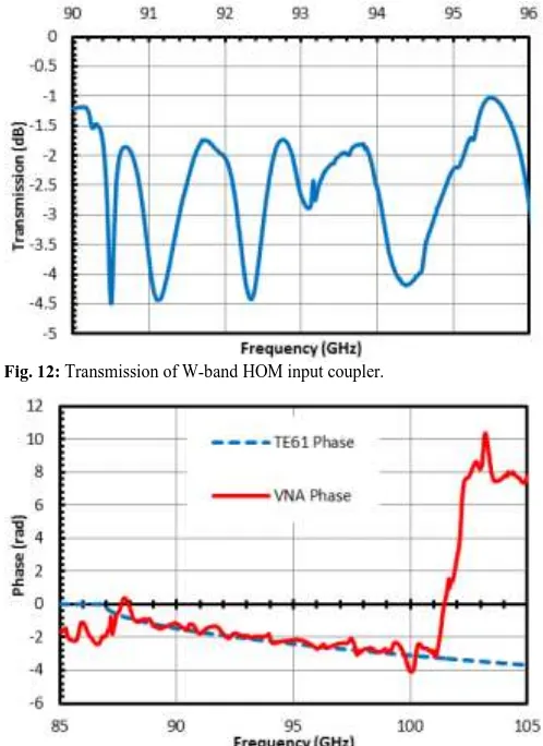
The HOM coupler numerical reflection for the designed and actual parameter set and VNA reflection results are shown in Fig. 11. Fig. 11 shows that the measured VNA reflection from the rectangular input port (Port 1) is in good agreement with CST-MS simulation results when open boundaries replace waveguide ports at Port 2 and Port 3. The S11 reflection at the input port is < - 10 dB between 90 – 96 GHz; therefore, > 90% of incident radiation is propagated into the coupled waveguide. A reciprocal waveguide coupler was manufactured to allow for transmission and phase measurement. Therefore, the waveguide mode can be evaluated. The 4 block experimental setup is shown in Fig. 9(c). The transmission of two identical waveguide couplers back-to-back is shown in Fig. 12. The average transmission loss is ~ 3dB equating to an individual coupler loss of -1.5 dB. The circuit loss in an individual aluminium coupler block was measured at -1 dB; therefore, high mode conversion is exhibited by the HOM waveguide coupler.
To confirm the mode of conversion, an additional waveguide section of length 3.00 mm was manufactured and inserted
Fig. 10: Simulated transmission and reflection of W-band split block coupler for design and manufactured parameter sets.
Fig. 11: Comparison of CST-MS and VNA coupler reflection results. between the two couplers to measure the phase response. The measured phase was then compared with the theoretical phase response of the TE61 mode in a waveguide of radius R = 4.10 mm. The theoretical and measured phase is shown in Fig. 12. The phase measurement has close correlation to the theoretical TE61 phase at 88 – 98 GHz; therefore, the waveguide coupler is shown to have a high TE61 mode conversion efficiency. The insertion loss (< 10 dB) and phase measurements suggest > 90% transmission to the TE61 mode.
VI. DISCUSSION AND CONCLUSION
The design of a 372 GHz TE10R – TE61C input coupler for a gyro-TWA has been presented. The design of the HOM input coupler focussed upon achieving a broadband coupling with a high transmission coefficient whilst ensuring the TE61 mode was dominant within the coupled cavity. The tapered waveguide input coupler was designed with low loss rectangular waveguide components. The tapered waveguide was shown to have a return loss of < 27 dB. The incident split signal was coupled into a circular waveguide through smooth walled E-plane waveguide bends. The waveguide bends had a reflection coefficient of < -40 dB over the 360 – 384 GHz operating bandwidth. The tapered waveguide input coupler achieved an operating bandwidth of 7% (359 GHz – 385 GHz). A tolerance study of the TE10R – TE61C tapered waveguide input coupler was performed to analyse the effect of manufacturing discrepancies on the coupler performance. The coupler was shown to be stable with manufacturing
(a)
[image:5.612.313.563.101.388.2] [image:5.612.45.299.109.348.2]Fig. 12: Transmission of W-band HOM input coupler.
Fig. 13: Theoretical and numerical dispersion of TE61 mode in coupler. discrepancies associated to the rectangular splitter waveguide. A maximum coupling change of 0.1 dB was observed for 20 µm variations of a corresponding to a frequency shift of ~ 0.5 GHz. An investigation into the coupled cylindrical beam tunnel, however, highlighted a frequency and coupling strength sensitivity with R and L1 variations. For ΔR = ± 10 µm, a 3 GHz
centre frequency shift was observed and for ΔL1 = ± 25 µm the
centre frequency was shifted by ~ 2 GHz. A decrease in coupling strength was also associated with R and L1
discrepancies (Fig. 6 and Fig. 7). Therefore, to ensure high coupling over the desired 360 – 384 GHz bandwidth the beam tunnel must be accurately manufactured with strict tolerances applied.
A W-band TE61 prototype coupler was manufactured to allow for VNA testing of the tapered waveguide input coupler. A CNC milling technique was used to machine a waveguide channel designed to operate at 90 – 96 GHz. The waveguide dimensions were scaled from the optimised 360 – 384 GHz TE10R – TE61C tapered waveguide input coupler. The 2-piece aluminium split block coupler design allowed for VNA testing of the coupler reflection. The measured S11 reflection from the input rectangular port (Port 1) of the coupler structure was shown to be < -10 dB between 90 – 96 GHz. The VNA measurement agreed well with simulated data, suggesting ~ 90% of incident radiation is transmitted into the circular coupled waveguide. A transmission and phase measurement with a reciprocal input coupler was presented. The phase difference analysis permitted the determination of the TE61 conversion into the coupled waveguide with the measurement
shown to be in good agreement with theoretical TE61 phase over the operating bandwidth.
The manufacturing technique outlined for the W-band HOM input coupler may be used in the manufacture of a 372 GHz waveguide coupler; however, state-of-the-art micro-milling technology must be employed. High precision laboratories [14] have the capability to machine waveguide channels of 0.1 mm width with a positional accuracy of ± 0.3 µm using 5-axis micro-milling machines and an appropriate end-mill tool piece. A surface finish with Ra = ~ 2 µm would ensure that Ohmic
losses would be minimised. Therefore, the design of a HOM power splitting waveguide coupler with waveguide sub-mm a x
b cross-section (0.57 x 0.24 mm) is realistic. VII. REFERENCES
1. K. R. Chu, “The electron cyclotron maser,” Rev. Mod. Phys. vol. 76, no. 2, pp. 489-540, 2004.
2. S. Coda et al., “Electron cyclotron current drive and suprathermal electron dynamics in the TCV tokamak,” Nucl. Fusion, vol. 43, no. 11, pp. 1361 – 1370, 2003.
3. M. G. Czerwinski and J. M Usoff, “Development of the Haystack Ultrawideband Satellite Imaging Radar,” Linc. Lab. J., vol. 21, no. 1, pp. 28 - 44, 2014.
4. E. A. Nanni et al., “THz Dynamic Nuclear Polarization NMR,” IEEE THz Sci. Techn., vol. 1, no. 1, pp. 145 – 163, 2011.
5. L. Zhang et al., “Multi-mode coupling wave theory for helically corrugated waveguide,” IEEE Trans. Microw. Theory Techn. vol. 60, pp. 1-7, 2012. 6. L. Zhang et al., "Design and Measurement of a Broadband Sidewall Coupler
for a W-Band Gyro-TWA", IEEE Trans. Microw. Theory Tech., vol. 63, pp. 3183-3190, 2015.
7. V. L. Bratman et al., ‘High-gain wide-band gyro-travelling wave amplifier with a helically corrugated waveguide’, Phys. Rev. Lett., vol. 84, pp. 2746-2749, 2000.
8. W. He et al., “High power wideband gyrotron backward wave oscillator operating towards the terahertz region,” Phys. Rev. Lett. vol. 110, pp. 165101, 2013.
9. C. F. Yu and T. H. Chang, "High-performance circular TE01-mode converter," IEEE Transactions on Microwave Theory and Techniques, vol. 53, no. 12, pp. 3794-3798, 2005.
10.K. Matsumaru, “Reflection coefficient of E-plane tapered waveguides,”
IRE Trans. Microw. Theory Techn. vol. 6, no. 2, pp. 143 – 149, 1958.
11.R. C. Johnson, “Design of linear double tapers in rectangular waveguide,”
IRE Trans. Microw. Theory Techn. vol. 7, no. 3, pp. 374 – 378, 1959.
12.R. A. Waldron, “Theory of reflections in a tapered waveguide,” J. I. Electron. Rad. Eng. vol. 32, no. 4, pp. 245 – 254, 1966.
13.J. R. Garner et al., “Design Study of a Fundamental Mode Input Coupler for a 372-GHz Gyro-TWA I: Rectangular-to-Circular Coupling Methods,”
IEEE Trans. Electron Devices, vol. 63, no. 1, pp. 497 - 503, 2016.
14.Science and Technology Facilities Council, “CNC Nano-machining,”
![Fig. 1: Schematic of a rectangular-to-square linearly tapered waveguide. linear or part-sinusoidal axial tapers with single E-plane variations [10], or double tapers which vary in the E- and H- plane simultaneously [11]](https://thumb-us.123doks.com/thumbv2/123dok_us/1525385.105109/2.612.75.298.552.695/schematic-rectangular-linearly-tapered-waveguide-sinusoidal-variations-simultaneously.webp)