Scalable Quantum Photonics with Single Color
Centers in Silicon Carbide
Marina Radulaski*†, Matthias Widmann*§, Matthias Niethammer§, Jingyuan Linda Zhang†, Sang-Yun Lee§∂, Torsten Rendler§, Konstantinos G. Lagoudakis†, Nguyen Tien Son‡, Erik Janzén‡, Takeshi Ohshima÷, Jörg Wrachtrup§, Jelena Vučković †
† E. L. Ginzton Laboratory, Stanford University, Stanford, California 94305, United States
§ 3rd Institute of Physics, IQST and Research Center SCOPE, University of Stuttgart, 70569 Stuttgart, Germany
∂ Center for Quantum Information, Korea Institute of Science and Technology (KIST), Seoul,
02792, Republic of Korea
‡ Department of Physics, Chemistry and Biology, Linköping University, SE-58183 Linköping,
Sweden
ABSTRACT
Silicon carbide is a promising platform for single photon sources, quantum bits (qubits) and nanoscale sensors based on individual color centers. Towards this goal, we develop a scalable array of nanopillars incorporating single silicon vacancy centers in 4H-SiC, readily available for efficient interfacing with free-space objective and lensed-fibers. A commercially obtained substrate is irradiated with 2 MeV electron beams to create vacancies. Subsequent lithographic process forms 800 nm tall nanopillars with 400-1,400 nm diameters. We obtain high collection efficiency, up to 22 kcounts/s optical saturation rates from a single silicon vacancy center, while preserving the single photon emission and the optically induced electron-spin polarization properties. Our study demonstrates silicon carbide as a readily available platform for scalable quantum photonics architecture relying on single photon sources and qubits.
KEYWORDS: color centers, silicon carbide, photonics, spintronics, nanopillars, spin-qubits.
Silicon carbide (SiC) has recently emerged as a host of color centers with exceptional brightness1 and long spin coherence times,2-5 much needed for the implementations of solid-state quantum bits and nanoscale magnetic sensors.6 In addition to a favorable set of physical properties, such as the wide band gap and high index of refraction, this material also benefits from the decades of utilization in power electronics7 – wafer scale substrates are available for purchase, doping and various etching processes8-11 are at an engineer’s disposal. This makes SiC advantageous over diamond and rare-earth doped crystals for industrial applications in quantum computing and sensing, as well as for integration of point defects with electronics and CMOS devices. Electron spins of various SiC color center ensembles have been coherently controlled to date.3,12,13 We focus our attention on individual silicon vacancy (VSi) centers in 4H-SiC, whose electron spin was recently employed as room temperature qubit,2 the first one at the single defect level in SiC. This system features spin coherence times of at least 160 µs, and with a potential for improvement through isotopic purification. To bring this system closer to the applications, we address VSi/4H-SiC platform from the points of scalability, device footprint, optical interface and collection efficiency, while preserving optically induced electron-spin polarization properties.
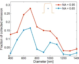
array of color center sites.15 Both of these approaches relied on collection into high numerical aperture (NA = 1.3) oil immersion lens, in a direct contact with the substrate. Vertically directed waveguiding in nanopillars allowed us to observe up to 22 kcounts/s (kcps) collection from single color centers with half the NA value. This is comparable to the best previous result of 40 kcps achieved in a non-scalable system,2 and a threefold increase over 7 kcps result in a scalable array in bulk.15 The use of NA = 0.95 air objective lens would result in a few-fold increase in collection efficiency, as discussed in Supporting Information. We also observe 2-4% relative intensity in optically detected magnetic resonance (ODMR), comparable to the previous result.2 Finally, the preservation of optical and spin properties of VSi centers makes this platform applicable for wafer-scale arrays of single photon sources and spin-qubits.
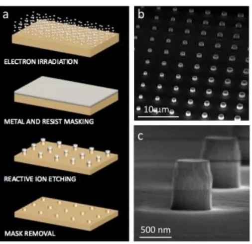
Fabrication. We develop a scalable nanofabrication process, based on electron irradiation and electron beam lithography, which produces tens of thousands of nanopillars per squared millimeter in 4H-SiC substrate that incorporates VSi color centers. Fig. 1a illustrates the process flow. The initial sample is a commercially available high purity semi-insulating 4H-SiC crystal, irradiated with 2 MeV electrons at a fluence of 1014 cm-2 at room temperature. For the purposes of hard etch mask, 300 nm of aluminum was evaporatively deposited onto the sample. Microposit ma-N negative tone resist was spun over it for patterning of nanopillars in 100 keV JEOL (JBX-6300-FS) electron beam lithographic system. Aluminum hard mask was etched in Cl2 and BCl3 plasma, and the pattern was transferred to silicon carbide in an SF6 plasma process, both performed in the Versaline LL-ICP Metal Etcher. The mask was stripped in KMG Aluminum Etch 80:3:15 NP.
shape of a cone frustum, reducing the top diameter by 120 nm. Fig. 1b-c show the SEM images of the fabricated structures.
Collection efficiency. We model emission of color centers placed in pillars using Finite-Difference Time-Domain method. Index of refraction distribution is made according to the profile of fabricated pillars (nSiC = 2.6, nair = 1) and continuous wave dipole excitation at 918 nm is positioned within. We consider nanopillars of 400 – 1,400 nm diameter with excitation at the central axis of the pillar (r = 0, z = 400 nm) with in-plane (Er) and vertically oriented (Ez) dipole components. The orientation of VSi dipole in our samples is along main crystal axis which forms 𝜃 = 4° angle with z-axis, and therefore we add the components to obtain total collected field 𝐸 =
Single photon emission. Photoluminescence (PL) measurements obtained in a home-built confocal microscope at room temperature are shown in Fig. 3. Light from a single-mode laser diode operating at 730 nm was sent to an air objective (Zeiss Plan-Achromat, 40x/0.65 NA), in order to excite the defects. The PL signal was collected with the same objective and sent through a dichroic mirror and subsequently spatially filtered by a 50 µm diameter pinhole. The photons emitted by the defects were spectrally filtered by a 905 nm long pass filter and finally collected with two single photon counting modules in a Hanburry-Brown-Twiss configuration, or, alternatively, with a spectrometer (details presented in Supporting Information). The density of color centers is too high to resolve single defects in the bulk crystals with no fabricated structures, however, combined with the nanopillars, a spatial separation of single defects is possible, simultaneously providing a moderate yield of defects placed in the pillars, as shown in Fig 3a. Approximately 4 out of 100 pillars host single VSi defects which desirable lateral and vertical placement, and show an enhanced photon count-rate compared to defects without photonic structure15. For each investigated VSi defect a laser power dependent saturation curve of the PL was collected as shown in Fig. 3b. The background was obtained by collecting the light from an empty pillar nearby and subtracted from the defects emission. The influence of the diameter was experimentally examined by a statistical analysis of the maximum PL intensity as a function of the diameter. The maximum PL was obtained by fitting the background-corrected saturation curve with a power law: 𝐼(𝑃) = 𝐼𝑠
1+𝛼/𝑃 , where I is the PL intensity as a function of the excitation power
diameter, showing 𝐼𝑚𝑎𝑥 = 22 kcps, which is an increase of factor of 2-3 compared to 5-10 kcps for a single VSi defect without photonic structures reported in literature2,15,16. This increase is smaller than expected from the model, which is attributed to the imperfect fabrication profile. A typical room temperature PL spectrum is shown in Fig. 3d, while Fig. 3e shows a typical second order autocorrelation measurement with a clear single photon emission characteristic.
observed, also in other samples17 but the further investigation of the origin is not in the scope of this work. The relative intensity of ODMR was calculated as (𝑃𝐿𝑜𝑛− 𝑃𝐿𝑜𝑓𝑓 )/𝑃𝐿𝑜𝑓𝑓 and it varies between 2%-4%, which is in good agreement with previous single spin studies.2,15
beam irradiation can be applied to each fabricated nanopillar to generate color centers at a desired location, as has been recently demonstrated in diamond systems.29
Figure 3. a) Photoluminescence intensity map of a block of pillars. b) PL intensity of a single VSi as a function of the optical power, saturating at 22 kcps. The red line shows a fit to the data. c) Diameter dependent collected count rate. d) Typical room temperature PL spectrum of a single VSi emitter in a nanopillar. e) Typical second order correlation function showing anti-bunching at zero time delay, a clear evidence for single photon emission. The red line shows a double exponential fit to the data (details in Supporting information). f) ODMR signal from a single VSi in a nanopillar. The red line shows a Lorentzian fit to the data.
AUTHOR INFORMATION
Corresponding Author
* marina.radulaski@stanford.edu
Author Contributions
All authors have given approval to the final version of the manuscript. *These authors contributed equally.
Funding Sources
This work is supported by the National Science Foundation DMR Grant Number 1406028, by
the Army Research Office under contract W911NF1310309, by the German Federal Ministry of Education and Research (BMBF) through the ERA.Net RUS Plus Project DIABASE, and by the JSPS KAKENHI (B) 26286047.
Notes
The authors declare no competing financial interest.
REFERENCES
(1) Castelletto, S.; Johnson, B. C.; Ivady, V.; Stavrias, N.; Umeda, T.; Gali, A.; Ohshima, T. Nat. Mater. 2014, 13, 151-156.
(2) Widmann, M.; Lee, S. Y.; Rendler, T.; Son. N. T.; Fedder, H.; Paik, S.; Yang, L.P.; Zhao, N.; Yang, S.; Booker, I; Denisenko, A.; Jamal, M.; Momenzadeh, S. Al.; Gerhardt, I.; Ohshima, T.; Gali, A.; Janzen, E.; Wrachtrup, J. Nat. Mater. 2015, 14, 164-168.
(3) Seo, H.; Falk, A. L.; Klimov, P. V.; Miao, K. C.; Galli, G.; Awschalom, D. D. Nature
Commun., 2016, 7.
(4) Yang, L.P.; Burk, C.; Widmann, M.; Lee, S.Y.; Wrachtrup, J.; Zhao, N., Phys. Rev. B
2014, 90(24), p.241203.
(5) Christle, D. J.; Falk, A. L.; Andrich, P.; Klimov, P. V.; Hassan, J. U.; Son, N. T.; Janzén,
E.; Ohshima, T.; Awschalom, D. D. Nat. Mater. 2015, 14(2), pp.160-163.
(6) Kraus, H.; Soltamov, V. A.; Fuchs, F.; Simin, D.; Sperlich, A.; Baranov, P. G.; Astakhov, G. V.; Dyakonov, V. Sci. Rep. 2014, 4, 5303.
(7) Casady, J. B.; Johnson R. W. Solid State Electron. 1996, 39, 10, 1409-1422.
(8) Radulaski, M.; Babinec, T. M.; Buckley, S.; Rundquist, A.; Provine, J.; Alassaad, K.; Ferro, G.; Vučković, J. Opt. Express 2013, 21(26), 32623-32629.
(9) Radulaski, M.; Babinec, T. M.; Müller, K.; Lagoudakis, K. G.; Zhang, J.L.; Buckley, S.; Kelaita, Y. A.; Alassaad, K.; Ferro, G; Vučković, J. ACS Photonics 2014, 2, 14-19.
(10) Magyar, A. P.; Bracher, D.; Lee, J. C.; Aharonovich, I.; Hu, E. L. Appl. Phys. Lett. 2014, 104, 5, 051109.
(11) Song, B. S.; Yamada, S.; Asano, T.; Noda, S. Opt. Express 2011, 19(12), 11084-11089.
(12) Falk, A. L.; Buckley, B. B.; Calusine, G.; Koehl, W. F.; Dobrovitski, V. V.; Politi, A.;
(13) Mizuochi, N.; Yamasaki, S.; Takizawa, H.; Morishita, N.; Ohshima, T.; Itoh, H.; Isoya, J. Phys. Rev. B 2002, 66(23), p.235202.
(14) Kato, S.; Chonan, S.; Aoki, T. Opt. Lett. 2014, 39(4), 773-776.
(15) Wang, J.; Zhou, Y.; Zhang, X.; Liu, F.; Li, Y.; Li, K.; Liu, Z.; Wang, G.; Gao, W. arXiv.org
2016, 1610.03978.
(16) Fuchs, F.; Stender, B.; Trupke, M.; Simin, D.; Pflaum, J.; Dyakonov, V.; Astakhov, G.V.
Nat. Commun. 2015, 6, 7578.
(17) Sörman, E.; Son, N. T.; Chen, W. M.; Kordina, O.; Hallin, C.; Janzén, E. Phys. Rev. B
2000, 61, 2613.
(18) Janzén, E.; Gali, A.; Carlsson, P.; Gällström, A.; Magnusson, B.; Son, N.T. Physica B:
Condens. Matter 2009, 404(22), pp. 4354-4358.
(19) Niethammer, M.; Widmann M.; Lee, S-Y.; Stenberg, P.; Kordina, O.; Ohshima, T.; Son, N. T.; Janzén, E.; Wrachtrup, J. Phys. Rev. Appl. 2016, 6, 3, 034001.
(20) Lee, S. Y.; Niethammer, M.; Wrachtrup, J. Phys. Rev. B 2015, 92(11), 115201.
(21) Lohrmann, A.; Iwamoto, N.; Bodrog, Z.; Castelletto, S.; Ohshima, T.; Karle, T.J.; Gali,
A.; Prawer, S.; McCallum, J.C.; Johnson, B.C. Nat. Commun. 2015, 6, 7783.
(22) Lienhard, B.; Schröder, T.; Mouradian, S.; Dolde, F.; Tran, T.T.; Aharonovich, I.;
Englund, D.R. Optica 2016, 3, 768–774.
(23) Saddow, S. E. Silicon carbide biotechnology: a biocompatible semiconductor for advanced biomedical devices and applications. Elsevier, 2012.
(24) Simin, D.; Soltamov, V.A.; Poshakinskiy, A.V.; Anisimov, A.N.; Babunts, R.A.;
Tolmachev, D.O.; Mokhov, E.N.; Trupke, M.; Tarasenko, S.A.; Sperlich, A.; Baranov,
P.G. Phys. Rev. X. 2016, 6, 31014.
(25) Soykal, Ö. O.; Dev, P.; Economou, S. E. Phys. Rev. B 2016, 93(8), 081207.
(26) Baranov, P.G.; Bundakova, A.P.; Soltamova, A.A.; Orlinskii, S.B.; Borovykh, I.V.; Zondervan, R.; Verberk, R.; Schmidt, J. Phys. Rev. B 2011, 83(12), 125203.
(27) Babinec, T.M.; Hausmann, B.J.; Khan, M.; Zhang, Y.; Maze, J.R.; Hemmer, P.R.;
Lončar, M., Nat. Nanotechnol. 2010, 5(3), pp.195-199.
(28) Ohno, K.; Joseph Heremans, F.; Bassett, L.C.; Myers, B.A.; Toyli, D.M.; Bleszynski Jayich, A.C.; Palmstrøm, C.J.; Awschalom, D.D., Appl. Phys. Lett. 2012, 101, p.082413.
(29) Schröder, T.; Trusheim, M.E.; Walsh, M.; Li, L.; Zheng, J.; Schukraft, M.; Pacheco, J.L.;
Camacho, R.M.; Bielejec, E.S.; Sipahigil, A.; Evans, R.E., arXiv.org 2016, 1610.09492.
SUPPORTING INFORMATION
S1a shows that the collection is highest when the color center is placed in the bottom half of the pillar. This result can have practical implications to the depth of ion irradiation induced color centers in future approaches. Fig. S1b shows that the collection is highest close to the central axis of the pillar, which can be applied for masked irradiation which would target central positions along pillar diameter.
Figure S1. a) Collection efficiency dependence on vertical position along the central axis (r = 0), where negative values correspond to the top of the nanopillar, and positive ones to the bottom, plotted for various diameters. b) Collection efficiency dependence on horizontal position along the radius at the central heights (h = 400 nm), plotted for various diameters.
Figure S2. Collection efficiency from VSi at the center of the nanopillar (r = 0, h = 400 nm) into air objective with NA = 0.65 and NA = 0.95.
Figure S3. a) SEM image of a pattern with nanopillars and unetched bulk regions. b) Photoluminescence measurements at T = 7 K, showing same linewidth for nanopillars as in the bulk unetched region, as well as the increased collection efficiency.
[image:16.612.74.556.425.593.2]Optical characterization of the sample is performed in the home-built confocal microscope shown in Fig. S4. A single mode laser (Openext) operating at 730 nm is sent over a dichroic mirror towards the objective (Zeiss, Plano-Achromat 40x/0.65NA), where it is focused onto the sample. The objective is mounted on a piezo-electric stage with a travel range in x-y-z of (100 100 10) µm, respectively. Fluorescence from the emitters is collected by the same objective and passes through the dichroic mirror. Subsequently, the fluorescence is spatially filtered by focusing the light through a pinhole (50 µm), and spectrally filtered by a 905 nm long pass. The polarizing beam splitter (PBS), together with the avalanche photo diodes, form a Hanbury-Brown and Twiss (HBT) setup.1 The additional Glen-Taylor calcite polarizers (GTP, Thorlabs GT10-B) are placed to suppress flash-back light from the APDs (Perkin Elmer SPCM-AQRH-15), which is caused by the avalanche of charge carriers accompanied by light emission.2 Alternatively the light can be redirected before the 905 nm long pass filter to a spectrometer (Czerny-Turner type, Acton SpectraPro300i, grating: 300g mm-1) equipped with a back-illuminated CCD camera (Princeton Instr., LN/CCD 1340/400 EHRB/l), filtered by a 800 nm long pass filter (Thorlabs, FELH0800).
Second order correlation measurements were obtained by analyzing photon-correlation using the HBT setup. The coincidences 𝑐(𝜏) obtained during the measurement time T with a time resolution Δ𝑡 = 0.5 ns is normalized to:
𝐶𝑁(𝜏) = 𝑐(τ) 𝑁1𝑁2Δ𝑡𝑇
Where 𝐶𝑁(𝜏) is the auto-correlation function, 𝑁1and 𝑁2 are the photon count-rates on the APDs. To correct the signal 𝑆 for background light 𝐵, the auto-correlation function can be written as
𝑔𝑐2(𝜏) =𝐶𝑁(𝜏)−(1−𝜌2)
where 𝜌 = 𝑆/(𝑆 + 𝐵). The measurements were performed under CW laser excitation operating at 730 nm with a power < 0.1 mW. The signal 𝑆 was found to have 1.5E3 photon counts on each APD and the background was 0.8E3 photon counts on each APD. Timing jitter of the APDs was found to a value of 𝜎 = 0.5 ns on the used setup,3 hence a deconvolution of the photon-correlation measurement 𝑐(𝜏) with the instrument response function was not performed. The background-corrected second order correlation measurements 𝑔𝑐(2)(𝜏) were fitted using a double exponential function:
𝑔𝑐(2)(𝜏) = 𝑎1𝑒−|𝜏−𝜏0|/𝑡1+ 𝑎2𝑒−|𝜏−𝜏0|/𝑡2+ 𝑐,
with amplitudes 𝑎1, 𝑎2 and an offset value c. The value 𝜏0 indicates a deviation from zero time-delay, and 𝑡1, 𝑡2 are time constants.
To drive the electron spins in the optically detected magnetic resonance (ODMR) measurement, radio-frequency electromagnetic field was generated by a signal generator (Rohde&Schwarz, SMIQ03B) which was subsequently amplified by a broadband RF amplifier (Minicircuits ZHL-42W) and applied to the defect by a 20 µm in diameter sized copper wire placed close to the defects.
REFERENCES
(1) Hanbury Brown, R.; Twiss, R.Q. Philos. Mag. Ser. 1954, 7. 45, 663–682.
(2) Kurtsiefer, C.; Zarda, P.; Mayer, S.; Weinfurter, H. J. Mod. Opt. 2001, 48, 2039–2047. (3) Widmann, M.; Lee, S. Y.; Rendler, T.; Son. N. T.; Fedder, H.; Paik, S.; Yang, L.P.; Zhao,