Int. J. Electrochem. Sci., 14 (2019) 1580 – 1590, doi: 10.20964/2019.02.73
International Journal of
ELECTROCHEMICAL
SCIENCE
www.electrochemsci.org
A Hybrid Si@C@CNT@C Anode by Anchoring Silicon
Nanoparticles onto CNT for Enhancing Performance in Lithium
Ion Battery
Gang Fang1,2, Xiaolong Deng3, Jizhao Zou1*, Xierong Zeng1,2,4
1 Shenzhen Key Laboratory of Special Functional Materials & Shenzhen Engineering Laboratory for
Advance Technology of Ceramics, College of Materials Science and Engineering, Shenzhen University, Shenzen, 518060, PR China.
2 Key Laboratory of Optoelectronic Devices and Systems of Ministry of Education and Guangdong
Province, College of Optoelectronic Engineering, Shenzhen University, Shenzhen, 518060, P.R. China
3 GuoGuang Electric Company Ltd, No. 8 Jinghu Road, Xinhua Town, Huadu Region, Guangzhou,
510800, P. R. China
4 Guangdong JANUS Intelligent Group Corporation Limited, Dongguan, 523878, China *E-mail: [email protected]
Received: 13 October 2018 / Accepted: 11 December 2018 / Published: 5 January 2019
We develop a facile method to anchor commercially available silicon nanoparticles (SiNPs) onto carbon nanotube (CNT) and fabricate the SiNPs and CNT based composite (denoted as Si@C@CNT@C) through a living polymerization reaction combined with a carbonization process. Si@C@CNT@C possesses a structure in which carbon coated SiNPs are anchored onto CNT linked by a carbon layer to enhance electron transfer. Anchoring structure helps to restrain SiNPs aggregating, and carbon layer as well as CNT network facilitates buffering the volume variation and stabilizing the SEI film. Hence, as an anode material for lithium ion batteries, Si@C@CNT@C demonstrates an improved initial discharge specific capacity (~ 4162 mAhg-1) and coulombic efficiency (84%) as well as much enhanced rate performance.
Keywords: Silicon nanoparticle; Carbon nanotube; Anchor effect; Anode; Lithium ion battery
1. INTRODUCTION
Silicon (Si) is used as an attractive anode material candidate for lithium ion batteries due to its very high theoretical energy density (~4200 mAhg-1), extreme low discharging potential (vs. Li/Li+) and
formation of binary alloys Li22Si5 during the discharge/charge cycle, which makes the pulverization of
the electrode materials and separation from the substrate [7-10]. In addition, the constant expansion and contraction of silicon lead to the cracking of the solid electrolyte interface (SEI) layer covered on silicon, and this thickening SEI layer as cycle times increasing acts as insulating layer and prevents electron transportation thus decreasing the specific capacity [11-14]. All of the effects mentioned above cause severe capacity fade of silicon-based anode with repeated cycling. It is reported that morphology and particle dimension of silicon in the electrode make a significant impact on the performance of the Si based anode [6, 15-17]. Using the silicon nanoparticles (SiNPs) with a diameter below~150 nm is helpful in easing some of the problems mentioned above such as reducing pulverization of micron-size silicon [18, 19]. However, the use of nanoparticles is only a partial solution to the problems mentioned above. SiNPs shows a bad dispersion property and an electrochemical sintering phenomenon in SiNPs based electrode caused by localized spikes current/voltage in charge/discharge cycle would cause capacity degradation of silicon-based anode [20, 21]. In order to avoid these problems, different carbon coating forms on SiNPs are reported and demonstrated improved performance such as discharge capacity, rate capability and cycle life [3, 4, 22-25]. To further improving cycle property of silicon-based anode, second phase component can be added to buffer the volume fluctuation during the whole discharge/charge cycle. Carbon nanotube (CNT) shows high electrical conductivity, chemical stability and mechanical flexibility. Si coating on CNT (Si@CNT) is an effective way to exploit the advantages of both SiNPs and CNT. In the Si@CNT system, CNT provides an ideal conducting scaffold for holding SiNPs while the whole framework is easy to accommodate cyclic volume fluctuations [26, 27]. It is the easiest thing to implement that CNT was added as an additive to develop conductive pathways in Si-based anode [28, 29]. In fact, it is difficult to disperse Si nanoparticles into CNTs to fabricate well linked Si@CNT composites. Chemical vapor deposition is an effective way to directly deposit SiNPs on the surface of CNT but the high cost and low yield of this method restricted their industrialized applications [30-33]. Also, the method through forming peptide coupling between surface amine-modified SiNPs and carboxyl-functionalized CNTs was used to prepare Si-CNT composite [34, 35]. Fabricating Si coated CNTs composite was also reported via Magnestiothermic reduction on SiO2 coated CNTs composites
[36].
2. EXPERIMENTAL
2.1. Materials synthesis
Commercially available SiNPs or CNT were dispersed in DI water and kept stirring for 30 mins after adding aniline. Then ammonium persulfate (APS) solution was added into the SiNPs/aniline or CNT/aniline aqueous suspension to initial the polymerization and kept stirring overnight. When Si and CNT were coated with polyaniline (PANI) in situ through an oxidative polymerization procedure, a bonded Si-PANI and CNT-PANI composite (Si-PANI-CNT-PANI) was fabricated by a polymerization/crosslinking reaction after proper APS and phytic acid were added into the Si-PANI and CNT-PANI mixtures and left for 24 hours [38]. Then, a polydopamine layer was formed on the surface of Si-PANI-CNT-PANI by setting the composite in Tris-HCl (pH=8.5) buffer solution with O2 for 12
hours [39]. Finally, Si-PANI-CNT-PANI-DOP transformed into Si@C@CNT@C after carbonization (750 oC for 1.5 hours) in a microwave-assisted thermal system under reducing atmosphere. The
percentage of Si in Si@C@CNT@C composite was about 40% by weight, calculated by thermal gravimetric analysis experiment.
2.2. Characterization
The structure and morphology of the samples were characterized by X-ray diffraction (Bruker D8 advance diffractometer with Cu-Kα radiation, 40kV and 200mA), Raman spectrometer (RENIDHAW, Argon-ion laser at 514.5nm), Scanning electron microscopy (SEM) (SU-70), Transmission electron microscopy (TEM) (JEOL JEM2010).
2.3. Coin cell fabrication and performance test
Charge/discharging performances were tested by using coin-type cells (CR2025). The working electrodes composed with the active material, acetylene black, and carboxymethylcellulose sodium at a weight ratio of 80:10:10 onto Cu foil and dried at 110 oC for 12 hours in vacuum oven. Coin-type cells
3. RESULTS AND DISCUSSION
Scheme 1. Schematic picture of the fabrication procedure of Si-PANI-CNT-PANI-DOP
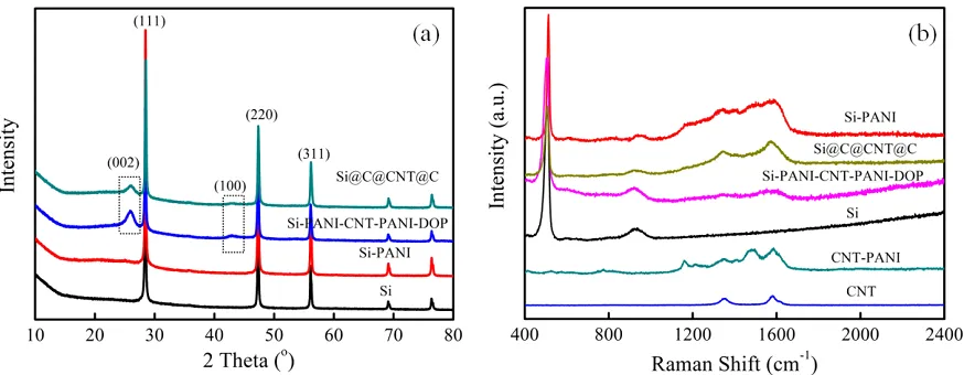
Fig. 1(a) is the X-ray diffraction (XRD) patterns of Si, Si-PANI, Si-PANI-CNT-PANI-DOP and Si@C@CNT@C. The major diffraction peaks at 28.5o ,47.5o and 56.3o are in accordance with the index of crystal face of (111), (220) and (311) in crystalline Si, which means that our commercially available SiNPs are well-crystallized and the crystal structure in SiNPs are held during the subsequent polymer coating process and carbonization process. Also, there are two other diffraction peaks around 26o and 42.4o in Si-PANI-CNT-PANI-DOP and Si@C@CNT@C, which can be attributed to the index of crystal face of (001) and (100) of CNTs [40].
Figure 1. (a) XRD patterns of Si nanoparticles, Si-PANI, Si-PANI-CNT-PANI-DOP and Si@C@CNT@C; (b) Raman spectra of Si nanoparticles, Si-PANI, CNT, CNT-PANI, Si-PANI-CNT-PANI-DOP and Si@C@CNT@C.
[image:4.596.93.505.99.238.2] [image:4.596.80.517.404.574.2]
about 1591 cm-1 and 1351 cm-1 reappear in Si@C@CNT@C derived from the carbonization of Si-PANI-CNT-PANI-DOP. Two peaks at about 1591 cm-1 and 1351 cm-1 of carbon materials in Raman spectra
[image:5.596.194.401.188.683.2]are the results of the bond stretching of sp2 bound carbon atoms in both rings and chains or the breathing modes of sp2 bound carbon atoms in hexa-carbon ring in graphite plane [42]. Therefore, these two Raman peaks only appears in Si@C@CNT@C meaning that Si-PANI-CNT-PANI-DOP has totally transformed into Si@C@CNT@C after the microwave-assisted pyrolysis treatment.
Nanoparticles tend to aggregate and Fig. 2(a) exhibits the image of bare SiNPs that gather together forming small aggregates. Also, the size distribution of bare SiNPs varies from around 50 nm to 200 nm. Fig. 2(b) shows a bigger volume of Si-PANI than primary bare SiNPs. The morphologies of CNT and CNT-PANI are shown in Fig. 2(c) and Fig. 2(d). The obvious difference between CNT and CNT-PANI is seen that CNT-PANI holds larger surface roughness. The morphology of Si-PANI-CNT-PANI-DOP is shown in Fig. 2(e) and the carbonized product of Si-PANI-CNT-Si-PANI-CNT-PANI-DOP, Si@C@CNT@C, is also listed in Fig. 2(f). It can be clearly seen that Si is well dispersed and bounded onto CNT. In addition, TEM was used to analyse the joint structure between Si and CNT in Si@C@CNT@C. As shown in Fig. 2(g-h), Si is attached to CNT like the tree buds on the branches. The magnified TEM picture of Si@C@CNT@C in Fig. 2(i) directly demonstrates that both Si and CNT are covered by a uniform carbon coating and Si is firmly anchored onto the surface of CNT by the merged surface carbon coating. The joint structure of Si and CNT in Si@C@CNT@C shown in Fig. 2(i) would give well electron transport pathways and the carbon coating layer will also prevent the electrolyte from reacting with Si directly during the electrochemical cycling.
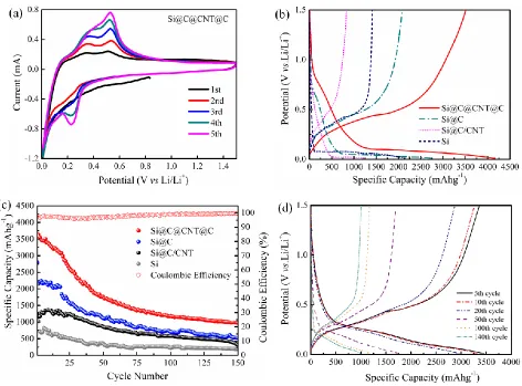
The electrochemical property of Si@C@CNT@C was shown in Fig. 3(a) and it was different from that of Si electrode that we reported before [43]. In the cathodic part of first cycle, a weak peak at 0.65 V is ascribed to the formation of SEI resulted in the initial irreversible capacity [44, 45]. In the subsequent cycles, only one cathodic peak at 0.22 V is observed and keeping enhanced due to the amorphization process of crystalline Si during the initial lithiation process and the lithium ion insertion into the amorphous silicon [46]. The anodic part displays two peaks at 0.34 V and 0.52 V, corresponding to the dealloying reaction of Li-Si alloy and the formation of amorphous Si, respectively [47, 48]. While Si electrode only shows very weak and broad anodic peak which indicates that the lithium ion de-insertion from silicon anode is a sluggish process [43].
Fig. 3(b) shows the first discharge/charge voltage profiles of Si, Si@C, Si@C/CNT (mixture of Si@C and CNT) and Si@C@CNT@C electrodes within voltage domain of 0.01~1.5 V (vs. Li/Li+) and a current density of 0.42 Ag-1. Si, Si@C, Si@C/CNT and Si@C@CNT@C electrodes show a first discharge capacity of 2143 mAhg-1, 2801 mAhg-1, 1254 mAhg-1 and 4162 mAhg-1, respectively. Then the correlated first cycle coulombic efficiency (CE) of Si, Si@C, Si@C/CNT and Si@C@CNT@C electrodes is calculated by the formula “charge capacity/discharge capacity*100%”, demonstrating the CE value of 66%, 74%, 64% and 84%, respectively. The value of CE can be used to estimate the effective utilization efficiency of active material in the charge/discharge cycle. Therefore, the improved CE of Si@C@CNT@C electrode indicates that the structure of carbon coating layer anchoring Si onto CNT can effectively enhance the utilization efficiency of active material in the charge/discharge cycle.
Under the test condition of current density of 0.42 Ag-1 between 0.01 V and 1.5 V(Fig. 3(c))
capacity around 1000 mAhg-1 after 150 cycles. The improved cycle performance of Si@C@CNT@C electrode is attributed to the anchored structure between Si and CNT.
Some available results of SiNPs/CNT composite reported in the literature are summarized in table 1 for comparison with this work, and Si@C@CNT@C electrode still shows a fine performance. From the corresponding CE curve of Si@C@CNT@C electrode shown in Fig. 3(c), the value of CE rapidly increases from 84% to 95% for the second cycle, and then reaches near 100%. Fig. 3(d) exhibits the discharge/charge voltage curves of Si@C@CNT@C electrode from the 5th to the 140th cycle. The discharge potential plateau shown in Fig. 3(b) disappears and is replaced by a group of slope curves due to the Si structure changes from crystal to amorphous process during the first discharge process.
[image:7.596.67.539.257.606.2]
Table 1. Performance of Si@C@CNT@C comparing with other types of Si-CNT anode
Active materials
Initial discharge
capacity (mAhg-1)
Rate performance Cycle performance
ref Capacity(mAhg-1) /
discharge current (Ag-1)
Capacity(mAhg-1) /100
Cycles
Si/MWCNT 3480 n/a 620 49
Si/GR/MWCNT 2609 n/a 425 50
CNT-Si 2200 900/3.6 1100 51
Si/MWCNTs 2014 900/2 938 52
Si-MWCNT@C 1936 1008/2 1164 53
Si@C@CNT@C 4162 1750/4.2 1240 This work
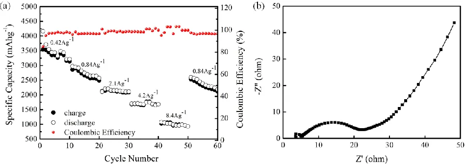
Fig. 4(a) reveals the rate capability of Si@C@CNT@C electrode at different discharge/charge current densities ranging from 0.42 Ag-1 to 8.4 Ag-1. The electrode demonstrates a high discharge capacity of 3000 mAhg-1, 2500 mAhg-1, 2100 mAhg-1, 1700 mAhg-1 and 1000 mAhg-1 under the corresponding discharge current densities of 0.42 Ag-1, 0.84 Ag-1, 2.1 Ag-1, 4.2 Ag-1and 8.4 Ag-1, respectively. After the high rate discharge/charge cycling at 8.4 Ag-1 for 10 cycles, the specific capacity can get back to around 2200 mAhg-1 when the discharge current decreases to 0.84 Ag-1. The CNTs networks provide fast channel for electron transfer and therefore enabled high power rate capacity. Additionally, the corresponding CE maintains nearly 100% even at high discharge/charge current density of 8.4 Ag-1. The electrochemical impedance spectrum (EIS) of Si@C@CNT@C electrode (shown in Fig. 4(b)) also act as a supplementary that Si@C@CNT@C electrode presents a small surface layer resistance, which would benefit from the improved electron transfer in the anchored structure between Si and CNT linked by carbon coating layer in the whole electrode.
[image:8.596.63.537.549.716.2]
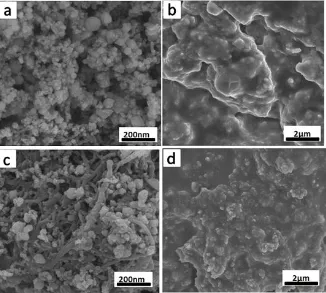
Figure 5. SEM images of prepared electrode. (a) fresh Si electrode; (b) Si electrode after 60 cycles; (c) fresh Si@C@CNT@C electrode; (d) Si@C@CNT@C electrode after 60 circles.
Fig. 5 (a) and (c) present the SEM images of fresh electrode prepared by Si and Si@C@CNT@C, respectively. The electrode slurry was manually scraped onto the Cu foil and without additional roller-compression process, so all the fresh electrodes demonstrate a porous morphology. And the fresh Si@C@CNT@C based electrode clearly shows that SiNPs clusters are anchored on the CNTs. After 60 cycles of charge/discharge process, both the electrodes exhibit a similar surface morphology. But large-size silicon is observed in the Si based electrode (Fig. 5(b)). Si nanoparticles were easily experienced an electrochemical sintering process and resulted in irreversible capacity loss [20, 21]. The SiNPs merge together with the neighbouring SiNPs and aggregate into large-size silicon during the whole lithium insertion and extraction process. While the anchor structure that Si@C attached onto CNT in Si@C@CNT@C not only acts as an important role for enhancing the conductivities performance of SiNPs, it also can provide a buffer layer and prevent the aggregation behaviour of SiNPs during the whole charge/discharge cycle.
4. CONCLUSIONS
Hence, Si@C@CNT@C composite showed a high initial discharge specific capacity of ~4162 mAhg-1 and initial coulombic efficiency of 84%. Because of the anchor effect between CNT/carbon layer and SiNPs, Si@C@CNT@C present excellent rate performance and even high discharge capacity of 1000 mAhg-1 under the corresponding discharge current density of 8.4 Ag-1. In the cycle performance test, Si@C@CNT@C based electrode demonstrates reversible lithium storage of ~1000 mAhg-1 after 150 cycles. In addition, the cycle performance may be further enhanced by setting a proper void set between the silicon and carbon shell in Si@C@CNT@C.
ACKNOWLEDGEMENTS
This work was supported by the China Postdoctoral Science Foundation (2015M572354), Shenzhen Advanced Technology Ceramic Engineering Lab (Director) Open Fund (T201506), National Natural Science Foundation of China (Nos. 51202150, 21703141 and 51272161), Program of Introducing Innovative Research Team in Dongguan (No.2014607109), foundation of the State Key Laboratory of Solidification Processing in NWPU (SKLSP201110) and Shenzhen Basic Research Program (No. JCYJ20170818101932570, JCYJ20170818100134570,JCYJ20170817102025753).
References
1. W. Li, X. Sun, Y. Yu, Small Methods, 1 (2017) 1600037
2. Y. An, H. Fei, G. Zeng, L. Ci, S. Xiong, J. Feng, ACS Nano, 12 (2018) 4993-5002
3. J. Liu, N. Li, M. D. Goodman, H. G. Zhang, E. Epstein, B. Huang, Z. Pan, J. Kim, J. H. Choi, X. Huang, J. Liu, K. J. Hsia, S. J. Dillon, P. V. Braun, ACS Nano, 9 (2015) 1985-1994
4. K. Ababtain, G. Babu, S. Susarla, H. Gullapalli, N. Masurkar, P. M. Ajayan, L. M. R. Arava, Mater. Res. Express, 5 (2018) 014004
5. J. K. Lee, C. Oh, N. Kim, J. Hwang, J. Mater. Chem. A, 4 ( 2016) 5366–5384
6. J. Li, Q. Xu, G. Li, Y. Yin, L. Wan, Y. Guo, Mater. Chem. Front., 1 (2017) 1691-1708
7. X. Li, M. Gu. S. Hu, R. Kennard, P. Yan, X. Chen, C. Wang, M. J. Sailor, J. Zhang, J. Liu, Nat. Commun., 5 (2014) 1-7
8. B. Kim, J. Ahn, Y. Oh, J. Tan, D. Lee, J. Lee, J. Moon, J. Mater. Chem. A, 6 (2018)3028-3037 9. O. Rahaman, B. Mortazavi, T. Rabczuk, J. Power. Sources, 307 (2016) 657-664
10. C. Shen, X. Fang, M. Ge, A. Zhang, Y. Liu, Y. Ma, M. Mecklenburg, X. Nie, C. Zhou, ACS Nano, 12 (2018) 6280-6291
11.R. Kumar, P. Lu, X. Xiao, Z. Huang, B. W. Sheldon, ACS Appl. Mater. Interfaces, 9 (2017) 28406−28417
12.S. P. Nadimpalli, V. A. Sethuraman, G. Bucci, V. Srinivasan, A. F. Bower, P. R. Guduru, J. Electrochem. Soc., 160 (2013) A1885-A1893.
13.M. Wetjen, D. Pritzl, R. Jung, S. Solchenbach, R. Ghadimi, H. A. Gasteiger, J. Electrochem. Soc., 164 (2017) A2840-A2852.
14.T. Yoon, C. C. Nguyen, D. M. Seo, B. L. Lucht, J. Electrochem. Soc., 162 (2015) A2325-A2330. 15.Y. Xu, E. Swaans, S. Chen, S. Basak, P. P. R. Harks, B. Peng, H. W. Zandbergen, D. M. Borsa, F. M.
Mulder, Nano Energy, 38 (2017) 477-485
16.L. Cui, Y. Yang, C. Hsu, Y. Cui, Nano Lett., 9 (2009) 3370-3374 17.M. Ko, S. Chae, J. Cho, ChemElectroChem, 2 (2015) 1645-1651
18.X. H. Liu, L, Zhong, S. Huang, S. X. Mao, T. Zhu, J. Y. Huang, ACS Nano, 6 (2012) 1522-1531 19.L. Hu, N. Liu , M. Eskilsson, G. Zheng, J. McDonough, L. Wågberg, Y. Cui, Nano Energy, 2 (2013)
138-145.
ACS Nano, 6 (2012) 8439–8447
21.L. Luo, J. Wu, J. Luo, J. Huang, V. P. Dravid, Sci. Rep., 4 (2014) 3863
22.J. Xie, L.Tong, L.Su, Y. Xu, L. Wang, Y. Wang, J. Power. Sources, 342 (2017) 529-536
23.T. Yang, X. Tian, X. Li, K. Wang, Z. Liu, Q. Guo, Y. Song, Chem. Eur. J., 23 (2017) 2165-2170 24.U. Toçoğlu, G. Hatipoğlu, M. Alaf, F. Kayış, H. Akbulut, Appl. Surf. Sci., 389 (2016) 507-513. 25.G. H. An, H. Kim, H. J. Ahn, ACS Appl. Mater. Interfaces, 10 (2018) 6235-6244
26.Y. Wu, J. Wang, K. Jiang, S. Fan, Front. Phys., 9 (2014) 351-369. 27.P. Sehrawat, C. Julien, S. S. Islam, Mater. Sci. Eng. B, 213 (2016) 12–40
28.L. Xue, G. Xu, Y. Li, S. Li, K. Fu, Q. Shi, X. Zhang, ACS Appl. Mater. Interfaces, 5 (2012) 21–25 29.N. T. Hieu, J. Suk, D.W. Kim, J. S. Park, Y. Kang, J. Mater. Chem. A, 2 (2014) 15094–15101 30.K. Fu, O. Yildiz, H. Bhanushali, Y. Wang, , K. Stano, L. Xue, X. Zhang, P. D. Bradford, Adv. Mater.,
25 (2013) 5109-5114.
31.L. F. Cui, L. Hu, J. W. Choi, Y. Cui, ACS Nano, 4 (2010) 3671-3678. 32.W. Wang, P. N. Kumta, ACS Nano, 4 (2010) 2233–2241
33.G. Grinbom, M. Muallem, A. Itzhak, D. Zitoun, G. D. Nessim, J. Phys. Chem. C, 121 (2017) 25632-25640.
34.Y. Wen, Y. Zhu, A. Langrock, A. Manivannan, S. H. Ehrman, C. Wang, Small, 9 (2013) 2810-2816. 35.L. Xiao, Y. H. Sehlleier, S. Dobrowolny, H. Orthner, F. Mahlendorf, A. Heinzel, C. Schulz, H.
Wiggers, ChemElectroChem, 2 (2015) 1983-1990
36.W. S. Kim , J. Choi, S. H. Hong, Nano Res., 9 (2016) 2174-2181.
37.N. Gospodinova, L. Terlemezyan, Prog. Polym. Sci., 23 (1998) 1443-1484
38.H. Wu, G. Yu, L. Pan, N. Liu, M. T. McDowell, Z. Bao, Y. Cui, Nat. Commun., 4 (2013) 1-6 39.X. Yu, H. Fan, Y. Liu, Z. Shi, Z. Jin, Langmuir, 30 (2014) 5497-5505
40.A. Cao, C. Xu, J. Liang, D. Wu, B. Wei, Chem. Phys. Lett., 344 (2001) 13-17
41.S. Zeng, H. Chen, F. Cai, Y. Kang, M. Chen, Q. Li, J. Mater. Chem. A, 3 (2015) 23864-23870 42.A. C. Ferrari, J. Robertson, PRB., 61 (2000) 14095-14107
43.G. Fang, X. Deng, J. Zou, X. Zeng, Electrochimica Acta, 295 (2019) 498-506
44.J. Xie, L. Tong, L. Su, Y. Xu, L. Wang, Y. Wang, J. Power. Sources, 342 (2017) 529-536 45.J. J. Wu, W. R. Bennett, NASA/TM-2012-217739,
46.K. W. Schroder, H. Celio, L. J. Webb, K. J. Stevenson, J. Phys. Chem., C 116 (2012) 19737−19747 47.L. Y. Yang, H. Z. Li, J. Liu, Z. Q. Sun, S. S. Tang, M. Lei, Sci. Rep., 5 (2015) 10908
48.J. Li, J. R. Dahn, J. Electrochem. Soc., 154 (2007) A156-A161
49. U. Tocoglu, O. Cevher, H. Akbulut, Acta. Phys. Pol. A, 127 (2015) 1059-1061
50. U. Tocoglu, G. Hatipoglu, M. Alaf, F. Kayls, H. Akbulut, Appl. Surf. Sci., 389 (2016) 507-513 51. D. N. Ho, O. Yildiz, P. Bradford, Y. Zhu, P. S. Fedkiw, J. Appl. Electrochem., 48 (2017) 127-133 52. Y. Jiang, H. Wang, B. Li, Y. Zhang, C. Xie, J. Zhang, G. Chen, C. Niu, Carbon, 107 (2016) 600- 606