Rochester Institute of Technology
RIT Scholar Works
Theses Thesis/Dissertation Collections
8-1-2009
Course grained low power design flow using UPF
Archana VaranasiFollow this and additional works at:http://scholarworks.rit.edu/theses
This Thesis is brought to you for free and open access by the Thesis/Dissertation Collections at RIT Scholar Works. It has been accepted for inclusion in Theses by an authorized administrator of RIT Scholar Works. For more information, please [email protected].
Recommended Citation
Course grained Low Power Design Flow Using UPF
by
Archana Varanasi
A Thesis Submitted in Partial Fulfillment of the Requirements for the Degree of Master of Science in Computer Engineering
Supervised by
Dr. Dhireesha Kudithipudi Department of Computer Engineering
Kate Gleason College of Engineering Rochester Institute of Technology
Rochester, NY August 2009
Approved By:
_____________________________________________ ___________ ___
Dr. Dhireesha Kudithipudi
Primary Advisor – R.I.T. Dept. of Computer Engineering
_ __ ___________________________________ _________ _____
Dr. Kenneth Hsu
Secondary Advisor – R.I.T. Dept. of Computer Engineering
_____________________________________________ ______________
Dr. Pratapa Reddy
Thesis Release Permission Form
Rochester Institute of Technology
Kate Gleason College of Engineering
Title: Course grained Low Power design flow using UPF
I, Archana Varanasi, hereby grant permission to the Wallace Memorial Library to
reproduce my thesis in whole or part.
_________________________________ Archana Varanasi
Acknowledgements
I would like to thank my advisor, Dr. Dhireesha Kudithipudi for her continued and
Abstract
Increased system complexity has led to the substitution of the traditional bottom-up design flow by systematic hierarchical design flow. The main motivation behind the evolution of such an approach is the increasing difficulty in hardware realization of complex systems.
With decreasing channel lengths, few key problems such as timing closure, design sign-off, routing complexity, signal integrity, and power dissipation arise in the design flows. Specifically, minimizing power dissipation is critical in several high-end processors. In high-end processors, the design complexity contributes to the overall dynamic power while the decreasing transistor size results in static power dissipation.
This research aims at optimizing the design flow for power and timing using the unified power format (UPF). UPF provides a strategic format to specify power-aware design information at every stage in the flow. The low power reduction techniques enforced in this research are multi-voltage, multi-threshold voltage (Vth), and power gating with state retention. An inherent design challenge addressed in this research is the choice of power optimization techniques as the flow advances from synthesis to physical design. A top-down digital design flow for a 32 bit MIPS RISC processor has been implemented with and without UPF synthesis flow for 65nm technology. The UPF synthesis is implemented with two voltages, 1.08V and 0.864V (Multi-VDD). Area, power and timing metrics are analyzed for the flows developed.
Table of Contents
Chapter 1 Digital design flows………1
Introduction……….1
Summary……….7
Chapter 2 Background and Motivation………9
Challenges in existing design flows……….10
Existing design flows………...11
Low power techniques……….17
Unified power format (UPF)………...20
Motivation………....22
Thesis goals………..23
Summary………..24
Chapter 3 Aspects of a design flow………....25
Synthesis………25
Physical design………..29
Chapter 4 Test Platform………43
Top-down standard digital design flow……….45
UPF synthesis……….……48
Chapter 5 Results and analysis………..………52
Top-down standard digital design flow…………....52
UPF synthesis………...…….59
Chapter 6 Conclusions and future work……….63
Conclusions………63
List of Figures
Figure 1.1: Process size versus delay……….3
Figure 1.2(a): Conventional design flow..………….….4
Figure 1.2(b): Present design flow…..………..………..4
Figure 2.1: Synthesis centric flow...………...11
Figure 2.2: Physical design centric flow.………...12
Figure 2.3: Unification based flow………....13
Figure 2.4: Power reduction technique-Clock gating...17
Figure 2.5: Power reduction technique-Power gating..17
Figure 2.6: Unified power format...……….19
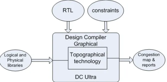
Figure 3.2: RTL synthesis tool – Design compiler…....27
Figure 3.3: Clock tree synthesis……….………...34
Figure 3.4: Physical design tool – IC compiler.……....36
Figure 3.5: Extraction tool………....37
Figure 3.6: Static timing analysis tool………..38
Figure 3.7: UPF special cells……...……….40
Figure 4.1: 32-bit MIPS RISC processor.………44
Figure 4.2: Implementation directory structure……...45
Figure 4.3: Power intent specification (UPF)………..49
Figure 5.1: Area in top-down design flow…...……...54
Figure 5.2: Voltage drop map………...55
Figure 5.3: Power in top-down design flow ...…56
Figure 5.5: Fully routed 32-bit RISC processor..…...58
Figure 5.6: Area in UPF synthesis flow………. 60
Figure 5.7: Power in UPF synthesis flow ...….62
List of Tables
Table 5.1: Results for top-down design flow.………….53
Table 5.2 UPF synthesis Vs top-down design flow…....59
Glossary
Chapter 1
Digital Design Flows
This chapter discusses the evolution of design flows and the effects of design
complexity on the design flows. The effect of various design metrics for shrinking
process technologies and a fundamental digital design flow are explained in section 1.1.
The summary of this chapter and the rest of the thesis document structure are presented in
section 1.2.
1.1. Introduction
A physical design flow consists of synthesizing a register transfer level (RTL)
functional description of a design and the process of physical implementation on the
design to obtain a production-worthy functionally correct layout. This output layout file
is then sent out to the fabrication process. In the traditional methods of converting a
transistor-level functional description of a design to a layout level of abstraction, there
were no concrete design flows that existed [6]. All the circuit schematics were drawn by
hand, and were laid out with their respective metal descriptions- to obtain a complete
layout. This included the process of laying out transistors, resistors, capacitors, and even
the interconnect between them [6]. Interconnect refers to the point-to-point connection
between different cells or components in the design.
As the design functionality increased with time, the increasing number of
transistors and the various challenges encountered at such small device lengths led to the
formulation of a strategic design flows to implement synthesis and physical design for a
With a complete layout for a design in place, it is very important to consider the
effects of shrinking process technologies. Some of the important challenges at reduced
channel lengths are crosstalk noise effect, delay effects and leakage power.
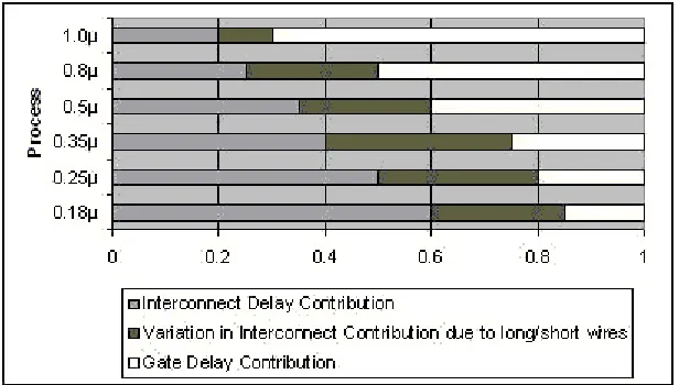
The most significant metric that is to be taken care due to interconnect at process
technologies under 180nm is the Crosstalk noise effect. Interconnect in the design leads
to laying out long metal wires through the design. Crosstalk noise is the result of placing
the metal wires in interconnects close to each other in the physical design process. As the
channel lengths scale down, so do the interconnect properties which contribute
significantly to the gate delays in the design with the principle that, longer the metal wire,
more is the delay in that segment. The delay contribution as the channel lengths reduce is
shown in Figure 1.1 [26]. This delay effect hence affects the timing of the design – also a
critical design metric.
Apart from the delay-interconnect problems, another important design metric
affect to be considered is power. As the device length decreases, the leakage power
contribution to the total power dissipation in the design increases. Techniques to achieve
low power solutions are incorporated in design flows.
Above mentioned are some of the challenges associated with technology
scale-down. Design flow challenges are described in detail in Chapter 2.
Specifically, as the designs scaled from Small Scale Integration (SSI)
technologies to Very Large Scale Integration (VLSI) technologies, the need for design
Figure 1.1 Process Size versus Delay
A design flow was hence devised to reduce the effects of these challenges in the
traditional methods. Design flows consisted of mainly two steps, logic synthesis and
physical design. With the evolution of smarter synthesis and physical design tools, efforts
are made to integrate these processes into one complete design flow to obtain a
production worthy layout for all the challenges encountered at every stage. It has become
of much importance that there exists a strong correlation between the logic synthesis and
physical design, the reason being that the synthesis does not account for the physical
design aspects and performs only logic optimization on the design.
Initially, the design flows were broken up into two phases, front-end dealt by the
designer and the back-end was taken care of by the application specific integrated circuits
(ASIC) vendors. While the designers held the complete responsibility of the logical
aspect of the design, the implementation process was handed over to the ASIC vendors.
take over the responsibility for the physical design phase along with the front-end design,
enabling them to have a better understanding of the end layout functionality and metrics
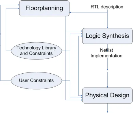
associated with it. Figure 1.2(a) and Figure 1.2(b) [19] depicts the conventional design
flow and Floorplan driven design flow respectively [36], which is what is followed in
most design flows today.
[image:16.612.215.431.227.421.2] [image:16.612.220.445.476.667.2]As seen in the Figure 1.2(a), the conventional design flow had no knowledge
sharing concept between logic synthesis and physical design. The synthesized netlist is
carried forward to the layout processes not accounting for any tight correlation of design
metrics between the two processes. Whereas, the present design flows have a feedback
loop between the logic optimization and implementation, which enables the synthesis tool
to better analyze the design based on its placement and routing properties for
optimization at the logic level. This refers to the floorplanning of the design in the
physical design stage. Based on the synthesized netlist, the die area, core area and pin
constraints are set which are fed back to the synthesis tool to obtain a better optimized
netlist. This leads to multiple iterations between them to achieve the required timing
closure and expected power dissipation but in turn increases the time-to-market.
An overview of the basic flow, used in this research is discussed in Chapter 3.
The register transfer level verilog/VHDL functional description for a design based on its
specifications is written and synthesized [5] . Other inputs to the synthesis tool include
design constraints specified by the user and the technology library files. The optimized
gate level netlist that is a result of the synthesis then goes through the physical design
process to obtain the final layout of the desired product. The same set of constraints and
library setup that is used for the synthesis of the design is used in the physical design
1.2. Summary
In this chapter, the importance and significance of a digital design flow setup is
presented. The rest of the thesis draft is organized as follows. Chapter 2 will discuss the
background and existing design flows and the motivation in developing the design flows
and substantiate its efficiency. Chapter 3 will describe the implementation methodology
details, the various stages involved in a digital design flow and the tools related to it
along with an introduction to the UPF synthesis. Chapter 4 will discuss the test platform
to implement these flows- 32-bit MIPS RISC processor. Chapter 5 will present the
simulation results and analysis. Finally, chapter 6 will provide conclusions on the
Chapter 2
Background and Motivation
2.1. Challenges in existing design flows
One of the major concerns in design flows is to maintain the completeness of the
flow by correlating the logic synthesis and physical design. With the shrinking process
technologies, integrating the design synthesis and the physical implementation into a
complete design flow and performing power analysis of the design post physical design is
becoming a more and more cumbersome task [2][34]. Some of the persisting challenges
that led to the formulation of the existing flows are timing closure, area, signal integrity
or crosstalk effects, leakage power and design complexity.
As the process-size reduces, the room for more interconnect and gates to
implement the design is restricted which leads to having a tight user constraints on the
design [13]. As a result of this, at process technologies beyond 65nm, it is very important
to achieve a good timing closure on the design. Although the synthesis follows a standard
wire load model technique to estimate the physical design delays, there always exists a
mismatch of gate delays after the physical implementation stage.
One of the main reasons that motivate designers to go down in device lengths in
the deep sub-micron (DSM) processes along with speed is the overall design area metric.
The die area is specified in the design planning stage of the implementation process based
on the estimate out of synthesis. For a given die area, when the metal layers are placed
very close to each other, the interlayer coupling capacitance effects also have to be
known to have been four times larger than the inter-layer capacitance in the year 2002
and is predicted to rise to about 6 times or more in 2010 [7].
Same layer coupling capacitances are nothing but crosstalk effects resulting
because of the close proximity in the interconnect wiring. With reducing technology, the
space between metal layer routing also reduced hence leading to this. This also
contributes to the electro migration, antenna effects and IR drop in the design.
All the above mentioned effects in turn contribute to the total power in the design.
For the same design, at different process technologies, the leakage power is an important
challenge to deal with. Depending on the design, the leakage power alone may contribute
up to 10% of the total power at a lower process technology which is highly undesirable
because that will lead to a lot of heat dissipation in the silicon.
Hence, design flows are constantly being susceptible to changes based on these
design challenges. When the complexity of the design increases, there is a scalability
problem. As the design becomes more complex, the resources that take up to synthesize
and layout the design in the most efficient way is a problem considering the limitations.
Even with the most optimistic solution results out of synthesis, there is always a struggle
to close the correlation loop with the physical design stage in a design flow. With more
sub-modules in the design, it calls for a hierarchical design flow where every metric for
each of the individual sub-modules should be considered for an overall clean top-level
design. Examples of such designs are high performance processors which include
2.2. Existing design flows
Design Implementation has been through a lot of changes since when it started as
proposing drafting techniques that specified every basic component and their
interconnections. The main reason behind this is the increasing complexity of the circuit
designs and physical realization of the same with the existing techniques. Hence, the
traditional methods were soon; and are being replaced with the evolving implementation
flows. Increased design complexity includes design constraints, process variables and
other significant features which may be design dependent. At every stage in the flow, it is
important to adapt to newer techniques for better optimization of the design in the
back-end. This leads to the efficient use of design automating tools. As the channel lengths
reduced, circuit designers handling these CAD tools experienced new set of challenges.
To help manage the complexity of synthesizing large designs at such small device
lengths, circuit designers make extensive utilization of these design automation tools. The
implementation flow that comprises of the logic synthesis and the physical design hence
runs through a number of iterations before converging to an optimum solution.
As discussed in Chapter 1, the basic VLSI flow starts with
Register-Transfer-Level logic to laying out the design followed by design verification. Every level has its
own importance to arrive at an optimum solution with respect to the various metrics of
the design such as area, power and timing. This requires a design engineer to provide the
most efficient flow to yield the best results. Hence, flows are being iteratively developed
based on the complexity of the design and convergence between the logic synthesis and
Due to the persisting challenges like timing closure, signal integrity and capacity,
design flows have been evolving ever since to reduce these difficulties at every step.
Some of the current design flows in use are explained in the following sections.
2.2.1 Synthesis centric
The synthesis centric design flow is an approach where the synthesis process
mainly drives the design flow [34]. The synthesis process provides the designer with area
estimates based on floorplan details fed to the synthesis tool as a result of compiling the
design to logic gates. This is still the area of only the placed gates and the physical design
engineer may then chose to pick the die area estimating the routing area depending on the
complexity of the design. A standard wire- load model may also be used as a solution to
estimate delays, but this does not contain the physical information for every logic gate in
the design which will lead to a difference in the metric estimates of the design after the
implementation stage. It is necessary to ensure that the synthesis tool should be capable
of yielding a valid implementation without violating any of the constraints. This approach
performs more iteration with synthesis in the flow at different coarseness levels and
constraints and then proceeds to the physical implementation to be as close to a perfect
Figure 2.1 Synthesis centric flow
2.2.2 Physical design centric
In this kind of design flow, the implementation process drives the flow [34]. A
synthesized netlist is partitioned into blocks for placement- an optimization technique
while floorplanning is done. After placement, several delay estimates from global routing
and congestion reports prior to routing can be extracted from the design. These delays
may be fed back to the synthesis process as wire load models or floorplan constraints for
the synthesis tool to compile and give out a much correlated output netlist for the
physical design process. This way, it can be ensured that the logic optimization phase is
in a close loop configuration with the physical design process. This repetitive synthesis
can be done at different stages in the implementation phase namely after floorplanning,
after placement, and after routing. Figure 2.2 [34] depicts the physical design driven
Figure 2.2 Physical design centric flow
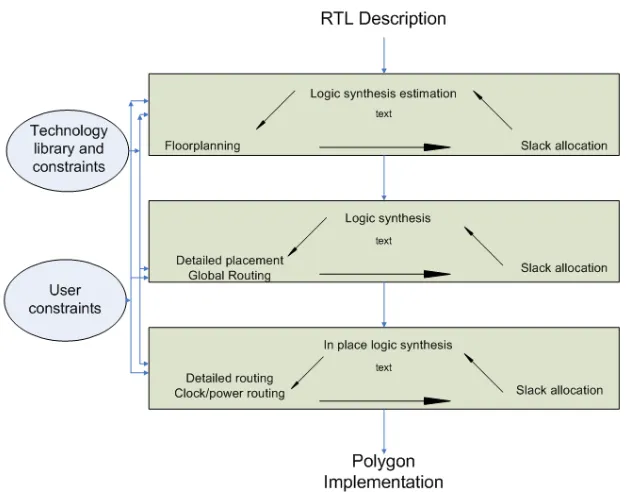
2.2.3 Unification based
The unification based design flow may be treated as design flow that is driven by
both the logic optimization synthesis and the physical design phase [34]. Continuous
iterations are performed between the two phases until a highly correlated and optimized
design solution is achieved. This implies that after a certain number of iterations, the
design metrics reported after synthesis are as good as the ones reported after the
placement and routing process of the design. The unification based design flow is shown
Figure 2.3 Unification based design Flow
2.2.4 Custom wire load model
The above three design flows being the basic models of the existing design flows,
this kind of design flow and the ones further explained may also be considered as a part
of them. This design flow allows the designer to input a delay wire load model for the
design so that the synthesis process has a better estimate of the delays when compiling
the design and hence does a better job in providing an optimized netlist [7]. After a single
iteration of the place-and-route process is done, the synthesis is now fed with the real
wire load models in the next iteration. This tends to change the design metrics of the
design to achieve more accuracy.
2.2.5 Block-assembly flow
timing individually and then optimized at the top-level assuming that the delay between
the sub-modules is not that significant. This approach uses a statistical wire load model,
which is just an assumed estimate of the delays in the design and hence may not be able
to prove it to be a highly correlated design flow. But this is still used for its ability to
perform hierarchical synthesis which gives the designer the block-level metric details to
improve the top-level picture of the design even though it might result in routing
congestion in the implementation phase [7].
2.2.6 Constant delay synthesis flow
In this flow, the logic gate delays are expressed as a function of gain in the
synthesis process, which is the ratio of the output capacitance the gate can drive to its
input pin capacitance. These delays are fixed within the logic gates when performing
synthesis of the design. This synthesized netlist is then placed and routed. This kind of
design flow, still not being an efficient one with fixed gate delay estimations will not
match any of their corresponding delay values in the physical design stage leading to a
congested design. The delays then have to be stretched a little in their allowed margin to
re-do the flow to achieve a better design solution [7].
2.2.7 Placement aware synthesis
As the name suggests, in this flow the constraint requirements on the design
metrics are fed after the placement process to the synthesis tool. This is still not
2.2.8 Refinement-based flow
For a given design, it has become very important to achieve high QoR (quality of
results) considering all the design metrics like power, area and timing. Starting with a
course grained flow where the placement and routing details have the most minimum
information, it develops in to a fine grained flow until the placement and routing details
are final. All the metrics mentioned above are monitored after every stage in between
these two points [7]. Hence, the design converges into a complete design flow.
2.2.9 Layout driven synthesis
With the shrinking process technologies, it has become of prime importance that
the parasitics are also considered when performing synthesis on a design. Along with the
iterative and recursive synthesis-physical design loop, the feedback mechanism is not
restricted only to floorplan based synthesis but extended up to parasitic driven or layout
driven synthesis. The parasitics extracted from a fully routed design are fed back to the
synthesis tool for better correlation [36]. Hence, a constrained based layout driven
approach to logic optimization was developed in this flow.
As all the existing design flows explained are concentrated towards developing a
closed loop design flow, they also incorporate some low power techniques at different
stages in the flow to help reduce the total power dissipation in the design.
2.3. Low power techniques
Power reduction can be classified as static power reduction and dynamic power
Common power reduction techniques are multi-VDD, multi-threshold, and clock
gating. These are mostly gate level implemented power reduction techniques. Multi-VDD
being a very effective power reduction process is not so inherent in the past or the current
design flows since it requires several new things in the physical design stage.
Power reduction techniques are also classified as structural and traditional power
reduction methods based on the developments in the methods as the demand for it
increased. Structural power reduction techniques include implementation using
multi-threshold, multi-oxide devices while the traditional methods include clock gating, power
gating, variable supply, and variable device threshold.
Clock gating is employed to reduce the dynamic power dissipation, while
multi-threshold devices are used in the design to reduce the leakage power. Clock gating is a
technique where the sub modules in a design are not clocked when not in use saving a lot
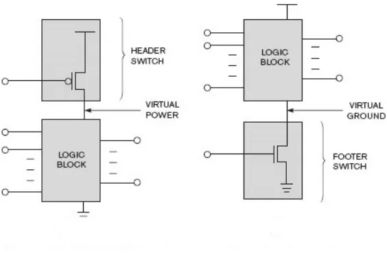
of switching activity in turn reducing the power dissipation. Power gating is a technique
employed when the sub-modules of a design need to be put in a sleep mode when the
functionality of that module is not required. The module has a sleep transistor or the
header transistor (PMOS) from the supply to the module and a footer NMOS transistor.
There are certain requirements for these transistors in size and voltage threshold because
the supply VDD has to pass through this transistor to reach the sub-module. For example,
the sleep transistors should be large enough to support such high current flow through it
when the module supported by it is either switching ON or OFF. More of these
Figure 2.4 Power Reduction Technique – Clock Gating
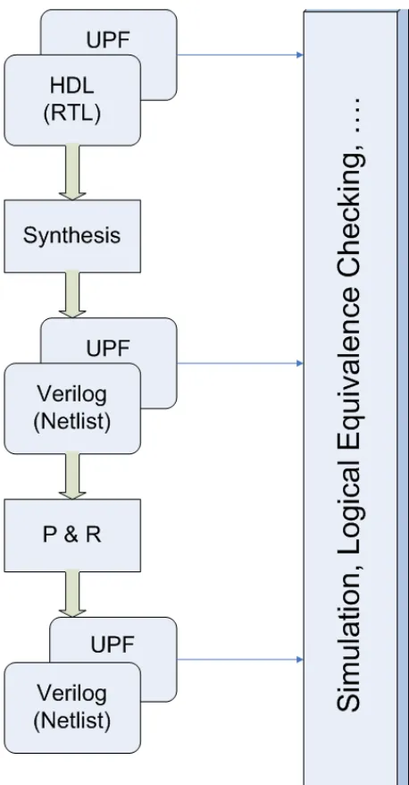
[image:29.612.195.477.380.566.2]2.4. Unified power format
UPF or the Unified power format is an industry wide power format specification
to implement low power techniques in a design flow. Power, becoming an important
factor in today's electronic systems, lead to a need to have a more systematic approach to
reduce power in complex designs.
The UPF deals with setting power domains in a design to achieve power
optimization. It defines both language format and simulation semantics for Power gating.
UPF allows the user to set power domains in a design to achieve power optimization.
Power domains in a design are logic groupings of one or more hierarchical blocks, which
share a power nets hookup requirement, power down control logic, acknowledge signals,
and power switching style. Special scripts are available in the UPF Standard that is used
to create power domains in a design. The power domains are isolated to maintain
predictable output levels using Isolation Cells. It is easier to specify such cells at the
physical design level. Creating power domains in a design at the RTL level is usually a
cumbersome task, but at the synthesis level and the physical design level, the tool makes
it a very feasible task in terms of power optimization. The UPF Standard uses `tcl'
commands that are compatible with the Synopsys synthesis and physical design tools.
The UPF is compatible with these tools at every stage in the flow as shown in Figure 2.6
2.5. Motivation
With the availability of the different kinds of design flows and the increasing
design challenges, a definite flow to integrate the RTL synthesis to the physical design
(placement and routing) to decrease all the challenges faced is an important requirement.
The key design challenges where flows fail to converge are timing and power. Timing is
an issue in the flow at every stage. Even if the placement information is fed to the
synthesis after an initial run, the design will still face routing issues because the
interconnect delays predicted may be inaccurate, or may not be predicted. This drives the
need for a design flow where in it will converge for timing at every stage in the flow with
proper integration of the logic synthesis and physical design.
Power also being an important metric for a design, a power efficient flow along
with timing convergence is required. Static and dynamic power are taken into
consideration as the total power and all possible power reduction techniques are
implemented at a lower level of abstraction along with the implementation of the unified
power format at the chip level. Common power reduction techniques as discussed in the
previous sections are multi-VDD, multi-threshold, and clock gating. They are mostly
implemented at the cell level while the UPF is a power reduction technique that is mostly
2.6. Thesis goals
The goal of this research is to develop two highly correlated design flows.
i) Standard flow - a basic flow setup of the tools and design structure to
perform synthesis, placement and routing on the design with the specified
design constraints.
ii) Power efficient flow that implements the possible power reduction
techniques on the design to follow a systematic solution approach of the
Unified Power Format (UPF).
While design complexity contributes to the overall dynamic power, the decreasing
transistor size is significant for the static power dissipation. Some of the most commonly
used power reduction techniques as explained before are clock gating, multi-VDD and
multi-threshold logic. While these power reduction techniques resolve the issues related
to power optimization in a design, the UPF helps approach them systematically.
The design used to setup the flow is a simple 32 bit MIPS RISC processor. The
tools used to develop the main structure of this flow are Design compiler and IC compiler
by Synopsys. Tools of the same vendor are used for rest of the flow such as verification
and power analysis. Due to the availability of limited libraries, power reduction
techniques like clock gating, multi-threshold and multi-VDD are only implemented. To
use multi-threshold logic in the design, special library cells provided by the tool vendor
are required. The different tools used in this complete Synopsys flow are as shown in
2.7. Summary
This chapter includes some background work on the existing design flows and
challenges faced by them with shrinking process technologies. It introduces the concept
of being able to use low power techniques at different stages in the design flow and
provides a description of the UPF- a systematic approach to integrating low power
techniques in current design flows. It also explains the need to develop a Low power
Chapter 3
Aspects of a design flow
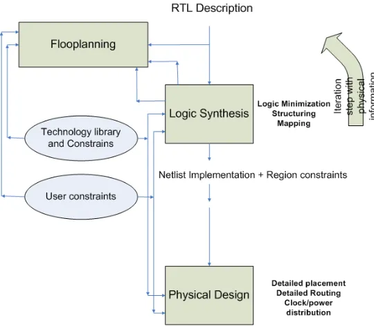
As explained in the background, the main aspects that form a back-end digital
design flow are the logic synthesis and physical design. Figure 3.1 depicts the digital
design flow accounting for the various inputs and outputs at different stages in the flow.
The input and outputs of each stage in the flow and their importance will be discussed in
detail as the flow details progress further. The register-transfer level verilog/ VHDL code
for a desired design or functionality is written and synthesized followed by a detailed
[image:35.612.176.457.329.598.2]placement and routing to obtain the layout for the design.
Apart from the logic synthesis and physical design being important sections of the
flow, it is also of equal importance to perform timing signoff and power signoff on the
designs. Timing signoff check is done to ensure that the critical path in the design is well
within the speed constraints specified at the initial stages of developing the functional
description. Power signoff check is done so that the estimated power dissipation in the
chip is on acceptable levels.
The step following signoff in the flow is design verification. It was evident
enough from the past that, for less complex designs, verification and sign-off did not
really require much of a tool expertise. With the increasing demands on the metrics like
power, area and timing, existing software tools and methodologies are evolving to meet
these challenges at reduced channel lengths.
Each of the verification processes have their own methodologies attached to them
in a flow. There are two forms of verification, property verification and design
verification. Property verification makes sure that the design properties are correct; and
performs design rule checking (DRC) on the design. Design verification ensures the
functionality of the design [31] [3]. The design has to pass through the verification
process before it is sent out to the fabrication process.
This completes the basic description of the digital design flow at all levels of
abstraction. These processes and the tools used to implement the design and the design
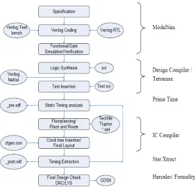
3.1. Synthesis
Synopsys provides more than just logic optimization through its fully developed
synthesis tools. The most commonly used synthesis tool for synthesis is the Design
Compiler. This tool name will be referenced further in the descriptions.
Synthesis is performed on the design by constraining it to some specifications as
required by the design engineer, and a gate level netlist is hence obtained. By mentioning
gate level netlist, it is implied that the obtained verilog/ VHDL file written out by the
synthesis tool will contain logic gates instead of any of the verilog statements that is input
to the tool. Synthesis has also evolved with the increasing design complexity and issues
related with it. The different kinds of synthesis performed are-
3.1.1 RTL synthesis
Synopsys tool Design Compiler operates in different modes to perform different
levels of synthesis. The most common mode of synthesis used by DC (Design Compiler)
is the -xg mode. RTL synthesis and architectural synthesis can be performed using this
mode of operation. RTL synthesis refers to the basic method converting the
verilog/VHDL code to the required digital logic gates to produce a gate level netlist.
Depending on the components in the design, the synthesis tool picks up the necessary
design ware components to implement the design. For example, a design that contains
multipliers and adders when synthesized maps the components to the default multipliers
3.1.2 Architectural synthesis
Architectural synthesis allows the designer to specify the design at an
architectural level, specifying the functionality of high-level building blocks such as
adders, multipliers, and filters[12][20]. This type of synthesis is done when the modules
in a design have to be broken down or partitioned to achieve a better optimized output
design. By partitioning the design in sub-blocks before synthesis, the delay within that
sub-block tends to have a lower value when compared to that when the complete module
is synthesized as one complete block. The Register-transfer synthesis has data path
modules described which when translated to the physical design can be realized as
partitioned blocks or clusters. There are different styles of clustering namely basic
clustering and multi-stage clustering [7].
3.1.3 Floorplan management synthesis
Floorplan management synthesis is performed by the -topo or topographical mode
of the Design Compiler. This mode of operation of the tool allows the user to input a
floorplan constraints file to the tool so that the tool may synthesize the design taking into
account the floorplan details also for the design. For example, if a design has some
memory components that are defined as macros and the placement of these macros is
known and fixed; depending on the position of the macros, the tool will pick the most
optimum solution of cells for the logic connected to the macros from the library. Figure
Figure 3.2 RTL Synthesis tool – Design Compiler
3.1.4 Multi-cycle optimization synthesis
As the name suggests, this type of synthesis is an iterative approach to obtain
maximum correlation between logic synthesis and physical design. To obtain high quality
of results from behavioral synthesis, it is very important that multi-cycle environment be
setup. This ensures a highly optimized design [7].
The different inputs to the tool are discussed further.
3.1.5 RTL
Register transfer level logic -This input of the tool is the design verilog/VHDL
code to be synthesized.
3.1.6 Logical and physical libraries
This is the set of logic gate cells that are given as inputs to the tool. Depending on
the functionality of the design, the different logic gates are picked up by the tool and
implemented. For example, a multiplier in the design upon being synthesized makes the
in a binary format file is the logical information, while physical library information also
includes the layout for every cell described in the binary file. The physical library
information is required when topographical synthesis is done, otherwise it is optional.
3.1.7 Constraints
Every design needs a set of constraints to be synthesized into gates. For example,
every design is associated with a clock speed which can be set in the constraints file so
that the 'clock' pin the design is set to run at that frequency and any violating paths in the
design is reported by the tool to the user enabling the designer to understand how well the
design is implemented in hardware languages and any changes can be made depending
on the outputs. Setting up the clock frequency is one of the most important constraints in
a design. Other constraints include input delays, output delays and setting up a load at the
output ports. The output loads may be an inverter selected from the same library specified
to the tool.
3.1.8 Netlist and output reports
The DC tool outputs a highly correlated netlist file that includes the description of
the design's functionality in the form of gates from the input library file. The output
reports contain the area estimation and timing reports. The area report enables the
designer to have a brief idea of how much the area of the die can be at the physical design
level also considering some routing area. Depending on the complexity of interconnect in
ensures the design is running at a speed higher than the specified clock (constraint file)
and a negative slack reports that the design is not running at a desired frequency and the
path that fails timing.
3.2. Physical design
Post synthesis, the consequent step to develop the design flow is to physically lay
out the optimized netlist of the design using the physical implementation tools. Since this
research aims at developing a complete Synopsys flow, the Synopsys tool used for
physical implementation is the IC compiler. Most commonly known Synopsys tools that
enable us to place and route a given design are Astro, Jupiter and IC Compiler. The IC
Compiler is a single, convergent, chip-level design tool that enables designers to
implement high-performance, complex and challenging designs. As a widely adopted
solution, IC compiler provides best-in-class Quality of Results (QoR), tight sign-off
correlation and powerful Design for Yield (DFY) capabilities. The tool used to formulate
this Design flow is the IC Compiler version A-2007.12. [7][36].
The following are the steps involved in Physical Implementation of a design.
3.2.1 Milkyway library creation
To start with the physical implementation of the design, it is very important to
create a Milkyway library. The Milkyway library contains the cell view and the frame
view for the design. After every step in the physical design process, cells are saved until
the final cell will have the fully implemented design. The frame view refers to the block
design is created and opened to implement the consequent physical design steps. It is a
null directory initially.
Libraries form a very important part in a physical design flow. These are also one
of the most important inputs to the DC tool for synthesis. However, it is sufficient enough
for Design Compiler that the library contains only the standard cell information but no
layouts or cell views for each of them. This means- to physically realize the design with
the library gates, the IC compiler tool or any digital layout tool requires that all the cells
in the library have frame views and cell views in their own Milkyway library. Frame
views of cells contain top level information, but do not go deep into the metal layer
levels, whereas cell views contain the entire cell description including all metal layers.
Usually the standard cells are restricted to the use of METAL1, so that the higher layers
of metal may be used by the tool for routing and power buses. Target libraries should also
be specified in their binary format to be accepted by the tool.
Besides specifying the target libraries, the tool has to be given a tech-file which
contains all the metal layer information that it can use in the following physical design
steps. By metal layer information, it includes attributes like width of the metal, maximum
routing metal layer, minimum routing metal layer and unit tile width.
Now that the digital layout tool has all the standard cell information, it is very
important that each of them have timing models associated with them. These are tluplus
files provided by the library vendor. There exist different corner tluplus files, for example
3.2.2 Importing the design
The optimized netlist that is an output of the RTL synthesis is then imported to
the Milkyway library space for placement and routing. With the information of the target
libraries and the reference physical libraries, the cell in the Milkyway library now
contains all the standard cells of the design that are to be placed and routed. The mapped
design can be brought into the tool in only three different formats, two of them being
binary forms. The formats in which this can be done are .db, .ddc, and .vg out of which,
the .db & .ddc are a binary form of the mapped verilog netlist .vg.
3.2.3 Design planning
3.2.3.1
Floorplanning
The process of design-planning deals with floorplan initialization and standard
cell placement. This step also involves creating bonding pads in the design for power
sources. During floorplan initialization, the core size of the die in terms of height and
width are specified. This is the total area of the chip on which the standard cells may be
placed for routing. The area report out of synthesis gives the designer a rough estimate of
what can be die area. The area that can be set in the floorplanning step can be about
10%-20% increase in the area reported out of DC giving all that extra space for routing
between the standard cells and power buses. Depending on the complexity of the design,
it may be possible that more area specifications have to be given if the routing overhead
3.2.3.2
Power Network Synthesis
The successive step in design-planning is to synthesize the power network.
Constraints are given by the designer to the tool on how to synthesize the power network.
Metal layer thickness, metal layer names, spacing between the metal layers for the power
buses on the die area are specified. PNS (Power Network Synthesis) is an important part
in the design flow because it forms an important reason behind any power analysis of the
design. Depending on the functionality of the design, bonding pads may be added. If the
design is a part of a top-level module, it is sufficient that virtual power pads are added
with no bonding pads. If the bonding pads for power and ground are not created in the
design planning process, virtual power and ground pads are created and power rails run
over the standard cells. The tool enables the user to test the design for IR drop with
different kinds of power networks by giving different kinds of constraints and commit to
an optimum solution of power network.
3.2.4 Placement & placement optimization
When the design complexity increases, it is very important to have an automated
placement of the standard cells with an objective to minimize area. Hence, the first ever
design automated tool came into existence to achieve this[9].Automated cell placement
for VLSI circuits has always been a key factor for achieving designs with optimized area
usage and timing behavior[11]. There are essentially two types of placement that the IC
Congestion-Optimal partitioning placement, fixed die placements and variable die placements [4].
Other tools available for placement are the DRAGON2000 and iTools4.0 [22].
3.2.4.1
Timing-driven placement
This makes the tool focus on optimizing the design during placement with the
timing metric taken into consideration. This will ensure the best solution with minimum
delays through the design. Strategic placement is done by the tool by running iterations
with different placement configurations to achieve the best timing solution. This solution
aims at minimizing the wire lengths along the critical paths, thus reducing the critical
path delay [11].
3.2.4.2
Congestion-driven placement
Another metric of importance in the process of design planning is the congestion
in the design as the flow proceeds. This kind of placement is done to ensure the best
solution for a minimum congested design in terms of routing. This models routability
most accurately and efficiently [22].
ICC (IC Compiler) allows the designer to run both the above mentioned
placement techniques. After the placement process, there is an option to check for
routability which enables the designer have an idea of how well the design planning has
been and also allows room for any changes starting from floorplanning in the case of any
Initially a course placement of the standard cells is done, after which the
placement is optimized to ensure minimum routing congestion and good timing in the
design.
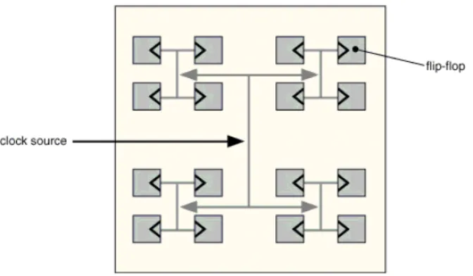
3.2.5 Clock tree synthesis
Post power network analysis, clock tree synthesis is performed. This task breaks
down the clock so as to reduce running of long metal wires in the chip. Buffers are
inserted in their path from source to destination to introduce delay for data
synchronization. This delay may be achieved with long metal wires too, but it introduces
a lot of unnecessary issues like parasitic effects during routing. Figure 3.3 below gives a
[image:46.612.150.486.388.584.2]idea of how clock tree buffers are inserted in this process.
which is usually around the range of pico-seconds. The clock skew can be reduced
effectively by increasing the number of buffers inserted in a design, but aiming at that
alone will result in long interconnect within the design and hence a lot of power is
dissipated [32]. Therefore, there has to be trade off when inserting buffers to obtain a low
clock skew. Beside power, another metric of importance is the delay which is a
consequence of interconnect with the increasing buffer insertion [33].Zero skew models
have also been developed. This can be used more effectively in a hierarchical flow, where
two zero skew modules can be put together to obtain a zero skew for the top-level module
in the clock tree optimization phase [38].
Buffers in clock tree synthesis introduce two types of skew. One of them is due to
the buffer delays and process variations, while the other is a source from unbalancing
buffer loads. A work around to this problem is to cluster the design into smaller blocks
where the buffer loading is distributed equally among all the clusters and then drive each
of these clusters with additional buffers with higher driving strengths [24].
3.2.6 Routing & routing optimization
The next subsequent step after synthesizing the clock tree is to route the design.
The design is first checked for any routing congestion that may have occurred as a result
of the previous steps. A course routing of the design is performed and is later optimized
to meet the specified constraints [15] [16] [18].
Due to the increased number of transistors in the design, higher clock frequencies
and additional physical effect considerations, the design is likely to face problems like
placement and routing enables early estimation of the metric details like congestion,
timing and area and lets the tool to better optimize the design with respect to these in the
physical implementation process [6].
Figure 3.4 depicts the physical design tool. The basic framework of the tool
shows that it takes in the synthesized netlist along with some logical and physical
[image:48.612.150.505.253.623.2]3.3. Extraction
Once the design is routed, it is important to extract the parasitic capacitances
along the routed design and check the design for timing with these included. Being a
Synopsys supported design flow; the Synopsys tool used for extraction is Star XT. Given
the fully routed design and the Milkyway library associated with it, this tool is capable of
extracting all the parasitics with a process file as a reference. This is shown in the figure
[image:49.612.141.461.275.471.2]3.5.
Figure 3.5 Extraction tool – Star Xtract
3.4. Static timing analysis
The Synopsys static timing analysis tool ensures a single, trusted sign-off solution
for timing, signal integrity, power and variation-aware analysis [30]. Figure 3.6 below
explains the different versions of Prime Time, the Synopsys tool for timing analysis and
its compatibility with the other tools. In this design flow, the gates netlist out of IC
delay format) file that contains the gate delays and interconnects delays of the design
with the parasitics taken into consideration. This output file may be used by the RTL
designer to back-annotate the timing delays in the design and obtain a vector file (VCD)
[image:50.612.136.478.191.491.2]to perform power analysis.
Figure 3.6 Static timing analysis tool – Prime Time
Above mentioned stages in the design flow with the low power techniques
incorporated formulate the standard digital design flow. The following section explains in
detail the UPF synthesis process and the various preparations required by the designer
3.5. UPF synthesis
UPF or the Unified power format is an industry wide power format specification
to implement lower power techniques in a design flow. Power becoming an important
factor in today's electronic systems, lead to a need to have a more systematic approach to
reduce power in complex designs.
The UPF deals with setting power domains in a design to achieve power
optimization. It defines both language format and simulation semantics for Power gating.
The UPF is compatible with Synopsys tools at every stage in the design flow. Creating
power domains in a design at the RTL level is usually a cumbersome task, but at the
synthesis level and the physical design level, the tool makes it a very feasible task in
terms of power optimization.
As the flow advances, UPF synthesis is a slightly different from the regular
synthesis as explained in section 3.1. One of the most important features when a UPF
flow is being created is the target libraries the design will be implemented with. Being a
multi-voltage design, this calls the need for power switches, level shifters and isolation
cells in the standard cell library.
Based on the different kinds of power management schemes, the use of special
Figure 3.7 UPF Special cells and Power reduction techniques
Figure 3.7 above explains the usage of different special standard cells based on
the UPF requirement of the designer.
Level Shifters are used when there is a low voltage domain to a higher voltage
domain crossing. A level shifter is not required when a signal crosses a higher voltage
domain to a lower voltage, it strength being sufficient to drive cells with lower power
supply. When a signal crosses from a lower voltage area to a lower voltage area, a level
shifter is placed in between the domains to boost the signal strength to be able to drive a
higher power supply standard cell or gate. Level Shifter cells are hence used whenever
other. These are hence used any kind of hierarchical placement of designs with power
gating and multi-voltage domains.
Power Switches are special standard cells that are incorporated in design during
synthesis. This enables a certain voltage area to switch between two voltage supplies
specified, or to switch between the “supply” and “OFF” state. The output of this cell
forms the main supply to that particular voltage domain. These are hence suited best for
power-gating enabled design.
Retention Registers are special UPF cells that are used to preserve any state
retention logic when a voltage domain is powered down. The logic retained in these
registers is used when that specific module is powered up again. These cells are used
when such an application is desired.
Every design is associated with power intent information based on which parts of
it will be in power ON mode or power OFF mode. The power intent specification also
contains the voltage information to enable a multi-voltage setup. Typically a maximum
usage of 2 voltages is suggested to be used, but otherwise the UPF allows the designer to
use as many as desired. The design gets complicated enough to handle the domains in a
two voltage design. As explained earlier, the UPF specifies power domains in a design
which can be set by the designer at RTL level or the physical design engineer in the
implementation phase. Setting them up in the RTL being a more difficult task, hence it is
preferred to specify UPF constraints when the design is ready for synthesis. The RTL
designer however still bears the responsibility to design a state machine for power
management in the design, generally referred to as the power controller module. This
the switches to the power domains. This module has ports such 'shut down' or 'sleep'
connected to the enable ports of the modules in the power domains to enable them and
disable them based on the power requirements.
The test platform used to demonstrate the standard low power design flow and the
UPF synthesis is a 32 bits MIPS RISC processor. A VHDL model of the design is
synthesized. Details of the design, low power implementations in the design, power intent
Chapter 4
Test platform
The design chosen to implement the basic top-down back-end digital design flow
is a 32-bit MIPS RISC processor. The VHDL model is synthesized, placed and routed.
The various components in the design are -
1. Instruction memory
2. Data memory
3. Register file
The design integrates the instruction and data memory as a single unit and makes
use of the address and data buses for control sequencing the instructions through the
various stages of its operation. The organization of the VHDL model for the processor is
as shown in Figure 4.1.
The flow is implemented in a systematic directory structure where the specific
scripts for the synthesis and placement are sourced from another exclusive scripts
directory. This can be better explained by a directory structure diagram that is used to
implement the flow. As shown in Figure 4.2 below, the top level directory is named as
the design to be synthesized or implemented, which in this case is the 32 bit MIPS RISC
processor. This top-level directory contains the directories of the main tasks to be
performed within it. Hence, there is a syn for synthesis, pnr for placement and routing,
star for parasitic extraction, and a sta folder to perform static timing analysis that have
common sub-directories namely in, out, report, and run. As the sub-directory name
suggests, each of them is formulated to hold their specific inputs, outputs and scripts to
of the design is performed under the 'syn' and the user can then perform the physical
design process on the design in the similar way under the 'pnr' directory and finally finish
[image:56.612.176.474.179.497.2]the signoff process to complete the flow.
Figure 4.2 Implementation directory structure
4.1. Top-down standard digital design flow
The design flow implemented is the same as explained in Chapter 3. The
top-down design flow consists of synthesizing the design using Design Compiler, importing
the netlist out of DC to ICC and performing the design planning, placement, clock tree
and routing processes on the design. Finally, parasitics are extracted from the routed
design using Star XT and timing analysis is performed using Prime Time and the design
with the layout is ensured to be clean from any sort of violations.
Each of these stages in the digital design flow is explained in detail with respect
to the RISC processor design and the constraints used on the design in the different stages
4.1.1 Synthesis of a 32-bit MIPS RISC processor
As discussed in Chapter 3, one of the main design requirements for synthesis is
the RTL description of the design. A VHDL model for the RISC processor is used by
Design Compiler to synthesize the design. The VHDL model description is shown in
Figure 4.1. The library used is a 65nm nanometer Synopsys provided standard cell
library. No special cell libraries are used for the standard top-down digital design flow. A
nominal voltage supply of 1.2V is used in this design, making the worst case voltage
1.08V and a best case voltage at 1.32V.
Besides the RTL and library information, it is very important to constraint the
design. In this case, an SDC (Synopsys design constraints) file is given to Design
Compiler which contains information about the design clocks, input delay and output
delay. For this RISC processor, there is one clock “CLK” that is constrained at 13.4ns or
approximately 74MHz. The design is then compiled until it is ensured that there are no
timing violations or errors when running the tool. Any of the constraints specified in the
SDC file is reported by synthesis. An area estimate is also reported after synthesis, which
may be used as a starting point during the design planning process of going further.
4.1.2 Physical implementation of a 32-bit MIPS RISC processor
As explained in Chapter 3, the physical implementation process of a design is an
elaborate procedure of design planning, placement, clock tree synthesis and routing.
this design, the maximum available routing layer is METAL9, minimum being METAL2.
The power rails designed in the design-planning process are usually the top 2 metal layers
available, leaving all the other layers convenient for routing. Therefore, METAL8 and
METAL9 are used to physically place the power rails VDD and VSS; they are designed
to run around the core of the die to ensure a minimum and acceptable IR drop. The core
area is set to ~0.2 sq.mm. (345 sq.µm in the X direction and the same in the Y direction).
The floorplan details and figures will be presented in results section- Chapter 5.
Once the design planning step is done in the GUI mode and the designer ensures
that it is the final floorplan for the rest of the flow, the floorplan can be written out to a
dump file that can called just before placement every time the flow is run. A detailed
placement is done as a consequent step to design planning. Placement optimization is also
done, it is very important to keep the placement utilization of the design within
acceptable levels. Placement utilization is the ratio of the standard cell placement to the
core area of the design. Typically, about 75% is a good start point and can go up to 90%
for complex designs. For this design, a utilization of 71% after placement was observed.
After placement of the standard cells, clock tree synthesis is performed. The tool
enables the user to provide a set of buffers and inverters to be inserted, and only these
will be used in the process. These cells definitely have to be available in the standard cell
library used by the design for synthesis and implementation. The placement utilization
generally is known to increase with the addition of the clock tree cells; the RISC
processor placement utilization observed was about 72%. Design being less complex and
almost minimum hold-time violations did not increase the utilization, but for a design
The design is then routed to obtain a fully implemented netlist. Specific routing
constraints can be set by the user depending on the complexity of the design. The routing
congestion map being in an acceptable form for the RISC processor, very limited routing
constraints were used. Finally, a netlist and a layout file (GDSII) for a fully routed design
are written out.
4.1.3 Extraction and Timing sign-off
The parasitics are extracted from a fully routed netlist using the StarXtract tool.
There exists a star.options file which contains the necessary Milkyway database
information of the design for which the parasitics have to be extracted. The parasitics file
is a .spef extension file that is used later for generating delay format files during timing
sign-off. The designer should ensure there are no hold/setup violations at the different
corners (slow and fast) after sign-off. PrimeTime enables the designer to write out delay
format files which may be used for power estimation later in the flow.
4.2. UPF synthesis (RISC processor)
The synthesis of the 32-bit MIPS RISC processor with the UPF incorporated is
explained in this section. Having explained the details of UPF in Chapter 3, it is quite
evident that the most significant start point of the UPF constraints is the power intent
information. This is a pictorial representation of the voltage domains in a design and its
different power modes as desired by the designer.
Figure 4.3 Power-Intent specifications for 32-bit MIPS RISC processor
As shown in Figure 4.3 above, 'mem_sw' is a power switch which shuts ON and
OFF the power domain 'POWER_DOWN'. Level shifters are also shown in the design, it
is very important to insert these level shifters when a signal in the design goes from a
lower voltage to a higher voltage, so that it will be able to drive the output at that point.
Retention registers are also special cells in the library that may be used. These are used in
a design when the output state of a module has to be restored after the module has been
shut down once and switched ON again. The 32 bit MIPS RISC processor uses power
<