Optical Properties of Capped Metallic
Nanostructures, Grown on Silicon
Niall McAlinden
06128394
Declaration
This thesis has been submitted to the University of Dublin for examination for the degree of Doctor in Philosophy by the undersigned.
This thesis has not been submitted as an exercise for a degree to any other uni-versity.
With the exception of the assistance noted in the acknowledgments, this thesis is entirely my own work.
I agree that the Library of the University of Dublin may lend or copy this the-sis upon request.
Niall McAlinden October 2010
Abstract
Reflectance anisotropy spectroscopy (RAS) is a linear optical technique that mea-sures the difference in the reflectance of two orthogonal polarisations at normal incidence. It achieves surface and interface sensitivity when the bulk material, such as a cubic semiconductor, is optically isotropic. The penetration depth of optical ra-diation allows RAS to probe buried interfaces. RAS has been used to probe various one-dimensional (1-D) structures grown on vicinal Si(111) surfaces under ultra-high vacuum (UHV) conditions. The RAS system response was extended into the IR, where important optical transitions occur, for both a photoelastic modulated sys-tem and a rotating sample syssys-tem using a tuneable IR laser. RAS spectra of single domain Si(111)-5×2-Au, Si(557)-Au and Si(775)-Au structures showed large min-ima in the region around 2 eV and, in the case of Si(111)-5×2-Au a large maximum below 1 eV.
The monolayer (ML) coverage of Au required for the Si(111)-5×2-Au surface reconstruction has been extracted from the RAS response. Using the well known coverage of Au required for the Si(557)-Au reconstruction, the Au deposition rate was accurately calibrated. By analysis of the coverage required for several Si(111) vicinal off-cuts, taking into account the different step densities, a coverage for a ”pure” Si(111)-5×2-Au surface was calculated. A value of 0.59 ML± 0.08ML was found, in agreement with the recent work. The value supports a new three chain model for the Si(111)-5×2-Au surface reconstruction.
Upon deposition of small amounts of Si adatoms on the Si(111)-5×2-Au surface and subsequent annealing, the RAS spectra changed dramatically, as the adatom decorated ”5×4” reconstruction was formed. Temperature dependent studies al-lowed 100% and a 0% adatom filled sites RAS spectra to be extracted. These spectra will be particularly useful for comparison with future ab initio optical re-sponse calculations. The optical signatures from this surface could prove to be very interesting in the study of defect induced charge density waves.
The RAS response from Si(557) shows two peaks related to surface modified bulk states at 3.4 eV and 4.25 eV, and a surface state at 1.2 eV. The RAS signal was compared with preliminary ab initio optical response calculations. Reasonable results were found for a bulk terminated and relaxed Si(557) surface. However, the structure is known to consist of a triple step structure of approximately (112) orientation and the large terrace of the Si(111)-7×7 reconstruction. Calculations of the RAS spectra from Si(112) did not reproduce the features seen experimentally.
Acknowledgments
First and foremost I would like to thank my supervisor Prof. John McGilp. He worked closely with me throughout the four years of my thesis, giving advice and guidance when needed. He always encouraged discussion and debate within the group which lead to a great working environment. I will miss the weekly coffee meetings where new results and ideas were shared and openly talked about.
I would also like to thank Dr. Conor Hogan for all the computational results on the Clean Si(557) surface. When he was told that I was submitting in 4 months he rose to the challenge, read up on a surface he had not studied before, worked through several problems with the code and in the end produced some nice results. I wish him all the best with the Gold modified Si(111) surfaces.
The IR-RAS results would not have happened without the help of Dr. Jing-Jing Wang. He helped setting up the DFG laser and always had good advice on alignment of the optics.
The whole group who I have worked with over the last 4 years all have had an input into this work. Lee and Julie for showing me the basics of UHV, and sample mounting and cleaning. Karsten for introducing me to the RAS system. John for helping me any time the UHV system was acting up, Lina for always giving a helping hand with the laser and Chris for his help with the optical analysis of almost everything. As with any thesis there are countless others who have had an input so I hope I don’t forget anybody; Cormac, Nikos, Brian, Declan, Dannel, Martin, Iggy, Ming, Nina, Rugerro and the many summer and 4th year students that have come through the group in the four years I’ve been here.
I am very grateful of all the support I have received from the electronics and mechanical work shops in the school of physics. Nigel deserves special credit for getting everything back working after a flood in the lab in 2008. Joe, Dave, Mick, and Ken have also provide valuable help and advice during this thesis. And thanks to John Kelly for always making me laugh and solving any problems I asked him to. No thesis would be possible with out all the help and encouragement received from outside of physics, I would like to thank my family, my mum and dad, Rita and Harry, and my sisters, Ciara and Amy and all my friends who ran, cycled, swam or drank (some who did all four) with me throughout the four years. I would like to especially thank the Triathlon club in Trinity for introducing me to so many new friends.
Publications
R. Verre, K. Fleischer, S. Sofin, N. Mc Alinden, J. F. Mc Gilp, and I. V. Shvets. In situ characterization of one-dimensional plasmonic Ag nanocluster arrays. Phys Rev B, Accepted Jan 11, 2011.
N. McAlinden and J.F. McGilp. New evidence for the influence of step morphology on the formation of Au atomic chains on vicinal Si(111) surfaces. EPL, 92, 67008, 2010.
N. McAlinden and J.F. McGilp. Using surface and interface optics to probe the capping, with amorphous Si, of Au atom chains grown on vicinal Si(111). Journal of Physics: Condensed Matter, 21(47): 474208-13, 2009.
List of acronyms
0-D 0-Dimensional 1-D 1-Dimensional 2-D 2-Dimensional
AES Auger Electron Spectroscopy AFM Atomic Force Microscopy a-Si Amorphous Silicon CDW Charge Density Wave
DFG Difference Frequency Generator DFT Density Functional Theory FTIR Fourier Transform Infrared
GW Greens function and screened interaction IR Infrared
l-N2 Liquid Nitrogen
LDA Local Density Approximation LEED Low Energy Electron Diffraction ML Monolayer
MLWA Modified Long Wavelength Approximation MOKE Magneto Optical Kerr Effect
OPA Optical Parametric Amplifier PBN Poly-Boron Nitride
PEM Photo-Elastic Modulator
RAS Reflection Anisotropy Spectroscopy RegA Regenerative Amplifier
RFA Retarding Field Analyser SDW Spin Density Wave
SEM Scanning Electron Microscopy STM Scanning Tunneling Microscopy STS Scanning Tunneling Spectroscopy TE Thermoelectric
UHV Ultra High Vacuum UV Ultraviolet
List of element abbreviations
Ag Silver Ar Argon As Arsenide Au Gold Ba Barium C Carbon Ca Calcium Cd Cadmium Cu Copper F Fluorine Ga Gallium H Hydrogen Hg Mercury In Indium K Potassium Mg Magnesium N Nitrogen Na Sodium O Oxygen Pb Lead
Pr Praseodymium Si Silicon
Contents
Declaration . . . i
Abstract . . . ii
Acknowledgments . . . iv
Publications . . . v
List of acronyms . . . vi
List of element abbreviations . . . vii
1 Introduction 1 1.1 Opening remarks . . . 1
1.2 Scope of the thesis and overview of the literature . . . 3
2 Physics in one dimension 7 2.1 Properties of metals in 1-D . . . 7
2.1.1 1-D density of states . . . 7
2.1.2 Peierls instability . . . 8
2.1.3 Charge density waves . . . 9
2.1.4 Ballistic electron transport . . . 10
2.1.5 Spin-Charge separation . . . 10
2.1.6 Fermi contours, a measure of 1-D character . . . 11
2.2 Examples of 1-D systems . . . 13
2.2.1 Bechgaard salts . . . 13
2.2.2 Conducting polymers . . . 13
2.2.3 Carbon nanotubes . . . 14
2.2.4 Wires grown by the vapour liquid solid method . . . 15
2.2.5 Wires pulled using a break junction method . . . 15
2.2.6 Metals on stepped semiconductor surfaces . . . 16
3 Experimental Details 20 3.1 Sample preparation . . . 20
3.2 Molecular beam epitaxy . . . 23
3.3 Low energy electron diffraction and Auger electron spectroscopy . . . 25
3.4 Scanning electron microscopy . . . 26
4 Reflection Anisotropy Spectroscopy 28 4.1 Rotating sample/polariser RAS . . . 29
4.3 Origins of a RAS spectrum . . . 37
5 Si(111)-5×2-Au and related surfaces 41 5.1 Early work . . . 41
5.2 Development of a structural model for Si(111)-5×2-Au . . . 41
5.3 Faceting . . . 45
5.4 RAS results and discussion for Si(111)-5×2-Au . . . 45
5.4.1 Si(111)-5×2-Au RAS signal . . . 46
5.4.2 Si(111)-5×2-Au coverage . . . 47
5.4.3 Annealing temperature dependence on the formation of Si(111)-5×2-Au . . . 49
5.4.4 Adatoms on Si(111)-5×2-Au . . . 51
5.4.5 Capping of Si(111)-5×2-Au . . . 56
5.4.6 Comparison with previous work . . . 58
5.5 The Si(775)-Au reconstruction . . . 58
5.5.1 RAS results and discussion for Si(775)-Au . . . 59
5.5.2 Ad-atoms on Si(775)-Au . . . 60
5.5.3 Capping of Si(775)-Au . . . 61
5.6 The Si(557)-Au structure . . . 61
5.6.1 RAS results and discussion for Si(557)-Au . . . 63
5.7 Summary . . . 65
6 Ab initio calculations of the optical response of Si(557) and Si(775) 67 6.1 Details of the calculations . . . 68
6.2 Results . . . 69
6.3 Predicted optical spectra . . . 70
6.4 Conclusions . . . 74
7 Metallic nanoislands 75 7.1 Growth of nanowires by anisotropic diffusion . . . 75
7.1.1 Silver islands . . . 75
7.1.2 Lead islands on Si(557)-Au and Si(335)-Au . . . 75
7.2 Modeling the optical response from metallic nanowires . . . 76
7.2.1 Anisotropic Drude free electron model . . . 78
7.2.2 Anisotropic polarisability . . . 79
7.2.3 Image charge model . . . 85
7.2.4 Anisotropic dipole-dipole interactions . . . 86
7.3 RAS from Pb islands grown on Si(557)-Au . . . 90
7.3.1 Uncapped islands . . . 90
7.3.2 Capped islands . . . 91
7.3.3 SEM images from Pb wires grown on Si(557)-Au . . . 94
7.4 Fitting of the RAS results to the model . . . 95
7.4.1 Fitting the RAS spectra from Pb islands . . . 96
7.4.2 Fitting the RAS spectra from Ag islands grown on Si(111)-3×1-Ag . . . 98
7.4.3 Limitations of the different models . . . 100
7.5 Summary . . . 100
8 Conclusions and future work 102 8.1 Overview . . . 102
8.2 Outlook . . . 103
A Jones matrices 105
B FlexRAS LabView Program 106
C Excel fitting worksheet 110
1
Introduction
1.1
Opening remarks
[image:12.595.204.422.269.485.2]As modern industry drives for ever smaller and faster electrical components they encounter both physical and processing limitations. The physical problems in some cases are related to strange new physics due to the reduced dimensionality of the structures [1]. For example Ag nanodots (∼ 20 atoms) grown on Si(111)-3 × 1-Ag (figure 1.1) [2, 3] are not metallic, but are semiconducting [4]. The processing limitations are related to the difficulties in actually producing features that are smaller than∼30nm.
Figure 1.1: Ag Nanodots on a Si(111)-3×1-Ag (after [4]).
These nanostructures have a high surface to volume ratio. A 1 cm cube of Ag contains about 6×10²² atoms. Of these 7×10¹⁵ are surface atoms, or 1 in 107. In the silver nanodots the 20 atoms are in a single atomic layer, so they are all surface atoms. This problem is unavoidable, but with some clever device design these strange properties can be used to make devices that are faster than conventional electronics [5]. However, if the surface of the device is changed it can drastically alter the properties of the device. This is a major problem as exposure to the ambient will drastically alter the surface of most materials. To avoid these issues structures are often grown under ultra high vacuum (UHV) conditions at pressures≤ 10−10 mbar. Structures can then be capped with a material to prevent the corrosion and contamination by the ambient on removal from the growth chamber.
the structures have been altered in any way. Conventional surface science techniques, like scanning tunneling microscopy (STM), atomic force microscopy (AFM) and low energy electron diffraction (LEED), work extremely well with uncapped nanoscale systems, but due to the low penetration depth of electrons they cannot be used to study capped nanostructures. However, photons have a large penetration depth (figure 1.2). This means that optical techniques can ”look under” the cap and provide important information about the properties of buried structures, provided the signal can be distinguished from the underlying bulk [6–9]. In addition, electrical conductivity can be measured optically [10], thus avoiding the contact problem when characterising nanostructure conductivity.
Figure 1.2: A comparison of escape depth between optical and electron based tech-niques (after [9]).
wave-length light or electrons but it is unclear what resolution this will be able to achieve in practice. A way around this problem is to use a technique called self-assembly or bottom up production [13]. This is when nanostructures grow themselves. An example of this is deposition onto a stepped surface. Generally, the most energet-ically favorable position for adatoms to sit is at the step edge [14]. This method can even produce single atomic chains which are very interesting model systems for 1-dimensional (1-D) physics [15] (chapter 2).
The main optical technique that was used during this project to study nanoscale surfaces and interfaces was reflection anisotropy spectroscopy (RAS), a linear opti-cal technique. It uses symmetry to achieve surface and interface selectivity. RAS measures the difference in reflectivity between two orthogonal polarisations at near normal incidence and thus can be used to study surfaces and interfaces with in-plane optical anisotropy [16]. If the bulk is isotropic only the surface will produce a signal. A comprehensive review of RAS has been published recently [17]. Two different experimental set-ups were used. The first technique used a photo-elastic modulator PEM to effectively switch the polarisation of the light at a frequency of 56 kHz. The other technique used a sample rotation stage that spun at 20 Hz. Both techniques have advantages and disadvantages depending on the spectral range [18]. A detailed discussion of RAS is included in chapter 4.
1.2
Scope of the thesis and overview of the literature
The scope of this project is to produce and characterise wires grown by self-assembly that are less than 10 nm in two of their dimensions and then to investigate how capping changes their properties. Physics ofquasi 0-, 1- and 2-dimensional material is an exciting area of research and with new processing techniques it has become possible to create systems that are at the limits of a single atom [19], single atomic chain [20] or single atomic layer (monolayer, ML) [21].
Figure 1.3: A simplistic picture of a vicinal surface, whereα is the vicinal angle. In the example drawn, Si(775), the angleαis∼8.5◦ in the [112] direction. The dotted line represents the optical surface.
When grown on singular Si(111) these systems are multi-domain, because each of the 3 surface domains that are rotated from each other by 120◦ have equal energy of formation. For large area probes, including RAS, macroscopic averaging will result in an overall 3-fold symmetry, hiding the lower symmetry of the individual domains. Vicinal substrates cut close to the [111] direction (see figure 1.3) can produce perfectly aligned step structures with suitable heat treatment [27, 28] (figure 1.4) . Deposition can then lead to a single domain, as the domain aligned with the steps generally has a lower energy of formation [29].
Figure 1.4: Step array on a Si(111)-7×7 surface. The image contains a single kink in about 20,000 step edge sites; the location is highlighted by the red square. The image is 340× 390 nm. (after[28]).
Another method of producing 1-dimensional structures is to deposit on a sub-strate that has a strong anisotropic diffusion. Atoms can diffuse in one direction only and long metallic islands can be formed. Two examples of this type of growth are Ag deposited on Si(111)-3×1-Ag [7] and Pb deposited on Si(557)-5×1-Au [39]. Various attempts have been made to model the infrared (IR) optical anisotropy of these metallic structures including an antenna model [40], anisotropic Drude dielec-tric model [7] and a Bruggeman type model [41]. These models are discussed further in chapter 7.
2
Physics in one dimension
One dimensional (1-D) physics has captivated theoretical physicists for generations. Many problems can be solved analytically in 1-D that do not have an analytical solution in higher dimensions. While a true 1-D material is purely a theoretical construct several materials approaching 1-D can now be routinely manufactured in the lab. These materials have hinted at some strange new properties of materials, such as exotic types of superconductivity and unusual quasi-particles. It is very important that these materials are understood and hopefully new technologies will emerge due to their unique properties.
2.1
Properties of metals in 1-D
In two and three dimensions electrons can easily avoid each other but in 1-D they can’t and become strongly correlated. This implies that the single electron Fermi liquid model for weakly interacting electrons is no longer adequate and must be replaced by models involving collective excitations, such as the Tomonaga-Luttinger liquid model [43, 44]. Even without considering these collective excitations, physics in 1-D will be drastically different to physics in higher dimensions, as the next four sections outline.
2.1.1 1-D density of states
In solid state physics, the density of states of a system is the number of states at each energy that are available to be occupied. The density of states is related to the curvature of the bands at that particular energy. The flatter the curvature the greater the density of states. For a 3-D free electron metal the density of states is given by:
g(E) dE = 1 2π2
2m
¯
h2
3/2√
E dE (2.1)
whereg(E) is the density of states andm is the mass of the electron. For a 1-D free electron metal the density of states is drastically different and is given by [45]:
g(E)dE = 1 2π2
2m
¯
h2 1/2
X
i
niH(E−Ei)
(E−Ei)1/2
dE (2.2)
where H is the Heaviside step function (H(x) = 0 when x is negative, H(x) = 1 when x is positive). Ei is the onset energy for each energy level and ni is the
Figure 2.1: The 3-D free electron gas density of states compared to the 1-D free electron gas density of states
while 1-D density of states shows a series of spikes called van Hove singularities. These van Hove singularities are important in optical spectroscopy as they will give strong absorption spikes at energies where an electron can be promoted from one van Hove singularity to the next. They will also show strong fluorescence as electrons decay down from one singularity to the next. This 1-D density of states behavior has been recorded for single wall carbon nanotubes [46].
2.1.2 Peierls instability
Figure 2.2: A schematic of the Peierls instability. a) A half-filled parabolic band structure for a 1-D chain of electrons. b) The same chain after a periodicity doubling along the chain direction, which induces a back-folding of the band structure with a band gap opening. The light gray shaded area shows the energy gain associated with the transition.
if the metallic chain is supported on a substrate, such as Si, this transition can be suppressed due to the interaction of the chain with the rigid lattice of the substrate, and will only be seen at very low temperatures. The transition between room temperature Si(111)-4×1-In and low temperature Si(111)-8×2-In is an interesting example of the complexity of Peierls transitions in surface structures [48–51].
2.1.3 Charge density waves
wave (SDW) where the spin will be sinusoidally modulated in space. SDW are seen in several 1-D materials such as Bechgaard salts [56–58] and high Tcsuperconductors
[59]. They have also recently been predicted to occur on Si(553)-Au and Si(557)-Au [60], but have not been observed.
2.1.4 Ballistic electron transport
Ballistic transport is the motion of electrons with negligible electrical resistivity due to scattering through the material. It occurs for materials where the mean free path of the electron is significantly greater than the length of the wire containing the electron. When this happens the resistance in the wire will depend solely on the contact resistance. The contact resistance Gc can be calculated and is a universal
constant for a 1-D conductor. The number of transverse modes in the wire is given by N = 2W/λf where W is the width of the wire and λf is the Fermi wavelength.
Each mode can carry a current of Im = Ve2gmυm where V is the voltage between
the two ends of the wire,e is the charge of an electron,gm is the density of states of
the mode and υm is the group velocity of the mode. The group velocity is related
to the density of states by gm = 1/(¯hυm). Substituting into the previous equation
gives:
Im =
e2 ¯
hV (2.3)
As new modes are introduced the conductance will jump in steps of 2e2/¯h(the factor of two is introduced because each mode can carry two electrons, one up-spin and one down-spin). This result has been shown experimentally for several different types of samples [61–63].
2.1.5 Spin-Charge separation
Figure 2.3: Two models of spin-charge separation. a) The delocalised Tomonaga-Luttinger liquid model predicts that a partially filled band will split into a spinon and holon band, that are degenerate at the Fermi level. b) The localised Hubbard model gives a clearer picture of what is happening, and consists of a antiferromagnetic array of electrons. When a hole is created by photoemission a neighboring electron can hope into it, in this case causing the hole to move to the left. This leaves two electrons of equal spin beside each other creating a spinon (after [15]).
carbon nanotubes [66, 67], indium atomic wires [68] and chains of PrBa2Cu4O8 [69]. The evidence for non-Fermi electron gas behavior comes from the width (lifetime) of angle resolved photoemission transitions [70].
2.1.6 Fermi contours, a measure of 1-D character
The Fermi surface of a crystal structure is an abstract boundary in reciprocal space, marking the boundary between the filled and empty electron states. Its shape de-pends on the periodicity and symmetry of the crystalline lattice, and on the electron density, which determins the length of the Fermi vector. Figure 2.4 shows the Fermi surface for a 3-D noble metal.
Figure 2.4: The Fermi surface for a perfect face centered cubic noble metal. It consists of a sphere with necking points, where the sphere will be in contact with neighboring spheres.
2.2
Examples of 1-D systems
Material scientists have been able to produce a large variety of inorganic and organic compounds, which exhibit highly anisotropic electronic properties and effectively behave as 1-D conductors. They range from organic polymers to superconductors. Some of these materials are discussed here and, where their anisotropic optical properties have been studied, these will also be discussed.
2.2.1 Bechgaard salts
Bechgaard salts were discovered in 1979 by Klaus Bechgaard [72]. They showed superconductivity at very low temperatures and had highly anisotropic conductivity at room temperature. They consist of a tetrathiafulvalene building block (figure 2.6) which is a planar molecule. In a crystal the tetrathiafulvalene molecules will stack and inorganic ions can form chains between the stacks. They show several instabilities as they are cooled and can form both CDWs and SDWs. Reflection properties of some of the Bechgaard salts have been studied both along the stack direction and perpendicular to it, but not with RAS [56, 58, 73]. These reflectance properties show a huge anisotropy, equivalent to a RAS signal of ≥500, although it is a bulk effect compared to the surface effect seen on metallic chains on Si surfaces. The reflectance measurements were carried out from the far IR to the visible (0.001 eV to 2 eV) and were able to detect details about the metal-to-insulator CDW transition that occurs at around 100 K [73] and metal to insulator SDW transition that occurs at around 10 K [56, 58]. Details about the vibrational modes in the salt were also studied. Bechgaard salts normally have a intrachain to interchain coupling strength of ∼10 indicating that they still have significant 2-D/3-D character.
Figure 2.6: The main building block for a Bechgaard salt. When the molecules are crystalised they stack leaving channels where the cations can sit and form long conducting chains.
2.2.2 Conducting polymers
con-ducting polymers in the year 2000. They have the potential to combine the positive properties of polymers, such as ease of processing, flexibility and elasticity, with electrical conductivity. They also show some 1-D metallic properties, as they have much greater conductivity along the polymer chain than perpendicular to it. How-ever, there is significant interchain interaction, which suppresses the formation of a truly 1-D metal. Conducting polymers show a temperature behavior more like a disordered metal than a true 1-D conductor [74]. In some systems, where the poly-mer is made into thin wires∼30 nm in diameter, CDW have been seen and can be used to create interesting switching devices [75]. Reflectance and absorption studies have been completed on some conducting polymers [76, 77] and have given some new insights into the metal-to-insulator transition that is observed at high doping levels.
2.2.3 Carbon nanotubes
Figure 2.7: Predicted RAS signal from aligned single wall nanotubes, data was taken from [81].
2.2.4 Wires grown by the vapour liquid solid method
The vapour-liquid-solid (VLS) growth method involves growing very thin nanowires by depositing droplets of metal onto a substrate, then increasing the vapour pressure of the material to be deposited. The metal acts as a nucleation site/catalyst for the material and long wires are produced with a diameter roughly equal to the size of the original droplet [82]. This method produces long wires aligned vertically from the substrate and, because of this geometry, no reflectance spectra have been published for light polarised parallel and perpendicular to the wires. The properties of these wires can be quite different from the bulk material. For example, Si nanowires with a diameter of around 2 nm depending on the crystallographic orientation of the wire may have a direct band gap [83]. Technologically, this is a very promising approach. This method, however, is currently limited to wires of ≥ 2 nm, which means that they do not show significant 1-D metallic properties.
2.2.5 Wires pulled using a break junction method
Figure 2.8: Schematic of two STM break junctions a double atomic wire (left) and a single atomic wire (right). The wires are created by crashing a STM tip into a metallic surface and slowly withdrawing it (after [86])
looses a conduction path, for example going from a triple to double atomic wire or a double to a single atomic wire. This phenomena is called quantised conductance and is related to ballistic conductance discussed previously. The field is dominated by the creation of Au wires [63, 84] but other metals such as Fe and Cu have also been studied [85]. These short wires are surprisingly stable and will survive different ambient conditions including liquids and atmospheric pressure. They can survive incredibly high current densities due to the ballistic conduction of electrons through the wire. Instabilities are seen in these wires and they can never be more than a few atoms long before breaking. However, they provide some very interesting test systems. Agrait et al have published a comprehensive review of the topic of break junctions [63]. Optical properties of these wires would be extremely difficult to study as the wires are created individually. It may be possible in the future to create arrays of these wires using a method similar to that of Kiguchi et al [84], allowing their optical properties to be studied.
2.2.6 Metals on stepped semiconductor surfaces
received most attention, due to the relative ease by which it can be produced and the vast array of possible stepped Si(111) surfaces, is the Si(111)-Au system. Aspects of this system are discussed extensively in chapter 5 and so only some details of the surfaces will be given here.
Si(111)-5×2-Au is an extensively studied, but controversial system which consists of a double or triple chain chain of Au atoms and a stable Si honeycomb chain on a Si(111) surface [24]. The surface is decorated with Si adatoms that sit on top of the chains in a 5×4 lattice [36, 55]. Only about 50 % of the lattice sites are ocupied and the surface segregates into regions covered with adatoms and regions without adatoms. From angle resolved photoemmision (ARPES) results it has been established that the covered regions are semiconducting with a band gap of about 0.6 eV and the uncovered regions are metallic [55, 87]. The adatoms appear to cause a CDW to form on the chains in a similar manner to the defect mediated CDW formation on the Si(553)-Au surface [88] or the absorbate induced CDW that is formed when Na is deposited on Si(111)-4×1-In [89]. The optical response of Si(111)-5×2-Au is discussed in detail in chapter 5.
The Si(557)-Au system has received a lot of attention due to the paper by Segovia
SDW is thought to form on the step edge [60]. The RAS spectra from Si(557)-Au are discussed in detail in section 5.6.
The Si(553)-Au system has received a lot of interest in the last 5 years [96]. This reconstruction forms when 0.48 ML of Au is deposited on the clean Si(553) surface [97]. The structure consist of two Au chains running parallel to the step edge [98]. The surface has 3 fractionally filled bands (called S1, S2 and S3) that cross the Fermi energy. The surface shows some wiggling in the Fermi contours, indicating that there is significant interchain coupling. Two of the bands that cross Ef are spin-orbit spit
bands, S1 and S2, similar to Si(557)-Au. It is thought that the third band, S3, is related to a row of unsaturated dangling bonds on the terrace [53]. When this surface is cooled several distortions are seen. STM images show a ×3 periodicity along the step edge and a ×2 periodicity on the terrace [53]. LEED images show a ×3 periodicity indicating a lattice distortion, but this has not been confirmed [53, 71]. four point probe measurements clearly show a metal to insulator transition occurring at around 150 K [71]. Defects in this system have a profound effect on the the CDWs seen in STM. Their transition temperature and their correlation length are affected, and the defects can pin CDW fluctuations [88, 96]. Reproducibility in this system is difficult to achieve and analysis of results becomes difficult. A SDW has also been predicted to form on this surface at low temperature [60], but has yet to be confirmed experimentally. RAS spectra from Si(553)-Au have not been recorded, however the Si(775)-Au surface, which has a similar structure to the Si(553)-Au surface [70], is discussed in section 5.5. The main differences between the two reconstructions will be a greater interchain interaction for the Si(553)-Au surface compared to the Si(775)-Au surface [30].
Figure 2.9: RAS spectra from Si(111)-4×1-In at room temperature and at 80K, after [105]
3
Experimental Details
3.1
Sample preparation
All of the samples produced during the course of this work used commercially avail-able vicinal off-cuts of Si(111) as the substrate. Si(111) has two stavail-able off-cut di-rections, [11¯2] and [¯1¯12] [23, 28]. Unreconstructed steps in the [11¯2] direction have 1 dangling bond per step atom while steps in the [¯1¯12] direction have 2 dangling bonds per step atom (figure 3.1). This affects the stability of each of the surfaces. The step density of the surface also affects its stability. Highly unstable surfaces will tend to facet if kinetics allow them to. This means that steps will bunch and the surface will have large step-free terraces [109, 110]. In order to use stepped surfaces as templates for producing single domain surfaces, it is essential to start with regu-lar step arrays which exhibit atomically straight step edges and low kink densities. Samples are cleaned by firstly degassing at 600◦C for several hours until the pressure is below 10−10 mbar and then flash heating a number of times to 1200◦C in ultra high vacuum (UHV) [109, 111]. UHV is defined in this work as a pressure below 10−10 mbar.
Figure 3.1: This figure shows two steps on unreconstructed Si(111), the right hand step is towards the [11¯2] direction, the left hand step is towards the [¯1¯12] direction. The steps towards the [11¯2] direction have a single dangling bond per step atom while steps towards the [¯1¯12] direction have two dangling bonds per step.
Figure 3.2: The sample mount used for UHV experiments. The green pieces are tantalum, the gray pieces are Al2O3 and the orange piece is the Si sample.
a filament and accelerated by an electric field to high energies to heat a sample by transfer of kinetic energy on collision. A third method, used in this work, involves passing a high current through the sample, called resistive heating. In the case of Si the resistive heating method is the most convenient because Si, like all semi-conductors, has a negative thermal coefficient of resistance. This means that as Si gets hotter its conductance goes up due to an increase in thermal charge carriers. The first stage of resistive heating is to apply a high voltage across the sample to breakdown the native oxide layer and to create enough thermal carriers for current to begin flowing. When a current is established the sample can be uniformly heated from around 150◦C to its melting point. It is important for these experiments that the current always flows parallel to the steps on the Si(111) surface. If the current flows perpendicular to the steps it can cause electromigration of the steps and step bunching will result [112–114]. Each sample can go through several cleaning cycles but eventually the sample degrades due to microscopic roughness called blooming.
Samples are mounted in UHV using a simple clamp (Figure 3.2). Current can then be passed through the sample by applying a voltage between the terminals marked positive and negative.
Figure 3.3: The emissivity of Si. The green region are the wavelengths detected by the high temperature pyrometer and the yellow region are the wavelengths detected by the low temperature pyrometer (after [115]).
For the low temperature pyrometer this is not the case. Also, there is another complication with the low temperature pyrometer. A special UHV MgF2 window must be used for this pyrometer, as fused silica will absorb in its wavelength range. To get around these problems a calibration curve was established using a platinum resistor attached to the back of a Si sample. This platinum resistor could read in the range from -50◦C to 800◦C but was destroyed by heating above 800◦C and so could not be attached to the sample during sample cleaning. The emissivity on the pyrometer was fixed at 0.1 and the recorded temperature could be converted into a real sample temperature. The errors associated with pyrometry are relatively large and with the calibration curve they become larger again. The error on the high temperature pyrometer was established to be ±20◦C while on the low temperature pyrometer the error was ±50◦C.
Figure 3.4: RAS spectra of clean Si(557): The structure marked at 4.25 eV is only seen when the surface is clean and well ordered.
were confirmed using low energy electron diffraction (LEED) and Auger electron spectroscopy (AES) (section 3.3). However, it was found that RAS could act as a good fingerprint method to confirm that the surface was clean and well ordered (figure 3.4).
3.2
Molecular beam epitaxy
a) b)
Figure 3.5: a) Schematic of the HTEZ-40 from MBE-Komponenten. b) Schematic of the SUSI from MBE-Komponenten
background pressure of ∼ 5×10⁻¹⁰ mbar. A Si Sublimation Source (SUSI) from MBE-Komponenten (figure 3.5b) was used for the evaporation of Si for capping studies on Si(111)-Au and Si(557)-Au-Pb systems. The SUSI allowed growth of high quality ultra-thin Si layers. It provided a very clean (background pressure of 1×10⁻⁹, this background pressure was confirmed to be H2 using a quadrapole mass spectrometer) and constant Si flux. The SUSI is commonly used for Si-doping of GaAs epilayers in MBE growth facilities. The specially designed free standing silicon filament arch is directly heated by electrical current up to 50 A and is surrounded by high purity silicon shielding parts. Heating of metal and ceramic parts is minimised by very effective water cooling of the electrical contacts. No insulating ceramic parts are used in the hot zone.
Table 3.1: Evaporation temperatures and evaporation rates. Metal Temperature Approximate deposition rate Au 1200◦C 0.0002 ML s−1
Pb 650◦C 0.01 ML s−1 Si >1200◦C 0.011 ML s−1
Figure 3.6: LEED image, viewed from the rear, taken from the clean Si(111)-7×7 surface.
3.3
Low energy electron diffraction and Auger electron
spec-troscopy
Low energy electron diffraction (LEED) is an electron based technique for deter-mining the surface structure of crystalline materials [118]. It has surface sensitivity due to the low penetration depth of electrons in the region from 10 eV to 200 eV (figure 1.2). LEED can provide detailed measurements of surface atomic position by monitoring the spot intensity as the beam energy is scanned [119]. However, LEED was used in this project purely to confirm well ordered surfaces. A LEED image is an image of the reciprocal lattice of the surface. Figure 3.6 is an example of a LEED image from a clean Si(111)-7×7 reconstructed surface. On ordered stepped surfaces spot splitting is sometimes seen, but on the low angle off-cuts that are used in this work spot splitting was not seen due to the large terrace width and low coherence length of the electron beam
Figure 3.7: Schematic of the LEED-Auger system. To change from LEED to AES the inner grids are switched to an oscillating retarding field and the drain current from the screen is measured with a lock-in amplifier.
atom spacing and they have a very small inelastic scattering mean free path, giving surface sensitivity. A schemitic of the LEED/AES system is shown in figure 3.7.
Auger electron spectroscopy (AES) is a complimentary technique to LEED which can be used to study surface composition and monitor the cleanliness of a surface. Auger electrons are emitted from an atom as it relaxes after a core electron has been ejected. They have a unique energy spectrum for each atom and are used to determine the chemical composition of the surface.
Both LEED and AES were carried out using the same apparatus, an Omi-cron SpectaLEED rear view LEED/AES system (figure 3.7). It consists of a front mounted electron gun, four high transparency grids, and a phosphor screen. For AES experiments the grids are switched to an oscillating retarding field the drain current on the screen was measured, this type of apparatus is called a retarding field analyser (RFA).
3.4
Scanning electron microscopy
Figure 3.8: SEM image of Pb nanoislands on a Si(557)-Au surface.
through focusing optics to create a very small spot. The electrons are scattered off the surface of the material being imaged and into a electron detector. A resolution of ∼1 nm can be achieved using a 30 keV beam. This resolution is limited by the electron beam radius. To prevent charging effects samples must be in good electrical contact with earth. This is archived using conducting carbon tape to hold the sample to the manipulator. Images are analysed using special software to extract average length and width of islands. An example of a SEM image of Pb nanoislands is shown in figure 3.8.
4
Reflection Anisotropy Spectroscopy
Reflection Anisotropy Spectroscopy (RAS) is a versatile optical technique. It mea-sures the difference in reflectance between light polarised in orthogonal directions in the surface plane (∆r) at near normal incidence, normalised by the mean reflectance
r. The RAS signal can be simply described by: ∆r
r =
2(rx−ry)
rx+ry
(4.1) where rx and ry are the complex Fresnel reflectance coefficients for light polarised
in the x and y direction respectively. RAS can achieve surface and interface sensi-tivity in systems where the bulk is isotropic and the surface or interface is optically anisotropic.
RAS was first described by Aspneset aland Berkovitset alin 1985 [16, 120]. This early work was mainly interested in the study of III-V semiconductors [120, 121] and the recently discovered high temperature superconductors [122]. It was understood early on that RAS had the potential to be a quick and cheap method of studying growth of III-V semiconductors [18, 123–128] because it could operate in environ-ments where electron based techniques could not [129]. However, in recent times RAS has found applications in a broad range of material systems. These include clean single crystal metals [130–135] and semiconductors [16, 136], self-organisation of organics on surfaces [137, 138], surface reconstructions [139–141], aligned nanos-tructures on surfaces [4, 6, 7, 38, 142, 143] and systems which have been strained along one axis [144–147] (figure 4.1).
At present there are no standard methods for interpreting RAS spectra. With the advent of more powerful supercomputers, RAS spectra can be calculated from first principles. When RAS spectra are analysed from first principles they can provide quite strict limits on the surface structure. Small differences in surface structure can lead to significant changes in the band structure near the Fermi level. As any direct optical measurement probes both the ground and excited state additional computational power is required to calculate optical spectra compared to techniques which only prob the ground state. It is well known, for example, that the widely used density functional theory (DFT) approach significantly underestimates the band gap of semiconductors. However, if these problems can be overcome, RAS can be used to confirm one structural model ahead of others, as has been shown recently for the Si(111)-4×1-In surface [25].
meth-Figure 4.1: The dependence of the RAS signal as Si(100), an isotropic surface, is strained along the [001] direction is shown here. The maximum strain reached before the sample broke was 3.9×10⁻⁴.
ods, mechanical rotation of the sample or polarisation and photoelastic modulator (PEM) switching of the polarisation. The most common is now the PEM method, as it offers the opportunity of excellent signal to noise due to the high modulation frequency. During the course of this project a rotating sample setup and 2 PEM instruments were developed.
4.1
Rotating sample/polariser RAS
The simplest way to measure a RAS spectra is to rotate the polarisation of the light with respect to the sample. In this sense both sample rotation and input polarisation rotation are equivalent. For this discussion the Jones matrix formalism will be used (see appendix A). Under the Jones formalism the reflectance of the sample can be described by:
rx 0
0 ry
!
(4.2)
If we assume a rotating input polarisation given by:
E0eiφcosωt
E0eiφsinωt
!
where ω is the rotational frequency of the input light, the output after reflection from the sample is given by:
rxE0eiφcosωt
ryE0eiφsinωt
!
(4.4)
The magnitude of this vector squared then gives the signal recorded at the detector (V ∝I ∝E2, whereV is the voltage on the detector,I is the intensity andE is the electric field)
V ∝|rx |2 cos2ωt+|ry |2 sin2ωt (4.5)
This can be rewritten as:
V ∝ |rx | 2 +|r
y |2
2 +
|rx |2 − |ry |2
2 cos 2ωt (4.6)
In this equation (|rx |2 +|ry |2)/2 can be replaced by R and|rx |2 − |ry |2 by ∆R
giving:
V ∝R+∆R
2 cos 2ωt (4.7)
This means that there are two components of the signal, a DC component and a component at a frequency of 2ω. By measuring both of these components the RAS signal can be extracted
V2ω
V0
= ∆R
2√2R (4.8)
To show that a rotating sample gives a similar response, the condition that a component with Jones matrixM rotated by θ about the x axis can be represented by a new Jones matrix M(θ).
M(θ) = R(−θ)M R(θ) (4.9)
R(θ) is given by:
R(θ) = cosθ sinθ −sinθ cosθ
!
(4.10)
A sample rotating at a frequency ofω has a Jones matrix:
rxcos2ωt+rysin2ωt (rx−ry) cosωtsinωt
(rx−ry) cosωtsinωt rxcos2ωt+rysin2ωt
!
(4.11)
With linear input polarisation this gives an output Jones vector:
rxcos2ωt+rysin2ωt
(rx−ry) cosωtsinωt
!
Figure 4.2: A rotating RAS set-up. The sample is rotated at a frequency ofω.
which neatly simplifies to equation 4.5 by again using trigonometric identities. Hence the measured signal can again be described by equation 4.8.
(Coherent, RegA 9000) and the seed beam was from a optical parametric amplifier (OPA) (Coherent, OPA 9800) which is tunable in the region from 1.3 eV to 0.54 eV. The laser has a bandwidth of∼12 nm which means that a monochromator was not needed. The lasers have a pulse width of ∼ 200 fs and the pulse frequency is 100 kHz. The I0 signal is replaced by I100kHz which can be detected with a good
signal-to-noise using a lock-in amplifier. Spectra were recorded by first tuning the laser to the desired energy, then recordingI2ω and I100kHz up to 100 times in about
3 minutes. An average of these points was taken and the RAS signal was calculated. The program for reading from the lock-in was written in LabView. It consisted of the following logic:
1. Set time constant.
2. Set the Lock-in to read 100kHz 3. Set to 1st harmonic.
4. Wait 5 times the time constant. 5. Read the signal at 100 kHz. 6. Set the Lock-in to read atω
7. Set to 2nd harmonic
8. Wait 5 times the time constant. 9. Read the signal at 2ω.
10. Repeat from 2. until the required number of points has been recorded.
4.2
Photoelastic modulator RAS
To avoid the problems associated with a mechanical rotation a PEM can be used. A PEM is a device that modulates the phase of the light in one optical axis (hence changing the polarisation state of the light). It is essentially a dynamic waveplate. It works by applying an electric field to a piezoelectric crystal which is coupled to a suitable transparent material, such as quartz or CaF2. The piezoelectric induces a stress in the material which changes its birefringent properties. Light polarised along the modulation axis will undergo a phase modulation of Γ, while light polarised perpendicular to the modulation axis will be unchanged.
Γ = Γ0sinωt (4.13)
not just the real part as in the rotation (intensity modulation) experiments discussed in section 4.1.
In the Jones matrix formulation a PEM can be described by: cosΓ2 isinΓ2
isinΓ 2 cos
Γ 2
!
(4.14)
If an experiment is constructed such that the PEM axis and input polarisation are at 45◦ to the anisotropic axis of the sample, the amplitude of the electric field output (A) is proportional to:
A∝ cos
Γ
2 isin Γ 2
isinΓ2 cosΓ2
!
rx 0
0 ry
!
1 1
!
∝ rxcos Γ
2 +irysin Γ 2
rycosΓ2 +irxsinΓ2
!
(4.15)
This would produce a phase modulation at the detector. In order to turn the phase modulation into an intensity modulation an analyser polariser is used, at 45◦ to the PEM axis (parallel to the sample axis). This means the amplitude at the detector is:
A∝ 1 0
0 0
!
rxcosΓ2 +irysinΓ2
rycosΓ2 +irxsinΓ2
!
∝ rxcos Γ
2 +irysin Γ 2 0
!
(4.16)
The voltage on the detector is proportional to |A|2, and is a harmonic series of V0,
Vω, V2ω etc. By performing a Fourier transform we find that each term depends on
a Bessel functionJn, where n is the order of the Bessel function. Odd harmonics are
found to depend solely on the imaginary part of ∆r/r while even harmonics depend solely on the real part of ∆r/r:
Vω
V0
∝ J1(Γ0)Im(∆rr) sin(ωt) (4.17)
V2ω
V0
∝ J2(Γ0)Re(∆rr) cos(2ωt) (4.18)
V3ω
V0
∝ J3(Γ0)Im(∆rr) sin(3ωt) (4.19) The PEM RAS system, as well as giving excellent signal-to-noise and access to both real and imaginary parts of the RAS signal, allows us to perform some very simple calibration measurements. If the input polariser is misaligned with respect to the PEM axis there will be a constant offset in the signal. This can be used to check for nonlinearities in the PEM or other components.
Figure 4.3: A schematic of a PEM RAS system, after [17].
Both systems are of a similar design (figure 4.3). The broad band system consists of a high pressure Xe lamp, MgF2 coated Al mirrors, a filter wheel, MgF2 Rochon polarisers, CaF2 PEM (Hinds instruments, II/CF57), a three grating monochro-mator (Bentham Instruments, TMc300-USB), a Si-InGaAs detector (Elektronik-Manufaktur Mahisdorf) and a liquid N2 (l-N2) cooled InAs detector (Hamamatsu). Detectors were changed using a micro stepper motor. The DC signal was read us-ing a sensitive analogue to digital converter and the AC signal was read with a lock-in with a reference frequency of twice the PEM frequency. The components that differed in the compact system are the polarisers (quartz Glan-Taylor), the PEM (fused silica) (Hinds instruments, I/FS50), there is no InAs detector and the monochromator had two gratings. A flexible LabView program was written to allow interchangeability between several different components and could be used with both systems. The program also allowed several types of measurement. These include spectral RAS, time dependent RAS (to monitor growth), magnetic field dependent RAS (essentially measuring the magneto optical Kerr effect, MOKE), PEM voltage dependent RAS (to calibrate the PEM) and alignment mode where the DC and AC signals are plotted for alignment of samples and other components. A description of the LabView code is included in Appendix B
Figure 4.4: The broad-band RAS system
1 mm2) area around the electrodes, which means the focal size can also be small. Even though the Xe is at high pressure the lamp still produces strong emission lines, especially around 1.2 eV (figure 4.5). Intensity is limited in the IR and UV mainly because of light being absorbed in the bulb material.
Focusing and beam alignment in the RAS systems was performed using MgF2 coated Al mirrors. These mirrors have a good reflectance over a large spectral range and are resistant to corrosion. They offer ≥90% reflectance from 3 eV to 0.12 eV, and a ≥ 85% reflectance from 5 eV to 3 eV. The main focusing mirror had a focal lenth of 1 m for both systems, which alowed the beam to be directed through a low strain quartz window into the vacuum chamber. A secondary focusing mirror was used to focus into the monocromator.
MgF2 Rochon polarisers were used in the broad band system. They separate the light into two beams with an angular separation of about 3◦, varying slightly with wavelength. They have an extinction ratio of at least 10−5 and work in the region from 9 eV to 0.2 eV. On the compact system quartz Glen-Taylor polarisers were used. They are crystals cut close to Brewster’s angle so that the refracted and reflected beams are polarised. The refracted beam has an extinction ratio better than 10−5. They work in the region from 5.5 eV to 0.6 eV.
Figure 4.5: The emission from a high pressure Xenon bulb
the PEM using LabView it is possible to use it from 5 eV. This PEM modulates the light at 57 kHz. The PEM for the compact system is made from fused silica and is optimised in the region from 5 eV to 1.5 eV. Again by using a calibration and LabView this range can be extended to 1 eV easily and 0.75 eV if a damping factor is included. The PEM on the compact system operates at 50 kHz.
The monochromator and filter wheel select the energy of the light. The monochro-mator for the broad band system has 3 gratings, one for ≥2.1 eV, one for 2.1 eV to 0.8 eV, and the 3rd for ≤0.8 eV. Under normal conditions the slit width on the monochromator is 1 mm, giving resolutions of 1.35 nm, 5.4 nm and 10.8 nm re-spectively, for the different energy ranges. The filter wheel is used to prevent 2nd order effects in the monochromator. There are 4 filters for different energy ranges. A neutral density filter was also incorporated to help prevent detectors overloading in the region of the strong lamp lines. For the compact system a much smaller monochromator is used. It consists of two gratings, one for above 3 eV and one for 3 eV to 0.75 eV. Due to the small size of the monochromator the resolution is much poorer than the broad band system, a resolution of∼10 nm is recorded on the first grating and∼25 nm is recorded on the second grating.
to split the DC and AC signals, which were then connected to the analogue to digital converter and lock-in, respectively. To switch between these two detectors a micro stepper-motor was used. The signal cables into the lock-in were switched using solid state relays. There was a small damping of ∼ 5% of the AC signal coming from the InGaAs detector. The third detector was an InAs liquid N2 cooled detector. It was designed to work in the region from 0.75 eV to 0.42 eV. It was shipped with a filter on the signal line that damped the AC signal by a factor of ∼10000, but the lock-in could still read an AC signal, albeit with significantly more noise than the Si and InGaAs detectors. This problem was resolved by recording the AC several times and using a long time constant. Recording a much higher density of points in the region of this detector and post measurement averaging of points also helped. The detectors on the compact system were the same as the Si-InGaAs detectors on the broadband system.
4.3
Origins of a RAS spectrum
The optical transitions probed by RAS are determined by both the bulk and surface dielectric function of the material. To be useful for surface science RAS must be sensitive to the surface structure of the material at the atomic scale. This can be achieved if the bulk crystal is isotropic. For cubic and amorphous materials it is clear that there is no bulk anisotropy so any RAS signal must come from the surface. Unreconstructed (111) and (100) surfaces of cubic materials are isotropic and show no RAS signal, however the (110) surface is anisotropic and will have a RAS signal (figure 4.6). Reconstructed (111) or (100) surfaces from cubic materials can give a RAS signal but normally they will be in a number of equivalent domains, and domain averaging will mean no RAS signal is recorded. This is because RAS will sample over a macroscopic area due to the size of the beam spot and domain averaging will mean no RAS signal is seen.
The Jones matrix method explains how different experimental set-ups can detect small anisotropies in the reflectance from a sample, but the question of where this anisotropy comes from has not been addressed. Phenomenological models have been developed to relate the optical anisotropy to the surface dielectric function.
The 3 phase model assumes a sample consisting of an isotropic bulk (with di-electric function b), thin anisotropic surface layer (xs and ys) and then a vacuum
Figure 4.6: RAS signal from two different (110) surfaces of cubic materials, Si and Au.
differential reflectance measurements: ∆r
r =
4πid λ
xs −ys b−1
(4.20) where d is the thickness of the anisotropic layer, λ is the wavelength of the light,
b is the bulk dielectric function of the substrate and is is the dielectric function
of the surface layer in the i direction. While equation 4.20 is useful as it relates ∆r/r to ∆ it still does not explain where the anisotropy originates. A number of different phenomenological models have been used [17]. These include a Lorentzian describing an optical transition that is only active when light is polarised in one direction (equation 4.21), a surface modified bulk state [139, 149, 150] (equation 4.22) and anisotropic conductivity [10] (equation 4.23). During the course of this work a model involving a Bruggeman type dielectric function was also developed for large anisotropic metallic islands (section 7.2.2). The formula used are:
Lorentzian;
xs = 1 + S/π
ωt−ω+iΓ/2
y
s = 1 (4.21)
where S is the amplitude, ωt is the energy of the transition and Γ is the full width
at half maximum height (FWHM); Surface modified bulk state;
∆s ≈(∆Eg−i∆Γ)
db
where ∆Eg and ∆Γ are the relative shifts in energy and line width for x and y polarisation; Anisotropic conductivity; ∆r r = 2d 0c ∆σ b−1
(4.23) where ∆σ is the difference in optical conductivity between thex andy directions of the surface.
Each of these models give some phenomenological understanding of the physics underlying the RAS spectra, however in many cases none of these methods will suffice and sometimes more than one method is required, depending on the spectral region. A first principles approach is necessary for a fundamental understanding of RAS spectra. Optical measurements have always been a challenge to calculate. Until the late 1990s most RAS calculations used an empirical adjustment so that the experimentally measured band gap matched the calculated gap [151, 152]. However, this approach is clearly limited [153].
An optical transition in the visible or near IR region of the electromagnetic spectrum involves the excitation of an electron from its ground state to an excited state above the Fermi level. In order to calculate an optical spectrum from first principles both states must be accurately described and the matrix element linking them must be calculated. Within the independent particle model the imaginary part of the dielectric function is given by:
Im[M(ω)]∝
X
v,c
Z
BZ
|hϕv,k|qi|ϕc,ki|2δ(∈c − ∈v −¯hω)dk (4.24)
where M(ω) is the frequency dependent dielectric function, ϕv,k is a function
de-scribing the valance band, qi describes the matrix element linking the valance and
conduction band and ϕc,k is a function describing the conduction band.
Density functional theory (DFT) is currently the main approach for electronic structure calculation and is a very good method for calculating the ground state properties of a system [154]. Calculations can be made in a reasonable time frame by using the local density approximation (LDA). This assumes that the contribution to the exchange correlation, arising from the electron density at a certain distance, is equal to that of a homogeneous electron gas with the same density.
repeated in the surface normal direction. Molecular dynamics calculation are often used to adjust the atomic positions in the surface region to obtain a minimum in the potential energy of the system prior to calculating the optical response.
The optical properties of a system are expressed through its dielectric function. To calculate this both the valance band and conduction band should be known (equation 4.24). The error in the conduction band energies associated with DFT are often corrected by using a rigid band offset based on the experimental bulk values. For Si, this correction is ∼ 0.6 eV [155]. Quite small adjustments in the atomic positions can have drastic effects on the predicted RAS spectra, showing that RAS can be an extremely useful surface structure probe [25]. In the 1960s a new method of calculating the exchange correlation energy was described, called the GW approximation[156]. It is computationally very expensive, but the development of high performance computing has allowed the GW approach to be used to produce much more satisfactory calculation of optical properties of surfaces. For a bulk system the GW correction has a similar effect to the rigid band offset, but for surfaces it leads to a non-uniform shift in optical transition energies, producing a change in RAS line shape as well as shifting the spectrum.
5
Si(111)-5
×
2-Au and related surfaces
5.1
Early work
[image:52.595.169.450.394.611.2]Initial studies involving Au deposited on Si single crystals were trying to find out if Au was a suitable dopant for microelectronic components [163, 164]. These ex-periments gave some interesting results and similar systems involving Si nanowires are still studied today as potential solar cell materials [165, 166]. During the course of these early studies it was found that Au would form different surface reconstruc-tions depending on the thickness of the Au layer. Figure 5.1 shows a surface phase diagram of these reconstructions. The lowest coverage reconstruction was found, by Bishop and Riviere in 1969, to be a ”5×1” reconstruction [167]. For the next decade studies on this ”5×1” surface were concerned with discovering its structure [168]. An assumption was made that the Au was simply weakly absorbed on an unperturbed Si(111)-1×1 surface. It was not until an experiment by Perfetti et al in 1980 that it was discovered that the surface layer was in fact Si rich [169], leading to new models where the Si(111)-1×1 surface was perturbed.
Figure 5.1: Surface phase diagram of the Si(111)/Au system (after [170]).
5.2
Development of a structural model for Si(111)-5
×
2-Au
em-Figure 5.2: Si adatoms on top of Si(111)-5×2-Au. The bright white spots are the Si adatoms (after [36]).
bedded in the surface layer [169]. However, there is still debate about the structure of this widely studied system. Even the Au coverage is controversial [98].
Early structural models relied on X-ray standing wave measurements [171, 172] and low energy ion scattering [173] to determine atomic positions. These early experiments identified that the Au was embedded in the 1st atomic layer of the Si(111). The studies also showed that the Au was in an unusual site. On Si(111) there are three common bonding sites identified, a 6-fold coordinated site in between layers of Si(111) and a 1- and 3-fold coordinated site above the surface plane. The Au sat in none of these sites [172, 174].
When atomic resolution STM images were recorded in the early 1990s they should have helped resolve the surface structure but instead they added more compli-cations. Images of the Si(111)-5×2-Au were covered in bright spots of high electron density, labeled protrusions (figure 5.2) [33, 175, 176]. Initially these protrusions were labeled as Au adatoms [177] because the two chain model of the 5×2 reconstruction required ∼0.4 Ml of Au but it was always found that the optimum reconstruction was formed at slightly higher coverages, often above 0.5 ML [38, 178]. By accounting for one adatom per two 5×2 unit cells this meant that the optimum coverage for Au would be ∼0.45ML, a better agreement with experiment. However, when these adatoms were identified as Si [36], the coverage discrepancy was largely ignored.
[image:53.595.207.411.67.305.2]confirmed both experimentally [36] and theoretically [35]. It was discovered that the adatoms are key to the stability of Si(111)-5×2-Au. They sit on a site between two Au chains and form a 5×4 superlatice [24, 35, 37, 54, 179]. The adatoms will act as an electron donor for the chains, causing them to change from metallic to semiconducting. The mechanism of the band gap opening is not due to the indi-vidual adatom but more to a collective change in the structure of the chains on the surface [55, 180]. The adatoms drive a pseudo Peierls transition causing a doubling of the periodicity along the chain direction and subsequent band gap opening. The coverage of one adatom per two 5×2 unit cells is not normally observed over the whole surface. The as deposited coverage is about one adatom per four unit cells. The surface segregates into two regions, adatom-free 5×2 and adatom-decorated 5×4 (figure 5.2). The reason behind this segregation are unclear but it is thought to relate to the hopping potential of adatoms between neighboring sites and the relatively low binding energy of the Si adatoms [54, 181]. It is possible to saturate all the adatom sites by depositing Si onto the Si(111)-5×2-Au [55]. By annealing the surface to various temperatures the adatoms can then be removed.
Figure 5.3: Si honeycomb chain.
5.3
Faceting
Surfaces will normally reconstruct to minimise their surface free energy, and one way for them to do this is to pair up dangling bonds and form surface reconstructions (such as Si(111)-7×7 [184]). Another way is to rearrange surface atoms so that, instead of one high energy surface, two lower energy surfaces are formed. This was first discussed by Herring in 1951 [110]. For singular Si(111) this does not occur, but when steps are introduced it has been found that the steps will bunch at certain temperatures, forming facets. When Au is deposited on the surfaces it can change the faceting behavior drastically [175, 185–189].
Two examples of this Au-induced faceting are described. Si(111) off-cut in the [11¯2] direction, after appropriate heat treatment (section 3.1), will consist of equally spaced single height steps (figure 1.4), but when Au is deposited at 600◦C the surface changes into Si(111)-5×2-Au and Si(775)-Au facets [175, 185, 186]. Clean Si(557) will facet into (¯1¯12) triple height steps and Si(111) terraces with a doubled 7×7 reconstruction. The step and terrace forms a repeating structure that is 5.73 nm wide [116, 117]. When Au is deposited at 600◦C the surface reorganises into a perfect Si(557)-5×1-Au surface [188].
5.4
RAS results and discussion for Si(111)-5
×
2-Au
RAS spectra were recorded for Au deposited on Si(111) samples off-cut in both the [¯1¯12] direction and [11¯2] direction at various vicinal angles. Si was then deposited on top of the 5×2 reconstruction to firstly examine the effects of adatoms on the surface and then, after further deposition, to see if the electronic structure was significantly perturbed by the capping process.
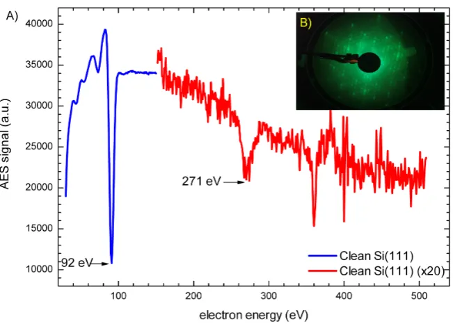
Clean surfaces were obtained by the procedure described in section 3.1, and LEED images and Auger spectra were recorded. Substrates were, n-type, doped with P, and had a typical resistivity in the range 1-10 Ω cm. The Auger spectra (figure 5.5 A) clearly show the large Si peak at 92 eV. By examining the spectra carefully in the region between 150 eV and 520 eV a residual carbon peak can be seen at 271 eV and no oxide peak can be seen (an oxide peak would be expected around 500 eV). Allowing for the AES cross-section and the response of the RFA, ∼ 0.02 ML of C is present on the surface. The LEED image shown in figure 5.5 B shows the 7×7 reconstruction associated with clean Si(111).
Figure 5.5: A) AES of clean Si. B) LEED of clean Si(111), showing the 7×7 reconstruction.
and 4.25 eV. These peaks are a step modified bulk signal which has an anisotropy due to the aligned steps [190]. It was found in general that the peak at 4.25 eV, was only seen on a clean well-ordered surface. Due to the relative simplicity of recording a RAS spectra compared to Auger and LEED, normal procedure was to clean the Si until the peak at 4.25 eV was optimised. Figure 5.6 shows a typical limit of RAS sensitivity of∼2×10⁻⁵, although the zero line error may be an order of magnitude larger.
5.4.1 Si(111)-5×2-Au RAS signal
Figure 5.6: RAS of clean Si(111) off-cut by 2◦ in the [¯1¯12] direction. This RAS spectra also shows the limit of the sensitivity of the RAS setup: the structure at 2.2 eV is related to a large change in the DC signal when the grating is changed and the structures at 1.2 eV and 1.4 eV are related to emission lines from the xenon lamp.
tail in metallic nanostructures [10]. LEED and Auger were used to confirm that a Si(111)-5×2-Au surface had been formed (figure 5.8). As well as the Si and C peaks seen on clean Si(111), peaks are seen at 45 eV, 56 eV and 72 eV, which correspond to Au.
5.4.2 Si(111)-5×2-Au coverage
Figure 5.7: RAS of Si(111)-5×2-Au off-cut by 2◦ in the [¯1¯12] direction.
![Figure 1.1: Ag Nanodots on a Si(111)-3 × 1-Ag (after [4]).](https://thumb-us.123doks.com/thumbv2/123dok_us/1685808.121972/12.595.204.422.269.485/figure-ag-nanodots-on-a-si-ag-after.webp)
![Figure 1.2: A comparison of escape depth between optical and electron based tech-niques (after [9]).](https://thumb-us.123doks.com/thumbv2/123dok_us/1685808.121972/13.595.109.513.273.532/figure-comparison-escape-depth-optical-electron-based-niques.webp)
![Figure 5.1: Surface phase diagram of the Si(111)/Au system (after [170]).](https://thumb-us.123doks.com/thumbv2/123dok_us/1685808.121972/52.595.169.450.394.611/figure-surface-phase-diagram-the-si-system-after.webp)
![Figure 5.2: Si adatoms on top of Si(111)-5×2-Au. The bright white spots are theSi adatoms (after [36]).](https://thumb-us.123doks.com/thumbv2/123dok_us/1685808.121972/53.595.207.411.67.305/figure-si-adatoms-bright-white-spots-thesi-adatoms.webp)
![Figure 5.4: The three Au chain model for the Si(111)-5×2-Au (after [24]). Au atoms](https://thumb-us.123doks.com/thumbv2/123dok_us/1685808.121972/55.595.238.390.397.633/figure-au-chain-model-si-au-au-atoms.webp)
![Figure 5.6: RAS of clean Si(111) off-cut by 2◦ in the [¯1¯12] direction. This RASspectra also shows the limit of the sensitivity of the RAS setup: the structure at 2.2eV is related to a large change in the DC signal when the grating is changed and thestructures at 1.2 eV and 1.4 eV are related to emission lines from the xenon lamp.](https://thumb-us.123doks.com/thumbv2/123dok_us/1685808.121972/58.595.149.477.74.311/figure-direction-rasspectra-sensitivity-structure-thestructures-related-emission.webp)

![Figure 5.11: RAS spectra recorded on Si(111) sample off-cut by 4◦ in the [11¯2]direction after annealing at various temperatures.](https://thumb-us.123doks.com/thumbv2/123dok_us/1685808.121972/62.595.152.476.76.313/figure-spectra-recorded-sample-direction-annealing-various-temperatures.webp)
