Quantum modelling of
semiconductor gain materials
and vertical-external-cavity
surface-emitting laser systems
Christina B ¨uckers*,1, Eckhard K ¨uhn1, Christoph Schlichenmaier1, Sebastian Imhof2, Angela Thr ¨anhardt2,
J ¨org Hader3,4, Jerome V. Moloney3,4, Oleg Rubel5,6, Wei Zhang7, Thorsten Ackemann8, and Stephan W. Koch1
1
Department of Physics and Material Sciences Center, Philipps-University Marburg, Renthof 5, 35032 Marburg, Germany 2
Faculty of Natural Sciences, Chemnitz University of Technology, 09107 Chemnitz, Germany 3
Nonlinear Control Strategies Inc., 3542 N. Geronimo Ave., Tucson, AZ 85705, USA 4
College of Optical Sciences, University of Arizona, Tucson, AZ 85721, USA 5
Thunder Bay Regional Research Institute, Thunder Bay, ON P7A 7T1, Canada 6
Department of Physics, Lakehead University, Thunder Bay, ON P7B 5E1, Canada 7
Centre for Biophotonics, SIPBS, University of Strathclyde, Glasgow G4 0NR, Scotland, UK 8
SUPA and Department of Physics, University of Strathclyde, Glasgow G4 0NG, Scotland, UK
Received XXXX, revised XXXX, accepted XXXX Published online XXXX
PACS 42.55.Px, 42.60.Lh, 78.20.Bh, 78.55.Cr, 85.35.Be
∗Corresponding author: e-mail[email protected]
This article gives an overview of the microscopic the-ory used to quantitatively model a wide range of semi-conductor laser gain materials. As a snapshot of the cur-rent state of research, applications to a variety of actual quantum-well systems are presented. Detailed theory-experiment comparisons are shown and it is analysed how the theory can be used to extract poorly known ma-terial parameters. The intrinsic laser loss processes due to radiative and non-radiative Auger recombination are evaluated microscopically.
The results are used for realistic simulations of vertical-external-cavity surface-emitting laser systems. To ac-count for nonequilibrium effects, a simplified model is presented using pre-computed microscopic scatter-ing and dephasscatter-ing rates. Prominent deviations from quasi-equilibrium carrier distributions are obtained un-der strong in-well pumping conditions.
Copyright line will be provided by the publisher
1 Introduction The quantitative modelling of semi-conductor laser materials and their electronic excitations is of significant importance for the design and development of efficient and optimised semiconductor laser devices. The accurate description of the important system ingredients is particularly critical in modern microlasers, where the properties of the relatively small amount of gain material has to be well adapted to the specific microcavity. Exam-ples of current interest are vertical-external-cavity surface-emitting laser (VECSEL) systems also known as optically-pumped semiconductor disk lasers, which have recently emerged as a new class of semiconductor lasers [1–5].
They combine the advantages of a semiconductor gain medium with the solid-state-laser cavity design and allow for the extraction of a high-power, diffraction-limited cir-cular output beam [6, 7].
explicitly. The predictive capability of our model has been validated by experiments for various material systems with emission wavelengths from the ultraviolet and visible to the near- and mid-infrared, see e.g. [10–12].
The microscopically calculated optical properties of semiconductor gain materials may be used to analyse and design laser devices. Especially, in microcavity lasers the proper description of the intricate interplay of the cavity and the optical response of the active layers is essential. Employing the microscopic approach, main characteristics of the laser device such as emission wavelength, thresh-old behaviour or input-output power characteristics can be evaluated.
This article reviews the application of the microscopic model to a wide range of material systems used in VEC-SEL and other laser systems. After our theoretical ap-proach is briefly introduced (Section 2), we discuss some of the relevant properties of an (AlGaIn)As-based VEC-SEL system in Section 3. Emphasis is placed on the anal-ysis of the lasing performance and in particular, the po-tential and limitations of optical in-well pumping are as-sessed. In Section 4 the laser gain and loss properties of the (AlGaInAs)(AsSb)-based material family are investi-gated and the application potential of various designs is explored. Section 5 addresses the characterisation, the las-ing properties and disorder effects in the dilute nitride (GaIn)(NAs)-based material system. Furthermore, the suit-ability of our approach to extract critical structural param-eters through the analysis of spectroscopic measurements is demonstrated in Section 6 for a Ga(AsSb)-based system. Finally, nonequilibrium effects are discussed in Section 7 highlighting the impact of the pumping concept on the per-formance of VECSEL systems.
2 Theoretical approach Semiconductor laser de-vices are critically influenced by the optical response of the gain material so that any quantitative model requires a consistent quantum mechanical theory. For this purpose, we have developed a microscopic model enabling us to simulate the relevant electro-optical properties of semicon-ductor heterostructures in a consistent way. As the cen-tral part, the many-particle interactions are calculated ex-plicitly. Only the structural layout and material constants are needed as input, and we do not have to resort to phe-nomenological parameters such as dephasing and scatter-ing rates, linewidth enhancement factors and the like.
The starting point of our approach is the calculation of the single-particle bandstructure and the correspond-ing Coulomb and dipole matrix elements. These are used as input for the microscopic determination of the absorp-tion/gain, the photoluminescence, and the intrinsic laser loss processes. While absorption and photoluminescence investigations allow for an accurate characterisation of semiconductor heterostructures, the laser gain and loss properties are relevant ingredients for the final perfor-mance of the laser device.
2.1 Bandstructure For the computation of the single-particle eigenenergies and eigenstates in a semi-conductor heterostructure, we apply k·p-theory which is
based on a perturbation method [13]. If we consider III-V semiconductors such as (AlGaIn)As- or (AlGaIn)(AsSb)-based materials, the eigenstates of the quantum well may be developed in split-off, heavy hole, light hole and elec-tronic contributions, each spin degenerated. In this man-ner, the band structure information is contained in an 8×8 matrix, the so-called Luttinger matrix. However, for di-lute nitride (GaIn)(NAs)-based structures the matrix has to be extended to a 10×10 matrix (Section 5). The required material parameters for the bandstructure calculation are taken from the literature [14, 15]. Finally, from the single-particle wavefunctions, we determine the optical dipole and Coulomb matrix elements needed for the microscopic computations.
2.2 Absorption and laser gain In order to compute the absorption/gain, the semiconductor Bloch equations are solved in second Born-Markov approximation [16]. The equations describe the dynamics of the microscopic polarisations, i.e. the interband coherence at a certain mo-mentum, which couple to carrier densities present in the system. In most of our applications, the carriers can be as-sumed to be in quasi-equilibrium and thus in a Fermi-Dirac distribution. However, the general approach also allows us to study the impact of nonequilibrium situations which are addressed in Section 7. Summing up the microscopic quan-tities yields the macroscopic polarisation which gives the linear response of the material system to a light field.
In this manner, the refractive index change as well as the absorption/gain spectrum of a quantum well can be deduced. Since we calculate the many-particle corre-lations explicitly in second Born-Markov approximation, the homogeneous linewidth of the optical spectra is de-termined by quantum mechanical scattering equations in-cluding temperature, density, and spectral dependencies in a consistent way. Thus, phenomenological dephasing pa-rameters are not required and unphysical features such as absorption below the band gap, wrong amplitudes and in-correct line shapes are avoided [17]. Our microscopic ap-proach has proven to realistically simulate the optical prop-erties through many comparisons to experiments for a mul-titude of material systems, see e.g. [18].
2.3 Photoluminescence Spontaneous emission rates are calculated on the basis of the semiconductor luminescence equations [19], which include the equations of motion for the photon number in a given light mode and the photon-assisted polarisations. They have been derived similarly to the semiconductor Bloch equations, but involve the quantisation of the light field. As for the computation of the absorption/gain, it is essential to calculate the many-particle interactions explicitly since only the inclusion of the excitonic correlations ensures the correct line shape of the resulting luminescence spectrum of the quantum-well system.
If one wants to compare calculated and experimentally measured spectra of a VECSEL system, one has to take into account that the line shape of a photoluminescence spectrum detected at the surface of a VECSEL structure is modified by cavity effects. In order to account for the dielectric environment in such weak-coupling systems, we apply an approach based on the derivation of a filter func-tion [20] which leads to the enhancement or reducfunc-tion of the luminescence at certain wavelengths. If we multiply the filter function evaluated for the specific dielectric structure with the calculated emission spectrum of the isolated quan-tum well, we obtain the actually detected photolumines-cence at the surface of the structure.
2.4 Laser loss processes The performance of a laser device is influenced not only by the gain but also by the losses in the system. The material loss processes are typically classified into carrier recombination at de-fect states, spontaneous emission and Auger recombina-tion. The individual contributions of the various processes depend on the particular material system and the operating conditions such as temperature and carrier density. Often, the defect losses are negligible if one is dealing with high-quality materials. Hence, one is left with the radiative and Auger losses which we calculate microscopically.
The radiative loss rate is deduced by integrating pho-toluminescence spectra which are obtained by solving the semiconductor luminescence equations. Furthermore, our microscopic approach allows for the computation of the non-radiative Auger recombination rates. For this purpose, we solve scattering equations for the electron and hole dis-tribution functions [9], which are derived in the same for-malism as the semiconductor Bloch and the semiconductor luminescence equations.
Phenomenologically, the spontaneous emission is ex-pected to increase quadratically with the carrier density since two particles participate in the process. Auger scatter-ing involves three particles, thus their contribution is sup-posed to increase cubically with carrier density. Although this might be a good approximation below transparency when the carriers basically obey Boltzmann statistics, we find strong deviations with increasing carrier density as degenerate Fermi-Dirac distributions arise [9]. Thus, es-pecially in the density regime relevant for lasing in most VECSEL systems the phenomenological formulas fail. In
contrast, the microscopic theory enables us to predict the radiative as well as the Auger losses quantitatively for any lasing condition [9, 21].
Altogether, the microscopic evaluation of both the laser gain and the losses, supplemented by heat conduction and cavity waveguiding calculations allows for a systematic analysis of semiconductor laser devices. Thus, the main characteristics of the system such as threshold behaviour, gain saturation or lasing wavelength can be studied and the potential of the specific designs can be explored.
3 (AlGaIn)As-based VECSEL systems Well-established active materials for laser applications are (AlGaIn)As compounds. This material system is widely used as a gain element in VECSEL devices. As a specific example, we focus here on a design for a VECSEL operating at a wavelength around 850 nm [22–24].
Conventionally, the active material is pumped optically by an external laser diode via barrier states from which the excited carriers relax into the quantum wells, thus generat-ing the occupation inversion [25]. An attractive alternative could be the direct pumping of in-well states not only be-cause this would reduce the excess energy (quantum de-fect) of the photo-generated carriers, but also since this technique enhances the wavelength range of possible pump sources, e.g. one could use bright and inexpensive diodes at 800-810 nm [26].
In order to characterise and identify the relevant ingre-dients determining the performance of the VECSEL de-vice, we apply our systematic microscopic approach. To figure out design specifications of the structure, spectro-scopic measurements are analysed first.
3.1 Layout of the laser structure In a VECSEL de-vice light is amplified by semiconductor quantum wells which are embedded in a cavity built of a Bragg reflec-tor and an external outcoupling mirror which is aligned at a certain distance from the gain element. Here, we focus on a VECSEL structure intended to operate at an emission wavelength around 850 nm.
The Bragg reflector is grown on a GaAs wafer using 30 repeats of alternating AlAs and (Al0.18Ga0.82)As
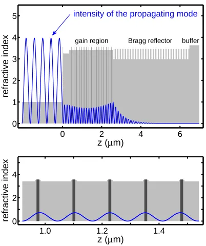
lay-ers which differ in their refractive indices as can be seen in the profile (Fig. 1, top). Each layer of the stack is de-signed to have the same optical thickness. Hence, a high-reflectivity stop-band centered at a wavelength of about 836 nm with a width of about 84 nm for normal incidence is established. On top of the Bragg reflector the active re-gion is deposited. It contains 17 (Al0.115Ga0.785In0.10)As quantum wells which are 10 nm wide and are surrounded by barrier layers made of (Al0.26Ga0.74)As. The quantum
intensity of the propagating mode
gain region Bragg reflector buffer
z (μm)
refractive index
0 2 4 6
0 1 2 3 4 5
z (μm)
refractive index
1.0 1.2 1.4
[image:4.612.68.269.98.338.2]0 2 4
Figure 1Top: Refractive index profile of the VECSEL struc-ture at a temperastruc-ture of 300 K (shaded area). The nominal structure consists of a resonant periodic gain region with 17 compressively strained (Al0.115Ga0.785In0.10)As quantum wells embedded in (Al0.26Ga0.74)As barriers grown on a 30-pair AlAs / (Al0.18Ga0.82)As Bragg reflector. The quantum well posi-tions are indicated in darker grey. The curve represents the inten-sity of the light field at a wavelength of 850 nm along the struc-ture. Bottom: Refractive index profile and intensity distribution of the laser mode within the resonant periodic gain structure.
strain effects which are caused by the different lattice con-stant of the quantum well material compared to the other layers of the structure. However, the band gap of the quin-ternary material is almost equal to that of the barrier layer, thus in the microscopic calculations we assume the quan-tum wells to be sandwiched between (Al0.26Ga0.74)As for
simplicity. Finally, an (Al0.50Ga0.50)As window layer and a Ga(As0.90P0.10) protective capping layer close the struc-ture. Further details on design and growth of the sample are given in [23].
All these different components in the structure lead to steps in the refractive index profile which substantially af-fect the optical properties of the VECSEL. In particular, the large jump of the refractive index from air to the front sur-face of the sample shows much higher reflectance than the semiconductor interfaces within the sample. Thus, a sub-cavity is formed between the sample surface and the front of the Bragg reflector. The resonant periodic gain structure defines a laser mode with a wavelength of about 850 nm, however this mode is not in resonance with the subcavity in the situation depicted in Fig. 1 because the mode
ex-hibits a node at the front surface of the sample reducing the light coupling into the structure.
3.2 Optical characterisation The analysis of spec-troscopic measurements by the microscopic theory allows for a detailed characterisation of the VECSEL structure. For this purpose, reflectance as well as photoluminescence investigations are carried out before building the laser cav-ity by aligning the external outcoupling mirror.
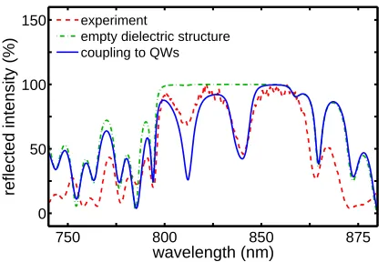
The reflectance spectrum of the sample measured at room temperature for normal incidence is plotted in Fig. 2 (dashed line). It is a result of interference effects of the light propagating and counter-propagating through the sample. In order to compute the reflectance and transmission at the boundaries of the dielectric structure, we employ the trans-fer matrix method. The required background refractive in-dices for the individual layers are extracted from the liter-ature [14, 27, 28] also taking into account the index disper-sion in the simulation. If we neglect the optical response of the quantum wells to the light field as a start, we find a flat high reflectivity stop band with adjacent interference features next to it (Fig. 2, dash-dotted line).
For a realistic description of the VECSEL structure it is crucial to include the active layers in the simulation. For this purpose, we pre-compute the wavelength-dependent optical susceptibility of the single quantum wells micro-scopically. The real part of the susceptibility determines the induced refractive index change in the quantum well layer and the imaginary part gives the absorption with its characteristic excitonic peaks. These spectra repre-sent a critical input to the VECSEL design and are ob-tained by solving the semiconductor Bloch equations for an (Al0.108Ga0.785In0.107)As / (Al0.26Ga0.74)As quantum
well in the low-density regime. The spectra are convoluted with a Gaussian distribution with a full width at half maxi-mum of 8 meV to account for growth inhomogeneities. The incorporation of the microscopically computed spectra in the transfer matrix calculation via wavelength-dependent complex refractive indices leads to a specific reduction of the reflectance at wavelengths where the quantum well ma-terial has absorption (Fig. 2, solid line). Due to the in-crease of intra-cavity losses in the excitonic resonances, two pronounced absorption dips arise in the stop-band at 812 nm and 840 nm which match the experimental obser-vation (Fig. 2, dashed line). The 840 nm dip is caused by the subcavity resonance coinciding with the excitonic res-onance induced by interband transitions between the first electron and the first hole subband.
wavelength (nm)
reflected intensity (%)
750 800 850 875
0 50 100
150 experiment
[image:5.612.59.272.99.243.2]empty dielectric structure coupling to QWs
Figure 2 Comparison of calculated (solid line) and measured (dashed line) reflectance spectrum of the VECSEL structure for normal incidence at a temperature of 300 K. In the simulation microscopically calculated low-density absorption spectra for the (Al0.108Ga0.785In0.107)As / (Al0.26Ga0.74)As quantum wells are included. If the optical response of the quantum wells to the light field is not taken into account, the dash-dotted line will be ob-tained.
our current studies and thus no optimisation attempts have been made.
As another independent method to characterise the VECSEL structure, we investigate the photoluminescence from the surface of the sample. The solutions of the semi-conductor luminescence equations are shown in Fig. 3 as dash-dotted line. The main peak at 840 nm arises due to transitions between the first electron and the first hole sub-band. Furthermore, there is a second signal at 812 nm cor-responding to higher-order interband transitions. To ac-count for the dielectric environment of the cavity we eval-uate the filter function (Fig. 3, inset). The product of this filter function with the microscopically calculated photo-luminescence of the isolated quantum well yields the sur-face emitted photoluminescence spectrum (Fig. 3, solid line). The comparison shows that the photoluminescence signals are more pronounced because of the spectral filter-ing. Both, the photoluminescence line shape as well as the spectral position agree well with the measurements (Fig. 3, dashed line).
3.3 Light amplification and laser loss properties
As soon as the VECSEL is pumped optically by an exter-nal laser diode, electrons are excited in the semiconductor structure. They relax to lower energies and occupy states near the band edge of the quantum-well material where they alter the optical response.
The characteristic dependence of the absorption spec-trum on the carrier density is depicted in the inset of Fig. 4 (top) for a single (Al0.108Ga0.785In0.107)As / (Al0.26Ga0.74)As quantum well at a temperature of 300 K.
Excitonic signatures corresponding to optically strong in-terband transitions brand the low-density spectrum, but with increasing occupation the peaks bleach out and
fi-wavelength (nm)
norm. photoluminescence
750 800 850 875
0 0.5 1
1.5 experiment
isolated QW QWs in laser structure
wavelength (nm)
filter function
800 825 850 0
0.5 1
Figure 3 Comparison of calculated (solid line) and measured (dashed line) photoluminescence spectrum of the VECSEL struc-ture for normal incidence at a temperastruc-ture of 300 K. In the sim-ulation cavity effects are taken into account by multiplying the microscopically calculated luminescence spectrum of the sin-gle (Al0.108Ga0.785In0.107)As / (Al0.26Ga0.74)As quantum well (dash-dotted line) with the wavelength-dependent filter function evaluated for the laser structure which is given in the inset.
nally, the absorption becomes negative in a spectral range near the band gap of the quantum well material and we enter the regime of optical gain.
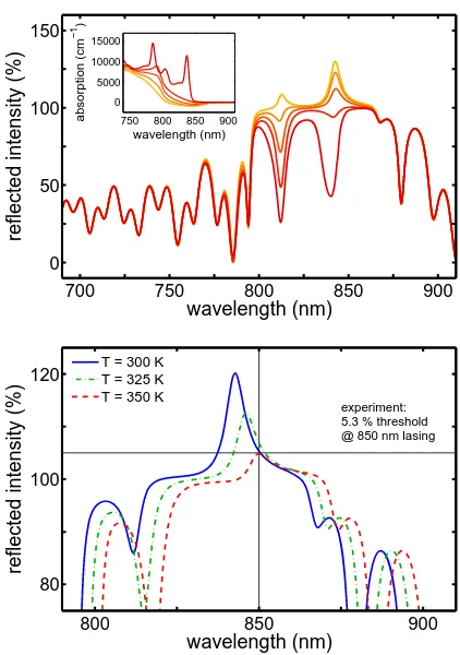
The microscopic results enter the transfer matrix cal-culation yielding the light intensity actually reflected by the VECSEL structure (Fig. 4, top). As soon as material gain is provided at the position of the cavity resonance, a narrow peak arises at 843 nm superimposed on the stop band. The peak is slightly red shifted relative to the ab-sorption dip obtained for low pumping because the cou-pling strength to the adjacent cavity resonance is modified. Obviously, the reflectance becomes larger than 100 %, i.e. the light intensity will be amplified by the system around the central wavelength. The amplification becomes more and more enhanced with increasing excitation due to the growth of the maximum of the underlying material gain spectra. However, a higher carrier density not only leads to a larger material gain, but also broadens the material gain spectrally. At a carrier density of 5×1012cm−2per quan-tum well transparency is already exceeded for wavelengths around the next energetically higher cavity resonance so that a second region of light amplification occurs around 813 nm. However, with regard to laser operation only the central peak is relevant defining a lasing wavelength of 843 nm at room temperature because this is the wavelength favored by the resonant periodic gain structure.
[image:5.612.314.522.100.243.2]out the calculations for a temperature of 350 K instead of 300 K, lasing at 850 nm is expected matching the experi-mental finding (Fig. 4, bottom). So we conclude a temper-ature increase of about 50 K in the active region which is a typical value for operating VECSEL devices reported in the literature [29].
The temperature increase results in a drop in amplifi-cation when the pumping power is kept constant. On the one hand, this trend is caused by the lower amplitude of material gain provided by the quantum wells as the carrier distribution smears out energetically with increasing tem-perature. On the other hand, with growing temperature the material gain shifts faster to longer wavelengths than the cavity resonance. For a temperature of 350 K the overlap of gain and cavity resonance is already strongly reduced. That is why one needs higher excitation densities to sus-tain a cersus-tain amplification level when the operating tem-perature increases. At 350 K we find a carrier density of 3.7×1012cm−2per quantum well required to achieve the lasing threshold of 5.3 % gain. This value is mainly deter-mined by the outcoupling losses, which are basically given by the reflectivity of the external mirror used to complete the laser cavity, and the internal losses of the laser.
From the engineering point of view, it is not only the carrier density which is important but also the pump intensity needed to sustain it. Hence it is crucial to study the loss processes in the semiconductor. Using our many-particle theory, the loss rate due to sponta-neous emission and Auger recombination is evaluated for an (Al0.108Ga0.785In0.107)As / (Al0.26Ga0.74)As quantum
well (Fig. 5). From the analysis we conclude that Auger processes play a minor role in this particular system com-pared to the radiative losses for the entire carrier density regime relevant for lasing. The recombination via defects is negligible. Since the VECSEL is expected to operate at about 350 K, the calculations are carried out for this perature. Compared to the results obtained at room tem-perature, the total loss rate is reduced by more than one order of magnitude. It is true, that the Auger rate increases with temperature, but more important for this material sys-tem are the radiative losses which become considerably lower because the probability of spontaneous emission is reduced due to the broadened carrier distributions for the higher temperature. However, the higher operating temper-ature also involves higher threshold carrier densities so that the benefits achieved by the reduced total laser losses are suspended.
3.4 Analysis of in-well pumping From the quanti-tative knowledge of the absorption, gain, and laser loss properties of the VECSEL structure the pump power nec-essary to achieve a certain amplification can be estimated by equating the carrier generation rate needed to sustain the gain against recombination. As discussed in Section 3.3, a carrier density of 3.7×1012cm−2 per quantum well is identified to ensure an amplification of about 5.3 % repre-senting the threshold condition. For this threshold carrier
wavelength (nm)
reflected intensity (%)
700 750 800 850 900
0 50 100 150
wavelength (nm)
absorption (cm
−1
)
750 800 850 900 0
5000 10000 15000
experiment: 5.3 % threshold @ 850 nm lasing
wavelength (nm)
reflected intensity (%)
800 850 900
80 100
[image:6.612.309.520.96.396.2]120 T = 300 KT = 325 K T = 350 K
Figure 4Top: Reflectance of the VECSEL structure predicted at a temperature of 300 K for five different pumping levels. The underlying microscopically calculated absorption spectra for the (Al0.108Ga0.785In0.107)As / (Al0.26Ga0.74)As quantum well are displayed in the inset for carriers densities of 0.002, 2, 3, 4 and 5×1012cm−2 (from top to bottom). Bottom: Re-flectance of the VECSEL structure predicted at a carrier density of 3.7×1012cm−2per quantum well for a temperature of 300 K (solid line), 325 K (dash-dotted line) and 350 K (dashed line). In the experiment, lasing at 850 nm has been observed.
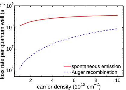
density we find a loss rate of 2.7×10⁸s−1 per quantum well which includes radiative as well as Auger recombina-tion, see Fig. 5. As the loss rate has to be compensated by the pumping, we demand
NQWRlossnthr= Ppump ¯
hωpumpα(ωpump) (1)
whereNQW is the number of quantum wells,Rlossis the carrier loss rate per quantum well,nthris the threshold
car-rier density,Ppumpis the pump power per pumped area, ¯
hωpump is the energy of the pump light, and α(ωpump)
carrier density (1012 cm−2)
loss rate per quantum well (s
−1
)
2 4 6 8 10
106 107 108 109
[image:7.612.62.271.93.243.2]spontaneous emission Auger recombination
Figure 5Laser losses due to spontaneous emission and Auger recombination as a function of the carrier density for an (Al0.108Ga0.785In0.107)As / (Al0.26Ga0.74)As quantum well at a temperature of 350 K.
In this manner, we estimate the threshold pump power as a function of the pump wavelength (Fig. 6). Obviously the efficiency of in-well pumping will drop rapidly if the pump wavelength is too close at the lasing wavelength. As soon as the pump wavelength exceeds a value of 822 nm, the required pump power increases drastically. In this spec-tral region the absorption is bleached out already by the induced generated carriers, thus limiting the pump wave-length.
The experimentally applied threshold pump intensity is 4.5×10⁸W m−2 for a pump wavelength between 806 nm and 810 nm. This corresponds quite well to the theoreti-cal estimation. Differences could be caused by the fact that only parts of the pumped area contribute to lasing, thus the experimental threshold pump power per area might be larger. Moreover, in the calculation we assume each quan-tum well to be excited with equal power, but the absorption of the pump radiation might be rather inhomogeneous due to the fact that the standing wave distribution of the pump does not equal that of the laser and hence its anti-nodes are not optimally overlapping with the quantum wells.
It is worth noting that it is essential for the analysis to have the microscopic model allowing for quantitative pre-dictions of the optical properties of the gain element in the VECSEL device. Simpler models would lead to incorrect conclusions as the lasing performance depends substan-tially on the spectral position of the quantum well absorp-tion/gain, its amplitude, the line shape of the spectra as well as the temperature and carrier density of all these quanti-ties. And besides, if the extracted threshold carrier density was incorrect, the error would be even further enhanced in the determination of the laser loss processes which react very sensitively to the assumed carrier density. The many-particle approach has proven to simulate all these aspects realistically, thus allowing for an accurate characterisation. Hence, in particular the potential and limitations of optical
drastic increase of the pump power required to reach threshold
pump wavelength (nm)
pump power (10
9 W m
−2
)
740 760 780 800 820 840
0 1 2 3
Figure 6Pump power needed to sustain the threshold gain as a function of the pump wavelength. For the evaluation a tempera-ture of 350 K is assumed in the active region.
in-well pumping for the 850 nm VECSEL could be anal-ysed with special emphasis on the bleaching of the pump absorption. One important consequence is that pump and lasing wavelength should be separated in this system by at least 25 nm to sustain the necessary threshold gain. This means, that 800-810 nm diodes can pump the 850 nm laser system quite efficiently.
It is interesting to investigate whether other material systems and wavelength regions can benefit from in-well pumping. For example, deep-blue and ultraviolet GaN diodes might be used to pump blue-green VECSELs and 670 nm diodes to drive VECSELs in the 700-750 nm re-gion. Obviously, a microscopic theory as developed here will be very helpful in assessing these situations.
4 (AlGaIn)(AsSb)-based lasers for long-wavelengths Semiconductor lasers emitting around 2μm are of considerable interest for a multitude of applications, such as medical diagnostics, material pro-cessing or spectroscopic trace gas detection. Based on the (AlGaIn)(AsSb) material class various designs with emission wavelength from 1.8μm up to 3μm have been presented, including diode lasers as well as VECSEL devices [30–35].
In order to study the basic optical properties of a pos-sible material system in the long-wavelength regime, we analyse the absorption/gain of a (GaIn)Sb quantum well structure emitting around 2μm by means of our micro-scopic approach. Here, we use our quantitative theory to deduce experimentally not directly obtainable quantities, in particular band-structure details. Besides the laser gain, also the laser loss processes are studied with the goal to explore the potential of different laser designs.
[image:7.612.314.522.99.243.2]type-II “W” active regions [36]. Again, the physical processes affecting the lasing parameters of such a device can be analysed by our microscopic approach.
4.1 Analysis of the laser gain properties For the wavelength regime around 2μm quantum well lasers em-ploying ternary (GaIn)Sb compounds are well suited. Based on the microscopic theory we analyse the material properties, in particular the optical gain, of such a (GaIn)Sb laser structure [12].
The GaSb-based diode laser we consider con-tains three 10 nm wide compressively strained (Ga0.78In0.22)Sb quantum wells which are sepa-rated by (Al0.30Ga0.70)(As0.02Sb0.98) barriers with a thickness of 20 nm. The active region is surrounded by 400 nm wide layers on each side, also made of (Al0.30Ga0.70)(As0.02Sb0.98). These, in turn, are embed-ded in (Al0.84Ga0.16)(As0.06Sb0.94) cladding layers. As the cladding layers have a considerably lower refractive index according to the higher aluminium concentration there is a remarkable jump of the refractive index from the barrier to the cladding layer on each side and thus, an optical waveguide is formed enclosing the laser mode in between. The overlap of the optical mode with the active layers, i.e. the three quantum wells of the system, determines a confinement factor for the laser structure of about 6.6 %. Actually, the amplification of the light mode through the system is given by the product of the confinement factor and the material gain provided by a single quantum well.
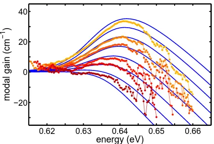
In order to study and analyse the gain properties of the laser structure, material gain spectra are computed based on the semiconductor Bloch equations for various carrier densities assuming a disorder-induced inhomoge-neous broadening of 10 meV. Multiplying these spectra with the confinement factor yields the modal gain of the laser structure (Fig. 7, solid lines). In this manner, the cal-culations can be compared to experimental spectra. Here, we use gain for a 500μm long and 6μm wide ridge waveg-uide laser at various excitation currents below threshold employing the method of Hakki and Paoli (Fig. 7, cir-cles). With growing excitation, the spectral width and am-plitude increase as well as the gain maximum becomes slightly blue-shifted. The spectral position of the gain peak matches within growth uncertainties and the line shape is also well reproduced.
The gain provided by the material system has a re-markably large amplitude exceeding that of more com-mon GaAs-based structures. For illustration, in Fig. 8 (top) material gain spectra of the (Ga0.78In0.22)Sb
quan-tum well are shown and compared to spectra obtained for the (Al0.115Ga0.785In0.10)As quantum well employed in the VECSEL addressed in Section 3. Since the calculation assumes the same temperature and equal carrier densities in both cases, one clearly observes that the gain amplitude is considerably higher in the (GaIn)Sb structure. The max-imal material gain which can be extracted is almost twice
energy (eV)
modal gain (cm
−1
)
0.62 0.63 0.64 0.65 0.66
[image:8.612.309.521.99.242.2]−20 0 20 40
Figure 7 Comparison of calculated (solid lines) and mea-sured (circles) modal gain spectra in the (Ga0.78In0.22)Sb / (Al0.30Ga0.70)(As0.02Sb0.98) laser structure at a temperature of 280 K for various excitations. In the simulation carrier densities of 0.65, 0.7, 0.75, 0.8, 0.85, 0.9, 0.95 and 1.0×1012cm−2(from bottom to top) are assumed. The spectra are shifted 4 meV to-ward higher energies which can be attributed to slight deviations of the actual growth from the nominal design. The experimental spectra are obtained employing the method of Hakki and Paoli for excitation currents of 12.7, 14.6, 16.9, 18.9, 20.8 and 22.8 mA (from bottom to top). The experiment was done by M. Rattunde, N. Schulz, and J. Wagner at the “Fraunhofer Institut f¨ur Ange-wandte Festk¨orperphysik”. [12]
the value obtained for the GaAs-based structure (Fig. 8, top, inset).
GaSb−based structure
GaAs−based structure
energy (eV)
material gain (cm
−1
)
0.6 0.7 0.8 1.3 1.4 1.5
0 1000 2000
carrier density (1012 cm−2)
gain maximum (cm
−1
)
0 5 10
0 1000 2000
in−plane wave vector (nm−1)
energy dispersion (eV)
ΔE = 0.644 eV ΔE = 1.488 eV
−0.5 0 0.5
−0.1 0 0 0.1 0.2 0.3
Figure 8 Top: Material gain spectra calculated for a
(Ga0.78In0.22)Sb / (Al0.30Ga0.70)(As0.02Sb0.98) quantum well (solid lines) and an (Al0.108Ga0.785In0.107)As / (Al0.26Ga0.74)As quantum well (dashed lines) at a temperature of 300 K. Car-rier densities of 1.0, 1.5, 2.0, 2.5 and 3.0 ×1012cm−2 (from bottom to top) are assumed. The inset depicts the maximum of the material gain as a function of the carrier density for both material systems. Bottom: Underlying band structure cal-culated for the (Ga0.78In0.22)Sb / (Al0.30Ga0.70)(As0.02Sb0.98) quantum well (solid lines) and the (Al0.108Ga0.785In0.107)As / (Al0.26Ga0.74)As quantum well (dashed lines). In order to com-pare the dispersion of the subbands in the two considered sys-tems, the effective band gapΔEis shifted to matching values in the figure.ΔEis 0.644 eV for the (Ga0.78In0.22)Sb and 1.488 eV for the (Al0.108Ga0.785In0.107)As quantum well.
4.2 Laser gain versus laser losses The high gain amplitudes provided by the (AlGaIn)(AsSb) material class are advantageous of course to construct a laser. However, one also has to keep in mind the laser loss processes. As the microscopic theory allows for quantitative predictions of both the gain and the losses, the tradeoff between them can be studied systematically in order to develop optimised designs for certain applications.
For illustration, we perform a detailed comparison of two different designs, each intended to have an emission wavelength of about 2μm at room temperature. While de-sign A is a 10 nm wide (Ga0.78In0.22)Sb quantum well
em-bedded in (Al0.30Ga0.70)Sb barriers, the quantum well of design B is 12 nm thick, has a slightly lower indium con-centration of 20 % and furthermore, the height of the bar-rier layers is reduced by employing (Al0.25Ga0.75)Sb.
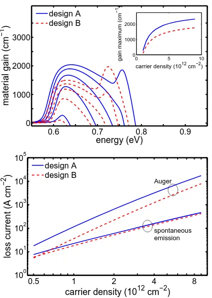
With these design specifications the material gain of both systems peaks at about 0.62 eV (Fig. 9, top). How-ever, the gain amplitude predicted for design A exceeds the amplitude expected for design B if equal carrier den-sities are assumed in the calculations. This aspect can be attributed to the fact that the carriers are less confined in design B due to the wider quantum well and the lower bar-rier height, thus the optical strength of the lasing transition is reduced. Maximally, a gain of about 2400 cm−1in case of design A and of about 1800 cm−1in case of design B can be extracted (Fig. 9, top, inset). These limits correspond to a saturation of the gain with increasing carrier density since a second peak grows out in the spectrum originating from higher order quantum well transitions.
In fact, the laser gain provided by design A is higher for a given carrier density, but the laser losses will be re-duced remarkable if design B is chosen. The results of the microscopically calculated loss current due to spontaneous emission and Auger recombination are given in Fig. 9 (bot-tom) for both designs in dependence of the carrier density present in the quantum well. The Auger losses are found to dominate the radiative losses in the entire carrier den-sity regime relevant for lasing, even at the transparency carrier density (about 0.9×1012cm−2 for design A and 1.0×1012cm−2for design B).
The radiative losses are slightly smaller for design B because the carriers are less confined in the quantum wells, thus reducing the probability of the spontaneous recombi-nation of an electron-hole pair. But what is rather crucial is that the Auger processes in design B are suppressed by more than a factor of two.
In order to assess the potential and limitations of the two proposed designs, we combine our quantitative knowl-edge about the laser gain and the laser loss properties. For this purpose, we extract the carrier density necessary to achieve a certain gain amplitude. Since this carrier density is connected to specific loss currents due to spontaneous emission and Auger recombination, we can evaluate the total loss current as a function of the material gain that is achieved (Fig. 10). To sustain the laser gain the total loss current has to be compensated by pumping the system, thus providing the appropriate number of carriers.
energy (eV)
material gain (cm
−1
)
0.6 0.7 0.8 0.9
0 1000 2000 3000
design A design B
carrier density (1012 cm−2)
gain maximum (cm
−1
)
0 5 10
0 1000 2000
spontaneous emission Auger
carrier density (1012 cm−2)
loss current (A cm
−2
)
0.5 1 2 4 8
100 101 102 103 104 105
[image:10.612.58.271.97.396.2]design A design B
Figure 9 Top: Material gain spectra calculated for a 10 nm wide (Ga0.78In0.22)Sb / (Al0.30Ga0.70)Sb quantum well, denoted as design A (solid lines) and a 12 nm wide (Ga0.80In0.20)Sb / (Al0.25Ga0.75)Sb quantum well, denoted as design B (dashed lines) at a temperature of 300 K. Carrier densities of 1, 2, 3, 4 and 5×1012cm−2(from bottom to top) are assumed. The inset depicts the maximum of the material gain as a function of the car-rier density for both material systems. Bottom: Laser loss current due to spontaneous emission and Auger recombination as a func-tion of the carrier density for design A (solid lines) and design B (dashed lines) at a temperature of 300 K.
a threshold gain peak of 500 cm−1, a threshold current of about 125 A cm−2has to be provided regarding design B. This amount is about 35 % smaller than the pump current which has to be applied to design A to achieve the same gain amplitude.
It is worth noting that Auger losses are particulary strong in materials with narrow band gaps. Considering the (GaIn)Sb quantum well, the Auger processes domi-nate the spontaneous recombination even at transparency and they increase drastically with growing carrier density (Fig. 9, bottom). In contrast, in Section 3 we investigate for instance a GaAs-based (Al0.115Ga0.785In0.10)As quantum well structure which has a band gap that is twice as large as the band gap of (GaIn)Sb, and for this system the con-tribution of Auger recombination plays a minor role com-pared to the radiative losses (Fig. 5). Because of the
par-material gain (cm−1)
total loss current (A cm
−2
)
100 200 400 800
102 103
design A design B
Figure 10Laser loss current including radiative and Auger re-combination as a function of the material gain provided for de-sign A (solid line) and dede-sign B (dashed line) at a temperature of 300 K.
ticular high Auger losses in the GaSb-based material sys-tem adequate designs are required to overcome these limi-tations. The comparison of design A and design B demon-strates that the potential of various structural layouts can be studied systematically on the basis of the microscopic approach. In this manner, structures with e.g. low thresh-old or high output power are found, so that laser devices can be optimised with regard to applications.
4.3 Investigation of mid-infrared type-II “W“ diode lasers The quantum-well structures presented in Section 4.1 and Section 4.2 are suitable for laser emission at 2.Xμm. However, if one aims for even longer emission wavelengths in the mid-infrared, their operation will be strong affected by high internal losses. To circumvent these limitations alternative concepts have been considered, in particular diode lasers with type-II “W” active regions are discussed [36]. They fill the spectral range between 3μm and 4μm given by type-I quantum well lasers on the short-wavelength side and by quantum cascade lasers [37] on the long-wavelength side. Based on the microscopic the-ory, we investigate the lasing properties of an antimonide type-II “W” diode laser structure emitting at 3.4μm [38].
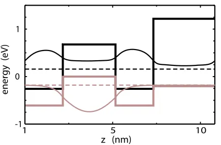
The laser structure consists of five so-called “W” elements [39]. Each is formed by a 3 nm wide (Ga0.925In0.075)Sb hole quantum well which is
[image:10.612.310.522.100.244.2]z (nm) -1
0 1
energy (eV)
[image:11.612.56.273.87.229.2]1 5 10
Figure 11Confinement potential for electrons (black, thick line) and heavy holes (gray, thick line) in the “W” element of the laser structure, which is formed by a layer sequence of InAs / (Ga0.925In0.075)Sb / InAs / (Al0.53Ga0.47)Sb. The thinly plotted curves indicate the lowest electron and the lowest hole confine-ment wave function respectively. The corresponding energy lev-els are marked as dashed lines.
By evaluating the laser gain and the laser losses mi-croscopically, we predict the threshold current of the laser diode in a temperature range between 80 K and 300 K. The results are in quantitative agreement with the exper-iment and a considerable increase of the threshold current with growing temperature is observed [38]. Through the microscopic analysis this behaviour can be attributed to a thermally reduced gain amplitude which involves higher threshold carrier densities and thus higher loss currents. In contrast, the Auger coefficient is found to be nearly tem-perature independent.
5 (GaIn)(NAs)-based material system After first reports of an increasing redshift of the band-edge lumi-nescence with increasing nitrogen content in 1992 [40], (GaIn)(NAs) has been under intense investigation for its potential application as a GaAs-based laser material at telecommunication wavelengths. The most widely known specialty of (GaIn)(NAs) and related materials is the huge, composition-dependent bandgap bowing which also ac-counts for the unexpectedly small bandgap. The intri-cate band structure may be described by the anticrossing model [41–43] where the nitrogen atoms are identified with an impurity band interfering with the conduction band. The resulting anticrossing pushes the conduction band edge to lower energies. In the formalism of k·p-theory, the
anti-crossing model corresponds to an extension of the 8×8 to a 10×10 k·p-matrix.
5.1 Characterisation of (GaIn)(NAs) structures
In order to use (GaIn)(NAs) material to its maximum po-tential, it has to be characterised thoroughly. However, be-ing a long wavelength material grown on GaAs, a number of characterisation measurements are hampered by sub-strate absorption. Photomodulated reflectance [44–46] of-fers a possibility to sensitively measure optical spectra
1.15 1.2 1.25 1.3 1.35
−20 −10 0 10 20
energy (eV)
PR & absorption (arb. u.)
absorption PR
PR
theory
exp
Figure 12Calculated (solid line) and measured (dotted line) pho-tomodulated reflectance spectra at a temperature of 300 K for a structure consisting of 9.4 nm wide (In0.23Ga0.77)As quantum wells between 35 nm wide Ga(N0.0048As0.9952) barriers. The cal-culated absorption spectrum (dashed line) is vertically displaced for clarity. Taken from [47].
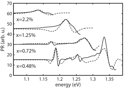
without substrate interference. This enabled a study of the type-I-type-II transition in a series of InGaAs-GaNxAs1−x samples. Four samples with nitrogen contents x=0.48%, 0.72%, 1.25%, and 2.2% were investigated [47].
Photomodulated reflectance experiments are per-formed by varying a modulation pump between zero and a small value while measuring the change in reflectance with the help of a probe beam. The microscopic simulation of photomodulated reflectance is not straightforward because the mechanism causing the reflectance change is largely unknown. Our calculations were performed by determin-ing the difference between two spectra at slightly varydetermin-ing densities. It is widely assumed that the modulation signal is caused by a change in electric field in the sample due to local charge inhomogeneities. We model these effects by solving Poisson’s equation but find the signals dominated by the pump-induced density change rather than the elec-tric field.
Figure 12 shows a calculated absorption spec-trum (dashed line) for a series of three 9.4 nm wide (In0.23Ga0.77)As wells between 35 nm wide Ga(N0.0048As0.9952) barriers and the corresponding
calculated photomodulated reflectance signal (solid line). For comparison, the experimental curve is also shown. Looking at the two theory curves for absorption and photo-modulated reflectance, we remark that the peak absorption energies are approximately given by the zero crossings of the differential signal. The calculation reproduces the main features of the experiment even without any line fitting parameters. The only adjustable quantity is the disorder-induced inhomogeneous broadening which was set to 6.7 meV to model the experiment.
[image:11.612.311.517.92.227.2]1.1 1.15 1.2 1.25 1.3 1.35 0
10 20 30 40 50 60 70
energy (eV)
PR (arb. u.)
[image:12.612.62.270.92.238.2]x=0.48% x=0.72% x=1.25% x=2.2%
Figure 13Calculated (solid lines) and measured (dashed lines) photomodulated reflectance spectra for the four samples inves-tigated here. The nitrogen content in the barriers varies from x=0.48%, 0.72%, 1.25%, to 2.2%. A type-I-type-II-transition can be shown to occur betweenx=0.72% andx=1.25%. The spectra are vertically displaced for clarity. Taken from [47].
less pronounced in the experiment, probably due to sample inhomogeneities. Regarding the lowest transition, we see it move to lower energies and lose oscillator strength from
x=0.48% to x=0.72% and attribute this effect to the de-creasing electron confinement. For thex=1.25%-structure the transition has vanished as a result of the type-I-type-II-transition with rising nitrogen content. In Ref. [47], this transition was further illustrated using a combination of ex-perimental methods.
These spectra are an example of a wide range of exper-iments in (GaIn)(NAs) which can be modelled by micro-scopic theory. Further works in this area may be found in Ref. [8, 48, 49].
5.2 Towards 1.55µm In recent years, the growth of high quality (GaIn)(NAs) material emitting at a wave-length of 1.55μm has increasingly become attainable. Even though progress has been slow due to the high in-dium and nitrogen contents involved, relatively low thresh-old lasers beyond 1.55μm have been demonstrated [50]. A major improvement in growth outcome may be achieved by the addition of antimony [51–55].
Our microscopic model allows us to consider the gain and loss properties of (GaIn)(NAs) in the entire 1.3– 1.55μm range independent of any growth issues [56], ad-dressing the question whether the degrading of optical properties at higher wavelengths is an intrinsic or a ma-terial quality related phenomenon. Figure 14 shows the intensity gain at 1.3μm (solid lines) and 1.55μm (dotted lines) in a quantum well structure containing 40 % indium. The nitrogen content was varied from 0.55% to 2.3% in order to change the emission wavelength.
(GaIn)(NAs) being a quaternary material, different compositions may be used to achieve emission at a specific wavelength. Samples with different indium and nitrogen contents but emitting at the same wavelength are also
0 1 2 3 4 5 6
0.7 0.8 0.9 1 1.1
1.8 1.6 1.4 1.2 1.1
material gain (103 cm-1)
[image:12.612.305.507.93.248.2]energy (eV) wavelength (μm)
Figure 14Intensity gain at 1.3μm (solid lines) and 1.55μm (dot-ted lines) for a quantum well structure containing 40 % indium. The dashed and dash-dotted lines show the effect of different strain which may be achieved by varying both indium and nitro-gen content, but keeping the emission wavelength constant. The dashed line corresponds to an unstrained sample. Obviously, the gain is much broader, and correspondingly the required carrier density is almost twice as high.
pared in Fig. 14. The dashed and dash-dotted lines show the effect of different compositions at a constant emis-sion wavelength of 1.3μm. For instance, the dashed line corresponds to an unstrained sample. Obviously, the gain is much broader, and correspondingly the required carrier density is almost twice as high as for the 40% indium struc-ture. To illustrate this dependence, we investigate two se-ries of materials:
A Constant indium: The indium content is kept at 40%, the wavelength is varied by changing the nitrogen con-tent.
B Constant strain: The strain is kept constant by varying both indium and nitrogen content.
Figure 15 shows the carrier density necessary to obtain a certain peak gain for the two material series at 1.3μm and 1.55μm. As discussed before, the density is lower for the highly strained samples with 40% indium content (exx =-2.65% for 1.3μm,exx=-2.35% for 1.55μm). This is also visible in the inset which is a magnification of the large figure for small gains.
Having access to the full information in our micro-scopic calculation, we can explain the effects in detail. The differences in required density are due to the band structure where composition changes induce the following effects:
1.Increased energetic separation of nitrogen level and conduction band edge for increased nitrogen content 2.Decreased electron mass for reduced nitrogen content
and increased indium content
0 5 10 15
0 1 2 3 4 5
carrier density (1012 cm-2)
gain maximum (103 cm-1)
40%In 1.55µm
40%In 1.3µm exx=-1%
1.3µm
exx=-1% 1.55µm
1 1.5
2
[image:13.612.60.253.85.222.2]0 0.5 1
Figure 15Carrier density necessary to obtain a certain peak gain for the two material series at 1.3μm and 1.55μm. Thick lines: Se-ries A, 1.55μm (dotted) and 1.3μm structure (solid). Thin lines: Series B, 1.55μm (dash-dotted) and 1.3μm structure (dashed). The inset is a magnification of the large figure for small gains.
gain (103 cm-1)
loss curr
e
nt / gain (
A
cm-1)
0 1 2 3 4
[image:13.612.313.524.304.597.2]0.3 1 10
Figure 16 Ratio of total loss current to peak gain. For the monomolecular loss, a monomolecular recombination time of 1 ns is assumed.
Comparing series A and B in the light of the above bandstructure dependencies, we remark that effect (2) and (3) lead to the observed higher gain for a given density for series A, while effect (1) weakens this phenomenon. In this quaternary material, one must thus strive to include as much strain as possible while still maintaining a high material quality.
Next, we microscopically calculate losses by Auger and spontaneous emission processes. Being a long wave-length material, Auger processes clearly dominate [56]. In order to identify the gain region where the excitation of the quantum well is most efficiently turned into light amplification, we divide the total loss current Jtot = Jmono +Jsp +Jaug by the peak gain. Here,Jmono,Jsp
andJaugare loss currents by monomolecular, spontaneous and Auger recombination, respectively. The monomolecu-lar contribution is caused by non-radiative recombination processes at defect states and thus, basically depends on the quality of the material. The corresponding loss current
is given byJmono = eτ−1ρ, where eis the unit charge,
τ= 1ns is a typical decay time in a (GaIn)(NAs) laser for 1300 nm emission [57], andρis the carrier density. The loss/current ratios show a clear minimum between 1000 and 2000 cm−1which is thus the optimum operation range for a laser.
In multi-quantum-well structures a reduction of losses can be achieved if the total number of quantum wells is adjusted such that the individual quantum wells operate in the optimum range. Pumping the quantum wells too hard, i.e. outside this regime, causes strong and dominant Auger losses. By contrast, close to the transparency point of the quantum well there are considerable monomolecular losses compared to a small gain.
5.3 Disorder in (GaIn)(NAs) So far, we included dis-order effects only phenomenologically via inhomogeneous
T=0.0K T=110K
Stokes shift (meV)
normalised PL
−1200 −100 −80 −60 −40 −20 0
1 2 3 4 5 6 7
temperature (K)
Stokes shift (meV)
0 50 100 150
−65 −60 −55 −50 −45 −40
[image:13.612.55.256.312.449.2]broadening. Even though this approach is appropriate for relatively homogeneous materials other systems, espe-cially quaternaries may suffer from more serious disorder effects due to alloying and interfaces. For a thorough theo-retical treatment of disorder, different regimes must be dis-tinguished. At room temperature and especially in the high density case discussed in Section 5.2, many-body effects rather than disorder dominate the signal. The opposite limit is the low temperature, low density regime where experi-mentally, strong disorder signatures are observed [58–62], in particular the so-called S-shape behaviour of the photo-luminescence energy and thus the Stokes shift. The effect consists of a non-monotoneous temperature-dependency, showing first a redshift, then a blueshift with rising tem-perature. The phenomenon is well-known in other materi-als [63, 64] and can be modelled in the framework of hop-ping of bound excitons in a tail of localised states inherent to (GaIn)(NAs) [62, 65] by employing the kinetic Monte Carlo algorithm suggested in Ref. [66]. A simulation of excitons hopping in a manifold of localised states with the exponential energy distribution
g(0) = N0 0 exp
0
(2)
is performed. Here,N0 is the concentration of localised states. For the energy scale 0 of the band tail in (GaIn)(NAs), a typical value of 10 meV is used [62, 65]. The phonon-assisted exciton hopping rateΓij from state
ito statejis determined by the Miller-Abrahams expres-sion [67]
Γij =ν0exp
−2rij
α −
j−i+|j−i|
2kT
(3)
whereν0is the attempt-to-escape frequency, which is usu-ally of the order of 1013s−1,rijis the distance between the localised sitesiandjwith energiesiandj, respectively,
αis the localisation length,kis Boltzmann’s constant and
T is the temperature. We use the following parameters in our calculation:N0α2= 0.6andτ0ν0= 2.0×10⁴
corre-sponding to the exciton lifetime ofτ0= 2.0ns.
Figure 17 (top) shows the calculated photolumines-cence spectrum assuming the exponential density of states given by Eq. 2. For low temperatures, excitons hop to their adjacent local minimum before recombining. With rising temperature, they become more mobile and are enabled to find deeper states within a wider distance to their origi-nal location, thus redshifting the luminescence. Fiorigi-nally, for temperatures on the order of0/k, the photoluminescence
spectrum increasingly mirrors the density of states [66]. In Fig. 17 (bottom) we display the temperature-dependent Stokes shift. The typical S-shape is clearly observable. The observation of the same trends as in experiments [62, 65] indicates that the low-temperature photoluminescence in (GaIn)(NAs) is dominated by disorder effects.
6 Ga(AsSb)-based emitters at 1.3µm Ga(AsSb) compounds constitute an alternative to the dilute nitride (GaIn)(NAs) material system in the domain of GaAs-based emitters operating at 1.3μm. The material has already been used in vertical-cavity surface-emitting laser (VC-SEL) systems [68], however, to fully explore the possibili-ties and to optimise the structural designs, the material sys-tem needs to be characterised in detail.
For a long time the band alignment of Ga(AsSb) em-bedded in GaAs for antimony concentrations of about 35 %, which are required to achieve emission at 1.3μm,
e1−h1
e1−h2
e1−h3 e2−h1
e2−h2
e2−h3 e3−h1
e3−h2 e4−h1
energy (eV)
absorption (cm
−1
)
0.95 1.0 1.05 1.1 1.15 1.2
0 0 5000 10000
0 kV cm−1 15 kV cm−1 difference x 2
energy (eV)
electroabsorption
+60 meV type II
+40 meV type II
no offset
experiment
0.95 1.0 1.05 1.1 1.15 1.2
[image:14.612.311.523.249.546.2]0 0 0 0
has remained an unresolved question. In fact, it was con-troversially discussed whether the structure is either type-I, where electrons and holes are confined in the Ga(AsSb) layer, or type-II, where electrons and holes are spatially separated in adjacent layers [69, 70]. As our microscopic analysis allows for a detailed analysis of the optical spec-tra, the controversial discussion on the confinement poten-tial can finally be clarified.
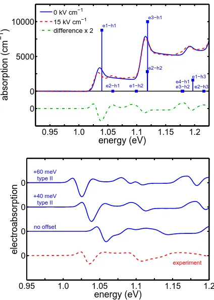
For this purpose we investigate a series of Ga(AsSb) / GaAs / (AlGa)As quantum-well structures by elec-troabsorption. The samples consist of a 7 nm wide Ga(As0.64Sb0.36) single quantum well with GaAs
spac-ers of varying width (0, 1, 2, 3, 6, 9 nm) on either side which are in turn placed within (Al0.25Ga0.75)As barrier layers [71]. In Section 5.1, we discuss the suitability of photomodulated reflectance investigations for the charac-terisation of quantum well structures; here we employ the electroabsorption method which is an adequate modulation technique as well. Experimentally, a square wave voltage is applied to the sample while the field-induced change in ab-sorption is measured [72]. In order to analyse and interpret the resulting spectra which are non-trivial in general, we calculate absorption spectra for two different electric fields applied in growth directions. Subtracting these two spectra from each other yields the electroabsorption signal. Due to the field-induced change of the oscillator strength, higher order quantum well transitions are also sensitively revealed (Fig. 18, top). Hence, the modulation technique is espe-cially useful for the characterisation of critical structural parameters.
The microscopic simulations demonstrate that the con-duction band offset between Ga(AsSb) and GaAs is the most sensitive parameter for the line shape. Through the comparison of calculated spectra for different offset situ-ations with experimental data we can conclude a spatially indirect confinement potential with a conduction band off-set of 40±20 meV (Fig. 18, bottom). In that case, the line shapes of both the first and the second resonance (around 1.04 eV and 1.12 eV respectively) are quite well repro-duced, and their spectral distance matches the experiment. The conclusion is verified by the investigation of electroab-sorption spectra for different external electric fields and for further samples [73, 74].
7 Nonequilibrium effects The characterisation of active materials and in particular the VECSEL properties presented in the previous sections result from a station-ary laser description with a quasi-equilibrium gain medium approach. However, the assumption of quasi-equilibrium carrier distributions disregards the effects of spectral hole burning and, in the case of optically in-well pumped de-vices, the bleaching of the absorption due to pump-induced blocking. Additionally, the effect of an enhanced carrier temperature compared to the lattice system is often ne-glected. Both, the nonequilibrium carrier distribution and the elevated carrier temperature, cause higher latent carrier
density and thus reduce the laser efficiency. Moreover, the active mirror heats up too, causing the so-called thermal rollover [5, 75–77].
To address nonequilibrium aspects, we could use the full semiconductor Bloch equations. However, since this requires excessive numerical calculations, we often resort to a systematically simplified approach. To separate the im-pact of the nonequilibrium carrier distributions from the heating effects of the mirror, we assume optimal heat con-ductivity to the external heatsink. Thus, the lattice tempera-ture of the active material is kept constant. Dynamical tem-perature changes involve additional solutions of the heat-conduction equations, which are numerically feasible but excluded here for simplicity.
As already introduced and used in the previous sec-tions, the description of the dynamic response of the laser device is performed in terms of equations of motion for the quantum well polarisation. However, in order to monitor the correct carrier distributions resulting from the contin-uous generation and recombination of carriers in the laser, additional microscopic equations of motion for the carri-ers have to be solved selfconsistently with the polarisation equations. The higher order Coulomb correlations occur-ring in the equations can be treated microscopically yield-ing the precise dynamics of carrier creation and scatter-ing [8]. This scatterscatter-ing is of an elementary nature for the description of the nonequlibrium carrier dynamics since the pump energy has to be higher than the laser energy. Thus, carriers injected with high pump energy¯hωpumpin the band have to scatter down to the band minimum where they can recombine stimulatingly.
The drawback of the rigorous scattering treatment [8] is the needed numerical effort resulting in very long calcu-lation times for the accurate laser dynamics. As a short-cut, we developed a scattering rate approach [78] with structural, temperature, density, and pump-energy depen-dent scattering rates. We use this method in combination with a dephasing time approach for the polarisation, yield-ing sufficiently fast numerics for the laser simulation. We have to underline at this point, that the predictivity of this model crucially relies on the correct scattering and dephas-ing times, which therefore have to be calculated separately with the full microscopic theory. The carrier losses due to spontaneous emission and Auger processes are calcu-lated via the microscopic theory already introduced in Sec-tion 2. Hence, the scattering-rate model preserves the mi-croscopic nature of our approach but sacrifices the full self-consistency in order to allow for significant reductions in computation time.
The model system under investigation is an (InGa)As-based VECSEL with a design wavelength of λlaser =1045 nm. We assume an active region con-sisting of 14 (In0.21Ga0.79)As quantum wells with 8 nm
Figure 19Quantum well absorption spectra calculated with the semiconductor Bloch equations for different equilibrium carrier distributions and a carrier temperature of 305 K. The plotted den-sities are (from gray to black):5×1011cm−2,1×1012cm−2,
2×1012cm−2,3×1012cm−2, and4×1012cm−2. The shaded area indicates the linear absorption of the quantum well.
An (AlGa)As cap layer finishes the active mirror which is then arranged with the external outcoupling mirror in a linear resonator geometry. For the calculations, an external mirror reflectivity of 98% is assumed.
The computed equilibrium absorption spectrum of the active material is shown in Fig. 19 for different carrier densities. Here, two conduction and five valence bands have to be taken into account to cover the spectral range from the quantum well band gap to the fundamental gap of the barrier, i.e. 1.55 eV. The shaded area in Fig. 19 is the linear absorption spectrum with clear excitonic signa-tures of the dipole transitions between the different bands under consideration. For higher densities, starting from
5×1011cm−2(dark gray) to4×1012cm−2(black), the
ex-citonic signatures wash out and reveal gain in the vicinity of the bandgap for sufficient large carrier density.
Our calculations show that carrier densities around
2×1012cm−2 are necessary for laser operation. Here, a
strong wavelength dependence of the quantum well ab-sorption is visible, especially a strong reduction of absorp-tion below 915 nm due to the Pauli blocking of the resident carriers (cf. Section 3.4).
The description of the laser is completed by a wave equation for the electrical field in the cavity. Together with the semiconductor Bloch equations, we get the Maxwell-Semiconductor Bloch Equations (MSBE), which allow for the modelling of the coupled electronic and optical features of the laser [79]. In the description of the pump field, we neglect the spectrally dependent reflection of the dielectric structure to directly monitor the impact of the nonequi-librium on the power characteristics. However, including these effects would just alter the pump-absorption effi-ciency to a product with this reflectivity (cf. the discussion of Section 3.4).
7.1 Optical in-well pumping In addition to the dis-cussion in Section 3, the strong wavelength dependence of
the quantum well absorption plays a crucial role for the choice of the optimal pump-wavelengthλpump for high power application. On the one hand side, a low pump-energy is desirable, due to the dependence of the internal conversion efficiency of the VECSEL on the quantum de-fectηQD = λpump/λlaser [7]. A high internal efficiency means low thermal losses and therefore less heat gener-ation leading to in principle higher possible output pow-ers. On the other hand, the absorption efficiencyηabsdrops with reduced pump energy as depicted in Fig. 19. Thus, the total efficiencyη =ηabsηQDηoutwith the outcoupling ef-ficiencyηout = lnR2/lnR1R2Tloss [7] of the device is reduced. Here,R1,R2 are the reflectivities of the Bragg
and external mirror, and1−Tloss the optical round trip transmission loss in the device. For high power applica-tions, this drawback of reduced pump absorption can be compensated by more complicated pump geometries, i.e. a recycling of the reflected pump light, see e.g. [22].
The calculated steady state VECSEL emission inten-sity of the quantum-well pumped device is shown in Fig. 20 (a) for incident pump intensities of 280 kW/cm2, 437 kW/cm2, and 984 kW/cm2. Here, the wavelength de-pendence of the absorption spectrum (Fig. 19) is resem-bled as anticipated: for a pump wavelength below 920 nm, the emitted intensity shows only a weak dependence on the actual pump wavelength. Above 920 nm, the pump ab-sorption drops due to the phase space filling. Hence, the creation of carriers due to the pump and thus the emission is reduced.
Corresponding to the emission intensity, the carrier temperatures and the steady-state carrier density show a strong wavelength dependence, as shown in Fig. 20 (b). The carrier temperatures are defined as the temperatures of the Fermi-Dirac distributions of the scattering rate ap-proach and thus are a measure of the mean energy of the particles in the corresponding bands. As depicted in Fig. 20 (b), the carrier temperatures of electrons and holes deviate from each other. This is a consequence of the par-ticular bandstructure. The plasma temperature Tplasma, plotted as the solid black line in Fig. 20 (b), is the mean temperature of all carriers in the quantum well. As al-ready stated before,Tplasma exceeds the lattice tempera-ture, which we set to 305 K, for all pump intensities. The increased carrier temperature is strongly influenced by the quantum defect which provides the largest fraction of the total dissipated heat. Consequently, the temperatures ba-sically follow the laser emission of Fig. 20 (a), leading to smeared out Fermi-Dirac distributions. This anticipates that the observed increase of the carrier density Fig. 20 (b, gray line) is a consequence of the carrier temperatures.
![Figure 17 Top:tom:nomenon may be observed experimentally in (GaIn)(NAs) [58–62] and serves as an indicator of exciton hopping behaviour](https://thumb-us.123doks.com/thumbv2/123dok_us/1690719.122443/13.612.60.253.85.222/figure-nomenon-observed-experimentally-indicator-exciton-hopping-behaviour.webp)