Rochester Institute of Technology
RIT Scholar Works
Theses Thesis/Dissertation Collections
8-1-2010
Cryptographic algorithm acceleration using
CUDA enabled GPUs in typical system
configurations
Maksim Bobrov
Follow this and additional works at:http://scholarworks.rit.edu/theses
This Thesis is brought to you for free and open access by the Thesis/Dissertation Collections at RIT Scholar Works. It has been accepted for inclusion in Theses by an authorized administrator of RIT Scholar Works. For more information, please [email protected].
Recommended Citation
Cryptographic Algorithm Acceleration Using CUDA Enabled
GPUs in Typical System Configurations
By
Maksim Bobrov
A Thesis Submitted in Partial Fulfillment of the Requirements for the Degree of Master of Science in Computer Engineering
Supervised by
Dr. Roy Melton
Department of Computer Engineering Kate Gleason College of Engineering
Rochester Institute of Technology Rochester, NY
August, 2010
Approved By:
_______________________________________________________________________________
Dr. Roy Melton
Primary Advisor — Dept. of Computer Engineering
_______________________________________________________________________________
Dr. Marcin Lukowiak
Secondary Advisor — Dept. of Computer Engineering
_______________________________________________________________________________
Thesis Release Permission Form
Rochester Institute of Technology
Kate Gleason College of Engineering
Title: Cryptographic Algorithm Acceleration Using CUDA Enabled GPUs in
Typical System Configurations
I, MAKSIM BOBROV, HEREBY GRANT PERMISSION TO THE WALLACE MEMORIAL LIBRARY TO REPRODUCE MY THESIS IN WHOLE OR PART.
_________________________________ Maksim Bobrov
Acknowledgements
This research would not have been possible without the invaluable support and guidance
of my advisor, Dr. Roy Melton. Special thanks go to my committee members, Dr. Marcin
Lukowiak and Stanislaw P. Radziszowski. Additionally, I acknowledge the Rochester
Institute of Technology for providing all the resources necessary to complete this
research. Lastly, I would like to thank all those that helped and supported me in any
Abstract
The need to encrypt data is becoming more and more necessary. As the size of
datasets continues to grow, the speed of encryption must increase to keep up or it will
become a bottleneck. CUDA GPUs have been shown to offer performance improvements
versus conventional CPUs for some data-intensive problems. This thesis evaluates the
applicability of CUDA GPUs in accelerating the execution of cryptographic algorithms,
which are increasingly used for growing amounts of data and thus will require
significantly faster encryption and hashing throughput. Specifically, the CUDA
environment was used to implement and experiment with three distinct cryptographic
algorithms — AES, SHA-2, and Keccak — in order to show the applicability for various
cryptographic algorithm classes. They were implemented in a system that emulates the
conditions present in a real world environment, and the effects of offloading these tasks
from the CPU to the GPU were assessed.
Speedups up to 2.6x relative to the CPU were seen for single-kernel AES, but
SHA-2 and Keccak did not perform as well as on the GPU as on the CPU. Multi-kernel
AES saw speedups over single-kernel AES up to 1.4x, 1.65x, and 1.8x for two, three, and
four kernels, respectively. This translates to speedups between 3.6x and 4.7x over CPU
implementations of AES. Introducing a CPU load had a minimal effect on throughput
whereas a GPU load was seen to decrease throughput by as much as 4%. Overall, CUDA
GPUs appear to have potential for improving encryption throughputs if a parallelizable
Table of Contents
THESIS RELEASE PERMISSION FORM ... II ACKNOWLEDGEMENTS... III ABSTRACT ... IV TABLE OF CONTENTS ... V LIST OF FIGURES ... VII LIST OF TABLES ... IX
CHAPTER 1 INTRODUCTION ... 1
CHAPTER 2 MOTIVATION ... 3
CHAPTER 3 CUDA PROGRAMMING MODEL ... 6
CHAPTER 4 AES ... 13
4.1. ALGORITHM OVERVIEW ... 13
4.2. GPUDESIGN AND IMPLEMENTATION ... 15
4.2.1 Direct Design ... 18
4.2.2 Lookup table Design ... 20
4.2.3 Implementation ... 21
CHAPTER 5 SHA-2... 22
5.1. ALGORITHM OVERVIEW ... 22
5.2. GPUDESIGN AND IMPLEMENTATION ... 24
CHAPTER 6 KECCAK ... 26
6.1. ALGORITHM OVERVIEW ... 26
6.2. GPUDESIGN AND IMPLEMENTATION ... 28
CHAPTER 7 TEST METHODOLOGY ... 31
7.1. ALGORITHM GPUPERFORMANCE ... 31
7.2. TYPICAL SYSTEM LOADING EFFECTS ... 32
CHAPTER 8 RESULTS AND ANALYSIS ... 34
8.1. SINGLE KERNEL GPUPERFORMANCE ... 34
8.1.1 AES ... 34
8.1.2 SHA-2 ... 38
8.1.3 Keccak ... 39
8.2. MULTI-KERNEL GPUPERFORMANCE ... 40
CHAPTER 9 CONCLUSIONS ... 49
BIBLIOGRAPHY ... 51
APPENDIX A AES CODE ... 53
APPENDIX B SHA-2 CODE ... 58
APPENDIX C KECCAK CODE ... 60
List of Figures
Figure 1: NVIDIA GPU vs. Intel CPU Performance Comparison [5] ... 6
Figure 2: CUDA Thread Hierarchy [5] ... 7
Figure 3: CUDA Hardware Architecture [4] ... 8
Figure 4: CUDA Process Flow ... 9
Figure 5: AES Encryption Algorithm ... 13
Figure 6: AES State Array [11] ... 14
Figure 7: Parallel AES in CTR Mode Implementation ... 16
Figure 8: S-Box Sub_bytes Implementation ... 18
Figure 9: Column Byte Selection ... 20
Figure 10: SHA-2 Algorithm ... 23
Figure 11: Keccak State [20] ... 26
Figure 12: Sponge Construction [21] ... 27
Figure 13: GPU Load Application ... 33
Figure 14: AES-128 Threads/Block Comparison ... 35
Figure 15: AES-192 Threads/Block Comparison ... 35
Figure 16: AES-256 Threads/Block Comparison ... 35
Figure 17: AES-128 Performance ... 36
Figure 18: AES-192 Performance ... 36
Figure 19: AES-256 Performance ... 37
Figure 20: AES Speedups ... 37
Figure 21: SHA-256 Performance ... 38
Figure 22: SHA-512 Performance ... 39
Figure 23: Keccak-256 Performance ... 39
Figure 24: AES-256 Multi-Kernel Comparison ... 40
Figure 25: AES Offloading Effects... 42
Figure 26: SHA-2 Offloading Effects ... 42
Figure 27: Keccak Offloading Effects ... 43
Figure 28: AES-256 CPU Load Effects ... 44
Figure 29: SHA-512 CPU Load Effects ... 44
Figure 30: Keccak-512 CPU Load Effects ... 45
Figure 31: AES-256 GPU Load Effects on Total Time ... 46
Figure 32: SHA-512 GPU Load Effects on Total Time ... 46
Figure 33: Keccak-512 GPU Load Effects on Total Time ... 47
Figure 34: SHA-512 GPU Load Effects on GPU Time ... 47
Figure 38: Keccak-224 Performance ... 64
Figure 39: Keccak-384 Performance ... 64
Figure 40: Keccak-512 Performance ... 64
Figure 41: AES-128 Multi-Kernel Comparison ... 65
Figure 42: AES-192 Multi-Kernel Comparison ... 65
Figure 43: AES CPU Load Effects ... 65
Figure 44: SHA-2 CPU Load Effects ... 66
Figure 45: Keccak CPU Load Effects ... 66
Figure 46: SHA-2 GPU Load Effects on GPU Time ... 67
Figure 47: Keccak GPU Load Effects on GPU Time ... 67
Figure 48: AES GPU Load Effects on Total Time ... 68
Figure 49: SHA-2 GPU Load Effects on Total Time ... 68
List of Tables
Chapter 1
Introduction
Vast amounts of data are stored and transmitted around the world at any given
time. Some, if not most, of this data is private information which the owner may not want
viewed publicly. To ensure that this does not happen, encryption algorithms are used.
However, many of these algorithms were designed in the early age of computers when
datasets were significantly smaller than they are now. Datasets which are now considered
average may take long periods of time to encrypt or hash. It is in the interest of security
to improve the performance of these algorithms.
The advent of the Compute Unified Device Architecture (CUDA) from NVIDIA
and ATI's FireStream Technology has shifted Graphics Processing Units (GPUs) from
primarily graphics enabling devices to general purpose stream processing devices. These
devices are a cost effective alternative to traditional parallel processing machines with
comparable performance. For certain applications, this change ushers in a new era in
computing which allows any modern personal computer to take advantage of parallel
processing capabilities previously available only in specialized systems.
This thesis attempts to leverage the benefits provided by the parallel architecture
of CUDA GPUs in the field of cryptography. Three algorithms were selected for
investigation; AES, SHA-2, and Keccak. CUDA implementations of each algorithm were
designed and implemented. Where published results were available for GPU
implementations, the algorithms in this thesis exhibited comparable performance. Each
implementation was then evaluated with varying CPU and GPU loads ranging from
determine the effects of offloading encryption and hashing algorithms from a CPU to a
GPU.
AES, which has a high degree of parallelism, saw speedups as high as 2.6x for
data sizes greater than 1 MB. SHA-2 and Keccak, on the other hand, have minimal
parallelism and thus saw no speedup. Performing each encryption and hashing with a
base CPU led to degradations of throughput up to 22%. A GPU load was found to
decrease the throughput by as much as 36%. Although these slowdowns would be
common in a typical system, the throughput may still be significantly faster when
utilizing the GPU. Thus, it is believed that CUDA enabled GPUs could play a role as
encryption and hashing accelerators in typical future systems.
The chapters that follow document the motivation, work, results and conclusions
of this thesis. Chapter 2 has a detailed discussion of the encryption and hashing problem
and why it should be investigated. Chapter 3 discusses the CUDA architecture, and
Chapters 4 through 6 describe AES, SHA-2, and Keccak, respectively. The test
methodology is discussed in Chapter 7, and the results of those tests are presented in
Chapter 2
Motivation
Since their introduction, computers have permeated all facets of modern life and
are now used for storing and transmitting information that is often of great value. To
ensure this information is accessible only to those with the clearance to see it, encryption
and hashing techniques have been established. However, dataset sizes today are much
larger than they were a decade ago so it may take minutes, or even hours, to encrypt or
hash what may now be considered a moderate dataset. This timing poses a problem to
many users from a convenience perspective — users are often unwilling to wait or may
not have the time — and, more importantly, it introduces a period of time during which
the data are vulnerable, which should be reduced as much as possible.
One solution to this problem is to reduce the dataset size. However, in many cases
the user does not have control (e.g., files produced by third party application). In cases
where the user does have some control, it may be difficult to produce any significant
reduction in size or may be undesirable to alter the data. Consequently, this solution is
not viable for many cases.
Alternatively, the implementation of the encryption or hashing algorithm can be
altered to execute faster. The case for parallelizing hash functions is made by Kaminsky
and Radsiszowski in [1]. They argue in favor of designing the next generation of hash
functions with a focus on potential for high throughput by way of parallelization. This
focus is necessary for hashing large datasets in reasonable amounts of time as well as
quickly hashing small datasets in specific applications such as on-the-fly hash message
authentication. A similar argument can be made for ciphers, although many already
Parallel implementations of encryption and hashing algorithms have seen success
on various platforms including ASICs and FPGAs. FPGA implementations of AES are
now capable of encryption throughputs as high as 9.22 GB/sec, more than 40 times faster
than the average CPU based implementation [2]. ASIC implementations have produced
speeds as high as 1.45 GB/sec, more than 6 times faster than the average CPU based
implementation [3].
In contrast, CPU implementations have lagged behind as a direct result of their
inherently serial nature. CPUs are best at performing sequential operations and are thus
limited in their ability to take advantage of any parallelism. Multi-core CPUs have
improved the CPUs ability to handle multiple threads of execution in parallel but are still
restricted to small numbers of threads. Consequently, typical computer systems have
traditionally relied on expensive expansion cards for high-speed encryption and hashing.
However, now all computers are equipped with some sort of GPU. The parallel
processing limitations inherent in CPUs can now be compensated by utilizing a GPU
capable of general purpose stream processing [4] [5]. Currently, two such GPU
technologies exist — NVIDIA’s CUDA [6] and ATI’s Stream [7]. Of these two, CUDA
is somewhat more developed and has had wider industry use [6] [7]. Thus, it has been
selected as the target platform for this thesis.
The algorithms selected for investigation were AES, SHA-2, and Keccak. These
were selected as they represent ciphers, the current generation of hash functions, and the
future generation of hash functions. Additionally, they fall into three classes of
chapters 4–6. The next chapter describes that NVIDIA CUDA platform targeted by this
Chapter 3
CUDA Programming Model
CUDA, developed by NVIDIA, is a highly parallel computing architecture
implemented on newer models of NVIDIA GPUs [6]. Unlike traditional GPUs, CUDA
GPUs are designed with greater focus on data processing as opposed to flow control and
caching. They are capable of executing thousands of lightweight threads simultaneously
with millions more queued. This high degree of parallelism leads to an immense increase
in potential performance such that current generation GPUs can vastly outperform
contemporary CPUs in certain applications. This comparison is visible in Figure 1.
However, these benefits cannot be realized by all applications. CUDA is based on the
stream processing model, which is an extension of the SIMD (single instruction, multiple
data) paradigm. This design paradigm, as the name suggests, makes CUDA optimal for
performing a single instruction many times, in parallel, on different sets of data. To better
understand how the SIMD paradigm is a key aspect of CUDA, an investigation of the
The CUDA architecture consists of two main components — the memory and the
processing cores — which work in conjunction and must be carefully considered when
designing an application. Memory is divided into five categories — global, constant,
textured, shared, and local — all of which have distinct features and can be accessed only
by certain groups of threads. Processor cores are divided into a hierarchy of blocks of
threads, and grids of blocks of threads. The thread hierarchy can be seen in Figure 2, and
[image:17.612.153.462.263.662.2]the overall architecture is shown in Figure 3.
Figure 3: CUDA Hardware Architecture [4]
The most basic unit of execution in the CUDA architecture is the thread. Each
thread is allocated a segment of local memory for local variables. Threads are grouped
into 1-dimensional, 2-dimensional or 3-dimensional blocks (up to 512 threads per block),
depending on application design. Each block has a unique section of shared memory
allotted to it which can be accessed by all threads belonging to that block. The block is
also the basic unit in terms of synchronization; all blocks execute independently, but
within a block, all threads are executed simultaneously and can be synchronized using the
synchthreads command. Finally, blocks are grouped into 1-dimensional or 2-dimensional
grids. All grids have access to global memory, which includes constant memory and
textured memory.
To facilitate software design, CUDA implements numerous extensions to the
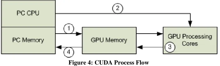
that is to execute on the GPU is called the kernel. Communication between the CPU and
GPU is achieved through memory reads and writes. Before executing a kernel, the data
that are to be processed must be transferred to memory on the GPU. Next, the CPU
initiates kernel execution on the GPU. Once execution is complete, the CPU retrieves the
processed data from the GPU. This process is illustrated in Figure 4. Since
communication between a CPU and its peripherals is relatively slow, the process of
copying data back and forth can often be a major bottleneck. Therefore, an important
aspect of an efficient CUDA implementation is the ability to overlap GPU
[image:19.612.132.484.321.427.2]communication from/to the CPU or from/to PC memory with GPU computation.
Figure 4: CUDA Process Flow
The performance enhancements obtainable with CUDA are heavily algorithm
dependent but there are some general guidelines which can be followed. The overall goal
is to maximize occupancy of the GPU such that each multiprocessor has the maximum
possible number of threads queued at any time. There are two main factors which
determine occupancy: register requirements per thread and shared memory usage.
As a thread executes, registers are allocated for that thread in order to store any
variables that are not explicitly stored in memory. However, the quantity of this storage is
limited per processor, and thus the number of registers available per thread is limited. For
example, the GTX 285 contains 16 KB of registers per processor and can execute a
a full occupancy of 1024 threads, each thread cannot use more than 16 registers. If the
register utilization per thread were increased beyond 16, the number of threads executing
would generally decrease. In the worst case scenario, some register values may be placed
in local memory. This is extremely detrimental to throughput as local memory is actually
a specially allocated portion of global memory, which is extremely slow.
If an application is found to utilize an excessive amount of registers or local
memory, it may be necessary to move some data to other types of memory. Shared
memory is the fastest memory available on the GPU and thus should be the primary
memory used. Its speed is a result of its proximity to the processing cores — it is the
CPU equivalent of cache but with complete user control. Additionally, all read and write
operations to shared memory are guaranteed never to miss. However, the quantity of this
memory is limited per processor. Since this memory is common to all blocks of a
processing core, excessive usage of this type of memory can limit the number of active
thread blocks per processing core. For example, the GTX 285 contains 16 KB of shared
memory per multiprocessor. Executing 256 threads per block with each block utilizing 4
KB of shared memory will produce occupancy of 100% as this configuration will allow
the maximum of 1024 threads to execute on each core. However, increasing the shared
memory usage per block to 8 KB will allow for only 50% occupancy since the number of
simultaneously active blocks is limited to two. If using a CUDA device with compute
capability 2.0 or higher, it may not be necessary or desirable to obtain full occupancy.
These devices are capable of executing multiple kernels simultaneously in parallel so it
If shared memory is not sufficient, global memory must be used. This type of
memory is significantly slower than shared memory but can be favorable if used
correctly. There are two subsets of global of memory — constant and textured. Unlike
global memory, constant, and textured memory are cached, greatly reducing the
probability of a miss and thus increasing throughput. Furthermore, each type of memory
is optimized for specific types of operations. Constant memory should be used when
many threads perform simultaneous reads from a single memory location. Textured
memory is preferred when memory accesses occur with either 1-D or 2-D spatial locality.
The final consideration when dealing with memory is how to maximize
coalescing. Coalescing is the combination of multiple small memory accesses into several
wide memory accesses. This combination takes place at the warp level. If the threads of a
warp perform a memory access which does not utilize the full width of the data bus, it is
possible that these memory accesses may be combined into a smaller set of larger
memory accesses. For example, the data bus on the GTX 285 is 64 bytes wide. If all 32
threads of a warp were each to perform a four-byte memory read, instead of performing
32 reads, these reads could be coalesced into two reads of 64 bytes to improve
performance by a factor of 16. This optimization occurs only when the threads of a warp
read memory in sequential order. An additional problem may arise if the memory access
is not correctly aligned with memory. A CUDA word is 64 bytes; however, memory is
partitioned into 128-byte blocks. If the memory access spans multiple words, both of
which do not fall in the same 128-byte block, two memory accesses are required for a
In addition to maximizing occupancy and properly utilizing memory, it is
important to minimize the amount of branching per thread. Branching refers to any
variations in execution paths amongst threads. Unlike a traditional CPU scheduler which
schedules a single thread at a time, the CUDA scheduler schedules threads in “warps” of
32 threads. For a warp to be considered done and a new one scheduled in its place, all
threads of that warp must finish executing. Thus, ideally all threads in a warp should take
an equal amount of time to execute so that no warp thread waits idly for other threads in
the warp to finish. This condition can be ensured by reducing or completely removing
branching.
Finally, it is important to decrease the number and size of data transfers between
the CPU and GPU as they are often the largest bottleneck when working with CUDA.
Data transfers occur over the PCI Express bus which has a bandwidth of 16 GB/sec for
the most recent generation (older generations are much slower at 4 GB/sec and 8
GB/sec). Meanwhile, the bandwidth of the memory on the 280GTX is approximately 130
GB/sec, more than eight times faster than the PCI Express bus. Thus, it is imperative that
data transfers are minimized as much as possible. Future generations of CUDA devices
may mitigate this issue by combining the CPU and GPU into a single device, which
would effectively remove the need for data transfers all together [9].
The next chapters describe the encryption and hashing algorithms. The design and
implementation of each algorithm with CUDA is discussed. Preliminary results used to
Chapter 4
AES
The Advanced Encryption Standard (AES) was first introduced in 1998 as the
Rijndael algorithm. In 2001, after a five-year standardization process, it was selected by
the National Institute of Standards and Technology (NIST) as the most suitable
replacement for its predecessor, the Data Encryption Standard (DES) [10]. Since then, it
has become one of the most popular encryption algorithms and is likely the most widely
used block cipher today. It has been selected as a candidate for this thesis as a direct
result of its popularity — improving the performance of this algorithm may be very
beneficial to its future users.
4.1. Algorithm Overview
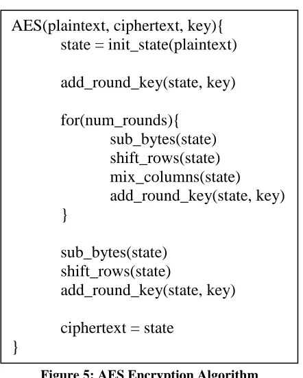
AES is based on the principles of substitution-permutation networks (SP
[image:23.612.197.418.373.649.2]networks); the process of encryption utilized by AES is roughly divided into two major
Figure 5: AES Encryption Algorithm
AES(plaintext, ciphertext, key){ state = init_state(plaintext)
add_round_key(state, key)
for(num_rounds){ sub_bytes(state) shift_rows(state) mix_columns(state) add_round_key(state, key) }
sub_bytes(state) shift_rows(state)
add_round_key(state, key)
functions: substitution and permutation [11]. These substitutions and permutations, along
with key based operations, are performed multiple times on the input data to obtain the
encrypted ciphertext. An overview of this algorithm is presented in Figure 5.
To begin, the plaintext to be encrypted is divided into 16-byte segments. As a
block cipher, AES operates on fixed-length blocks of data. These blocks are then
converted into a 4x4 array of bytes, known as the state, as illustrated in Figure 6. The
[image:24.612.105.511.263.384.2]shading signifies grouping of bytes in columns.
Figure 6: AES State Array [11]
The substitution portion of the cipher, referred to as sub_bytes in Figure 5, is a
simple replacement of each byte in the array with its entry in a fixed 8-bit substitution
box (s-box), as in the Rijndael s-box. This value can also be calculated mathematically.
The permutation portion of the cipher is split into two functions: shift_rows and
mix_columns in Figure 5. Shift_rows performs a row permutation in the form of a
left-circular shift on each of the four rows of the state starting with a zero shift for the top row
and increasing by one for each consecutive row. Next, mix_columns performs a column
permutation which can best be described as a matrix multiplication as shown in (1). C is
the pre mix_columns state and C’ is the post mix_columns state. Alternatively, both
4 4 4 4 3 4 4 4 4 2 1 4 4 4 3 4 4 4 2 1 4 4 4 4 3 4 4 4 4 2 1 C A C C C C C C C C C C C C C C C C C C C C C C C C C C C C C C C C C = ′ ′ ′ ′ ′ ′ ′ ′ ′ ′ ′ ′ ′ ′ ′ ′ ′ 33 32 31 30 23 22 21 20 13 12 11 10 03 02 01 00 33 32 31 30 23 22 21 20 13 12 11 10 03 02 01 00 02 01 01 03 03 02 01 01 01 03 02 01 01 01 03 02 (1)
Finally, the key is incorporated during add_round_key in Figure 5. At each round,
the round key is determined using Rijndael’s key schedule. It is then added to the state
via a bitwise XOR.
To increase the security of block ciphers like AES, numerous modes of operation
have been developed [12]. These modes modify the algorithm in order to ensure that
identical message blocks encrypted at different positions in the plaintext with identical
keys will not produce equal values. This thesis focuses on counter mode (CTR) which
performs the AES encryption on a counter value and XORs the result of that with the
corresponding message block to obtain the encrypted output. CTR mode presents two
beneficial qualities which can be advantageous in a CUDA implementation. First, it
preserves the block-level parallelism, which represents the bulk of the parallelism
available in AES. And second, its encryption of a counter value instead of the plaintext
provides the potential for reducing data transfers between the CPU and GPU; the final
XOR can be performed on either the GPU or CPU.
4.2. GPU Design and Implementation
Many instances of parallelism are inherent in the AES algorithm [13][14]. A
coarse-grained level of parallelism is provided by the independence of each 16-byte
block, allowing all bytes of a block to be encrypted independently of each other. This
considered in this thesis. Within each block encryption, each function within a round can
be performed independently of other instances of that function: an s-box substitution can
be performed on each byte independent of any other byte, each row can be shifted
independent of any other row, each column can be mixed independent of any other
column, and each word of the round key can be added independent of any other round
word. To achieve the desired maximum occupancy, it is necessary to consider only the
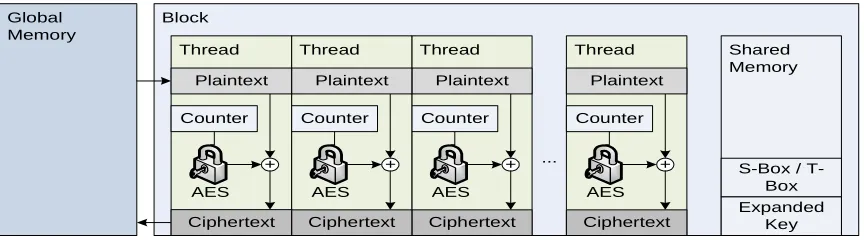
coarse grained parallelism provided by individual data blocks. Each CUDA thread
completes the AES encryption on a single 16-byte block of data. All 16-byte blocks are
computed in parallel. Implementing the aforementioned block level parallelism would be
[image:26.612.93.525.347.467.2]beneficial only for smaller datasets, which do not generate full occupancy of the GPU.
Figure 7: Parallel AES in CTR Mode Implementation
Two methods of implementing AES were investigated: a direct approach and one
using lookup tables (LUTs). Figure 7 illustrates the overall approach to both designs; the
two methods vary in the specifics of how they implement the AES step. All other steps
are common to both implementations. To begin, Rijndael’s key expansion algorithm is
used to compute the key schedule. This computation is performed on the CPU so that
each thread does not have to replicate this process as the key schedule is identical for
every block. The key schedule is then copied to the GPU along with the data and any
Block Thread Shared Memory Global Memory + Counter Ciphertext AES Plaintext
block is assigned a thread. The number of CUDA blocks is calculated based on the total
number of threads and the chosen threads per block value (the details of this choice are
further discussed in Chapter 8.1.1).
The kernel that is to perform the AES encryption is started with the calculated
number of threads and blocks. The first thing each thread does is determine its unique
identification number. This id number is used to determine the counter value required for
CTR mode and to access the proper portion of the dataset. Next, the threads of each block
collectively move all necessary LUTs from global memory to shared memory. Once the
threads have transferred all the necessary LUTs, they are synchronized, and the counter
value is encrypted.
The final step is to XOR the encryption of the counter with the corresponding data
block. This operation reads the data directly from global memory and writes the result
back to the same location in global memory. Shared memory is not used in this case since
it does not remove the need to read and write global memory once and actually adds the
need to read and write shared memory once. Once all threads have completed this process
the kernel returns, and the CPU transfers the encrypted data from GPU memory to CPU
memory.
It was found that a significant improvement in performance can be achieved by
moving the final XOR operation from the GPU to the CPU. This removes the need to
transfer the plaintext data from the CPU to the GPU effectively reducing data transfers by
50%. To obtain the full performance benefits, the kernel was divided into four
mini-kernels. This division allowed for the pipelining of kernel execution, data transmission
4.2.1 Direct Design
This design took a direct approach to implementing AES. Each function is
implemented individually as shown in Figure 5. Little effort is required to implement the
shift_rows function as it can be done as a bitwise circular shift or, as it is done in this
case, by simply remapping the registers. The add_round_key function is also very
straightforward requiring a single XOR per column. The sub_bytes and mix_columns,
however, required investigation of different design options.
Sub_bytes
The sub_bytes function can be implemented in one of two ways — using an s-box
lookup table or calculating the value. Both approaches were implemented and tested to
determine which would perform best.
The s-box approach requires the use of a lookup table, which requires multiple
memory reads. This approach can be optimized by moving the table to shared memory as
was done in this case. However, the use of lookup tables is discouraged as it increases the
susceptibility of the implementation to side channel attacks [15]. Figure 8 shows the code
to implement the s-box approach in CUDA C.
On the other hand, the calculation requires no memory lookups; it is done as a
serious of basic arithmetic operations. Traditionally, the calculation is done using the
extended Euclidian Algorithm to calculate the multiplicative inverse of a value and then
Figure 8: S-Box Sub_bytes Implementation
uint8_t __host__ __device__ subByte(uint8_t b, uint8_t *sbox){ return sbox[b];
in its use of the extended Euclidian Algorithm which is non-deterministic and will lead to
an increase in branching.
An alternative method is to use composite field arithmetic to convert values from
GF(28) to GF(((22)2)2) [16]. This is beneficial in two ways. First, operations in this field
are simpler — addition is equivalent to XOR, and multiplication is equivalent to AND.
Second, these computations are deterministic and, as such, will not result in branching.
Both techniques were tested, and the s-box approach was actually found to be
approximately ten times faster. Its better performance is likely because of the complexity
of the implementation chosen for the calculation method, which required dozens of XOR,
AND, and inverting operations. Alternative calculation implementations may exist which
would perform better. As a result, the s-box approach is used in the final design.
Mix_columns
The other function which needed investigation was mix_columns. Performing the
matrix multiplication would require a significant number of polynomial multiplications,
which are both slow and non-deterministic. However, it is possible to take advantage of
the simplicity of the polynomial multiplications required. Multiplying by 0x01 produces
the original value, multiplying by 0x02 can be implemented as a bitwise left shift of one
and an XOR with 0x1B if the most significant bit of the original value is a one [11], and
multiplying by 0x03 can be implemented as multiplying by 0x02 and an XOR with the
original value. Even with this improvement, mix_columns still remains the slowest part
of the encryption consuming approximately half the time of the full algorithm. It is also
4.2.2 Lookup table Design
This design condenses the functions of a round into four table looks ups and four
XORs per column. The four necessary tables, referred to as T-boxes, are constructed as
shown in (2). These tables are the results of performing the sub_bytes, and mix_columns
operations of a round on every possible 8-bit value.
⊕ = − − − j j j j C j C j C j j j j j j k k k k a S a S a S a S e e e e , 3 , 2 , 1 , 0 3 , 3 2 , 2 1 , 1 , 0 , 3 , 2 , 1 , 0 ] [ ] [ ] [ ] [ 02 01 01 03 03 02 01 01 01 03 02 01 01 01 03 02
[ ]
[
]
[
]
[
]
⊕ ⊕ ⊕ ⊕ = − − − j j j j C j C j C j j j j j j k k k k a S a S a S a S e e e e , 3 , 2 , 1 , 0 3 , 3 2 , 2 1 , 1 , 0 , 3 , 2 , 1 , 0 02 03 01 01 01 02 03 01 01 01 02 03 03 01 01 02 • • = • • = • • = • • = 02 ] [ 03 ] [ ] [ ] [ ] [ ] [ 02 ] [ 03 ] [ ] [ ] [ ] [ ] [ 02 ] [ 03 ] [ ] [ 03 ] [ ] [ ] [ 02 ] [ ][ 1 2 3
0 a S a S a S a S a T a S a S a S a S a T a S a S a S a S a T a S a S a S a S a T j C j C j C j j
j
T
a
T
a
T
a
T
a
k
e
=
0[
0,]
⊕
1[
1, − 1]
⊕
2[
2, − 2]
⊕
3[
3,− 3]
⊕
(2)A round consists of using the four bytes of a column as indices into the T-boxes.
The shift_rows operation is included in the selection of the bytes of each column as
illustrated in Figure 9. Every four bytes of a single pattern represent the four bytes of a
column. The results of these lookups are XORed along with the corresponding word of
These tables are constructed to function for the intermediate rounds, not the first
and last rounds. These two rounds are performed a single function at a time in the same
manner as the direct design and, in fact, use the optimized functions from that design.
To improve performance, the t-boxes, the s-box and the expanded key are moved
from global memory to shared memory. All other operations are performed in registers.
Similar to the s-box of the direct design, the t-boxes increase the susceptibility of
the implementation to side channel attacks [15]. However, they also provide potential for
significant speedups. Whether security or throughput is more important is left up to the
user.
4.2.3 Implementation
The direct design was found to outperform the LUT design by approximately 10%
and was consequently used as the final design for testing. Appendix A provides the code
for this implementation. Future modification to both implementations may change
performance. Possible points of investigation include alternate sub_bytes and
mix_columns implementations for the direct design. The LUT design could benefit from
varying the memory type used as well as alignment in memory.
In addition to ciphers, hashing algorithms are often used for encryption. The next
Chapter 5
SHA-2
In 1993, NIST introduced the first version of the Secure Hash Algorithm (SHA)
— SHA-0. Shortly thereafter, in 1995, SHA-0 was superseded by SHA-1 in order to
improve its security. In 2001, four additional hash functions (224, 256,
SHA-384, and SHA-512), collectively known as SHA-2, were added to improve security
further [10]. The SHA-2 family is currently considered one of the most secure hash
algorithms, which makes it a good candidate for performance analysis.
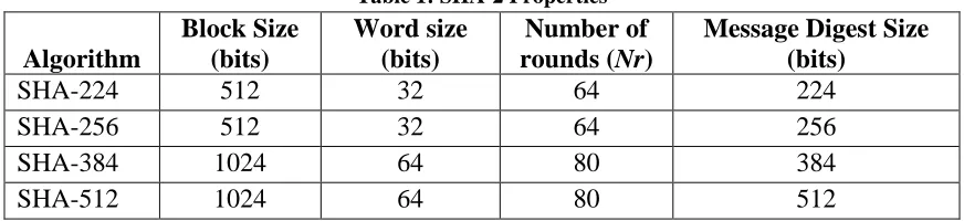
5.1. Algorithm Overview
The SHA-2 functions utilize a single underlying algorithm with varying block
sizes, word sizes, number of rounds (Nr), and message digest sizes [10][11]. These values
can be seen in Table 1. Additionally, SHA-224 and SHA-256 use different word rotation
[image:32.612.88.524.443.543.2]functions and constants than SHA-384 and SHA-512 due to their different word sizes.
Table 1: SHA-2 Properties
Algorithm
Block Size (bits)
Word size (bits)
Number of rounds (Nr)
Message Digest Size (bits)
SHA-224 512 32 64 224
SHA-256 512 32 64 256
SHA-384 1024 64 80 384
SHA-512 1024 64 80 512
The underlying algorithm consists of two stages: preprocessing and hash
Preprocessing prepares the message for hashing. First, the binary version of the
message is padded with a 1 followed by k 0s and n bits containing the binary
representation of the size, in bits, of the message. k is the number of bits required to make
the message a multiple of the block size, and n is double the word size. Finally, the
message is parsed into an array M of N blocks based on the block size of the chosen
function.
Once preprocessing is complete, the hash computation can begin. The message is
incorporated into the hash via the message schedule, W, which is calculated based on (3).
< ≤ + + + < ≤ = − − −
− W W W t number of rounds
[image:33.612.149.465.67.416.2]W t M W t t t t t t _ _ 16 ) ( ) ( 16 0 16 15 0 7 2 1 σ σ (3)
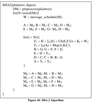
Figure 10: SHA-2 Algorithm
SHA2(plaintext, digest)
DM = preprocess(plaintext) for(N=sizeof(M)){
W = message_schedule(M);
A = M0; B = M1; C = M2; D = M3;
E = M4; F = M5; G= M6; H = M4;
for(t < Nr){
T1 = H + Σ1(E) + Ch(E,F,G) + Kt + Wt;
T2 = Σ0(A) + Maj(A,B,C);
H = G; G = F; F = E; E = D + T1;
D = C; C = B; B= A; A = T1 + T2;
}
M0 = A + M0; M1 = B + M1;
M2 = C + M2; M3 = D + M3;
M4 = E + M4; M5 = F + M5;
M6 = G + M6; M7 = H + M7;
Next, the working variables a, b, c, d, e, f, g, and h are set to the hash values H of
the previous block. In the case of the first round, the working variables are initialized to
constant values based on the chosen function. The round function, seen in (4), is then
executed Nr times.
2 1 1 0 2 1 1 ) , , ( ) ( ) , , ( ) ( T T A A B B C C D T D E E F F G G H C B A Maj A T W K G F E Ch A H
T t t
+ = = = = + = = = = + Σ = + + + Σ + = (4)
Once the round function is complete, the working variables are XORed with the
hash values of the previous round to produce the hash values for the current round. The
hash computation step is repeated for each block of the message. The digest is the final
result, H, of the last block processed.
5.2. GPU Design and Implementation
SHA-2 is a very serial algorithm and thus lacks any significant parallelism.
Therefore, SHA-2 is not a good candidate for parallel speedup from SIMD GPU
processing. Nevertheless, it may be beneficial to offload the hashing process from the
CPU to the GPU, which could produce an overall speedup from the heterogeneous
the algorithm is implemented serially. Thus, no optimization for the CUDA architecture
was performed. If multiple simultaneous hashes were desired, each independent hash
computation could be done in parallel with CUDA. If enough such parallel hashes were
performed, a benefit may be seen.
Although SHA-2 is still widely used, a competition is currently going on to find
its replacement, which will be known as SHA-3. The next chapter discusses Keccak, one
Chapter 6
Keccak
As part of an effort to advance beyond current security methods, the NIST
announced a competition in 2007 to find a successor to the current generation of hash
algorithms [17]. A total of 61 algorithms were suggested for the first round of the
competition. They were narrowed down to 14 in 2009. The final result of the competition
will be known at the end of 2012. The algorithm selected will most likely replace the
current generation of hashing algorithms. Thus, it is important to look at the performance
of this future class of algorithms.
For the purpose of this thesis, Keccak [18] was selected as the representative
SHA-3 algorithm. The SHA-3 candidates vary widely in their underlying structures,
which makes it difficult to select one that perfectly represents all the candidates. Keccak
was selected purely out of interest and the lack of published research into it. The only
study of Keccak currently available is into its susceptibility to cube attacks [19].
[image:36.612.211.403.489.687.2]Keccak is based on the sponge construction proposed by Bertoni, Daemen,
Peeters, and Assche in [18]. The sponge construction consists of two steps: absorbing and
squeezing. It operates on a state consisting of b=r+c bits where b is the state size, r
(known as bitrate) is the predetermined block size, and c (known as capacity) is used to
establish the security of the algorithm. The Keccak state is arranged in a 5x5 array of
64-bit lanes as show in Figure 11. In order to perform absorption and squeezing, the sponge
construction requires a function, f, which is used to interleave the data. f can be any
transformation or permutation but should be chosen carefully as security of the overall
sponge is highly influenced by the function selected. The absorption phase absorbs the
input message one r-bit block at a time. It incorporates each block into the state by
XORing it with the state and then scrambling the result using f. Absorption continues
until all blocks of the message have been absorbed at which point squeezing may begin.
Squeezing, like absorption, uses the function, f, to scramble the data further. The number
of squeezing steps is independent of all previous steps and can be varied based on desired
output size. The sponge construction process explained above is concisely represented in
Figure 12.
Since Keccak is based on the sponge construction, it follows the same procedure
of absorbing and squeezing utilizing a specific function f. The function selected is a
permutation block cipher similar to AES but with some security improvements based on
research done since the inception of AES [22][18]. The core of the function is
represented as a series of equations shown in (5). Rot refers to a left-shift of some number
of bits, R defines the shift value for each lane, and RC is a round constant. Seven
variations of this function exist based on the desired state size, b. Acceptable values are
b= 25 x 2l, where l is in the range 0 to 6. The complete function consists of 12+2l rounds
of (5).
θ:
ρ and π: x:
i:
, 0 Ax, 1 Ax, 2 Ax, 3 Ax, 4 1 rotCx 1, 1!
, " , " Dx $", 2 3" %&', ", (, "! , " $, " ~Bx 1, y Bx 2, y!
A0,0A0,0 RC
(5)
The final Keccak specification lists four versions of Keccak with varying bitrate
and capacity values. These are Keccak-224, Keccak-256, Keccak-384, and Keccak-512.
Their respective bitrate and capacity can be found in Table 2. The number associated
with each name corresponds to the output digest size in bits.
Table 2: Keccak Properties
State Size (b) Bitrate (r) Capacity (c) Output Length (o)
Keccak-224 1600 1152 448 224
Keccak-256 1600 1088 512 256
Keccak-384 1600 832 768 384
Keccak-512 1600 576 1024 512
function within a round can be done independent of the rest. Full occupancy is not
attainable with this limited parallelism, but a CUDA implementation should still be able
to produce speedups as high as 25x if all 25 lane calculations can be performed
simultaneously. This is the approach attempted by this thesis. The CUDA C
implementation can be seen in Appendix C.
Like with the previous algorithms, the data are first padded and then transferred to
the GPU along with the round constants (RC) and rotation constants (R). The kernel is
then launched with 25 threads arranged in a 5x5 grid to match the lane configuration of
the state. Each thread is associated with a lane in the state based on its (x, y) coordinate in
the 5x5 grid. Next, the round constants are moved to shared memory, with each thread
moving a single value. The state array is then declared as a 5x5 subset of 64-bit words in
shared memory, and each thread initializes its respective lane to 0.
Once setup is complete, the absorption process begins. This process is serial in
nature since each block of the input message must be absorbed and processed by the
function f in sequential order. However, each block consists of 25 64-bit words which can
be read in parallel. This parallelism is accomplished by having the first 25 threads read
the corresponding words into their respective lanes.
The function f is also serial in nature as it is a series of rounds applying the round
function found in (5). However, the bulk of the parallelism found in Keccak is located
within the round function. Initially, Keccak was implemented in an almost serial nature.
Each thread calculated the result for its respective lane; however, many redundant
calculations were used to minimize inter-thread communication. This technique was able
saved by not taking advantage of shared memory was outweighed by the time used to
perform redundant calculations. Consequently, the state was placed in shared memory
and most redundant calculations were removed. θ, ρ and π, and χ are each still calculated
in parallel. To achieve this parallelism, each thread calculates the output of the steps θ, ρ
and π, and χ for its respective lane and places the result in shared memory. The weakness
of this technique is its necessity for synchronization after every step of f. The shared
memory technique proved to be approximately 3x faster.
Once absorption is completed for every block of input data, squeezing begins.
Since the output for each version of Keccak is less than its respective bitrate, squeezing
simply requires writing the first o bits of the output of the absorption phase to produce the
final digest. This operation is parallelized by having the first o/64 threads write their
respective lanes to the digest. Finally, the kernel returns, and the CPU transfers the digest
from GPU memory to CPU memory.
Once all three algorithms were implemented, they were tested for performance
and typical system loading effects. The testing techniques are discussed in the next
Chapter 7
Test Methodology
The test system utilized consists of a dual core AMD Athlon 5600+ CPU and an
NVIDIA GeForce GTX 285 GPU. The GTX 285 contains 240 processing cores and 1GB
of memory. Although this particular model is a higher end GPU, it is indicative of future
trends in the GPU market and is still representative of CUDA enabled GPUs. Each
algorithm is analyzed in terms of throughput, scalability, and resource utilization.
Additionally, the effects of varying the CPU and GPU loads are assessed.
7.1. Algorithm GPU Performance
The throughput of each algorithm is measured in two ways — total throughput
and GPU throughput. Total throughput is determined by measuring the total time
required to encrypt or hash a dataset, including the time required to transfer data between
the CPU and the GPU. GPU throughput is determined by measuring only the encryption
or hashing time of the GPU. In order to obtain a value truly representative of the design,
each measurement is taken one thousand times and the average throughput is calculated.
These measurements are taken on datasets of various sizes ranging from 1KB to 32MB to
determine the scalability of the algorithms. The total GPU time is currently more
important as it reflects the total time required to go from input data to final output. In the
future, this relationship will shift once GPUs and CPUs are combined and the need to
transfer data is no longer required. This thesis focuses on improving GPU time as the
7.2. Typical System Loading Effects
To determine the effects of offloading encryption and hashing from the CPU to
the GPU, an assessment of the CPU and GPU resources is made. Using the total
throughput time and the GPU throughput time, the CPU time is calculated. This CPU
time is then compared to the CPU times of non-CUDA versions of each encryption and
hashing algorithm to determine the effects on the CPU.
The non-CUDA CPU times were obtained from the European Network for
Excellence in Cryptology (ECRYPT) [23]. This is an organization which collects
performance data on a number of ciphers and hashing algorithms for a large variety of
modern CPUs. The data obtained for this thesis is from an AMD64 processor running at
3000 MHz. This particular processor was chosen due to its high performance. Although
the accuracy of these results is widely accepted, there are large variances in performance
in some cases, which are suspect.
To measure the effects of non-encryption related CPU and GPU loads, CPU and
GPU loads are simulated using custom applications. The CPU load application is a
simple infinite loop with varying sleep times to achieve the desired 20%, 40%, and 60%
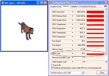
loads. The GPU load application is a set of rotating tigers. Varying the number of tigers
adjusts the GPU load to the desired 25% (200 tigers), 50% (480 tigers), and 75% (2000
tigers). Figure 13 shows this application alongside the measured GPU load of 50% with
480 tigers.
The loads of these applications were determined using Microsoft Perfmon for the
applications were run in parallel with the test code. They produced files containing CPU
loads and GPU loads, respectively. These loads were recorded every second; the average
load over the execution period for each test was calculated based on the values found in
these files. Throughput measurements were made for loads ranging between 0% and 60%
on the CPU and 0% to 75% on the GPU. The throughputs calculated under each load
[image:43.612.93.522.239.540.2]were then compared to the unloaded values.
Chapter 8
Results and Analysis
Before results could be obtained, the algorithms had to be verified for proper
functionality. The documentation available for each algorithm includes a set of standard
test vectors as well as their respective results. These values can be found in [12], [25],
and [26] for AES, SHA-2, and Keccak, respectively. Each algorithm was used to encrypt
or hash the provided test vectors and the resulting output was compared to the provided
result. In all cases, these values were identical signifying a properly functioning
algorithm. Once the algorithms were verified, they were tested to ascertain their
performance.
8.1. Single Kernel GPU Performance
8.1.1 AES
In order to obtain the best performance results, the proper CUDA configuration
had to be determined. This determination required performing the AES encryption on
numerous data sizes while varying the threads per block: 64, 128, 256, and 512 threads
per block were tested. The resulting total throughputs were calculated and graphed as
shown in Figure 14, Figure 15, and Figure 16 for AES-128, AES-192, and AES-256,
respectively. For all three versions of AES, the four configurations of threads per block
performed comparably up to 512 KB. For data sizes greater than 512 KB, the 64 threads
per bock configuration outperformed the rest by as much as 11.4%. Hence, the 64 threads
Figure
Figure
Figure 14: AES-128 Threads/Block Comparison
Using the 64 threads per block configuration, the GPU throughputs and total
throughputs were calculated. These values are graphed in Figure 17, Figure 18, and
Figure 19 for AES-128, AES-192, and AES-256, respectively. They are graphed
alongside CPU throughputs which were obtained from [23]. The total throughput was
lower than the CPU throughput for datasets smaller than 512 KB for AES-256 and
smaller than 1 MB for AES-128 and AES-192. For larger datasets, the GPU throughput
overtakes the CPU throughput approaching approximately 1.9x, 2.3x, and 2.6x faster than
the CPU on 32 MB datasets for AES-128, AES-192, and AES-256, respectively. These
speedups can be seen in Figure 20. This trend is to be expected of CUDA devices which
perform best with large datasets. As discussed earlier, high occupancy is a driving factor
of performance in CUDA GPUs. For AES, occupancy increases as dataset size increases
[image:46.612.92.524.403.691.2]with full occupancy being achieved by 512 KB.
Figure 19: AES-256 Performance
A major bottleneck in the AES performance results is the overhead of data
transmission between the CPU and GPU. When only considering the GPU performance
of AES encryption, speedups as high as 6x over CPU implementations were seen.
The speedups achieved are somewhat slower than those achieved by previous
results. Manavski saw speedups of 5.9x for AES-128 and 5.4x for AES-256 [13].
However, the speedups realized by this thesis are sufficiently comparable for analysis of
CPU and GPU load effects.
8.1.2 SHA-2
Unlike AES, SHA-2 was not parallelizable and ran only in a single thread. As a
result, GPU computation of SHA-2 was not expected to exhibit the performance
increases seen with AES. Figure 21 and Figure 22 illustrate both the GPU performance
and total performance versus the CPU results from EBACS for SHA-256, and SHA-512,
respectively. The CPU outperforms the GPU by a factor of 400 in the case of SHA-224
and SHA-256, and a factor of 510 for SHA-384 and SHA-512. Maximum performance is
achieved at approximately 1KB of data in all four cases. This is the point at which the
encryption time is large enough to mask the effects of transferring data between the CPU
and GPU.
The large performance degradation can be explained by architectural differences
between a CPU and a CUDA enabled GPU. CUDA devices are designed for parallel
processing. A single processing core of a CUDA device is vastly inferior when compared
head to head with a GPU. The power of CUDA lies in the collective ability of all the
cores on the GPU to take advantage of parallelism. Unfortunately, in the case of SHA-2,
Figure 22: SHA-512 Performance
8.1.3 Keccak
Similar to SHA-2, Keccak does not exhibit large amounts of parallelism. The
implementation chosen by this thesis utilized 25 threads, one for each lane of the state.
Once again, this lack of parallelism led to degradation in performance when implemented
on the GPU. CPU results could be found only for Keccak-256; thus, that is the only
comparison available. The CPU version of Keccak-256 outperformed the GPU version by
a factor of 100. These results are illustrated in Figure 23 for Keccak-256. GPU
implementation of Keccak-224, Keccak-384, and Keccak-512 are expected show similar
performance relative to a CPU.
8.2. Multi-Kernel GPU Performance
An additional test to analyze the effects of encrypting multiple datasets in parallel
on a GPU was performed for AES. The speedups produced are highly dependent on
occupancy, or, indirectly, dataset size. For smaller datasets, a single kernel may not be
able to produce full occupancy; thus it may benefit from executing multiple kernels.
Larger datasets, which do produce full occupancy, will see only small benefits as a result
of the pipeling that occurs when executing multiple kernels
The AES encryption was performed 2–4 times in parallel by launching 2–4
kernels simultaneously. The results of these tests can be seen and Figure 24 for AES-256.
Simultaneous encryption produced speedups of 1.3x–1.4x with two kernels, 1.55x–1.65x
with three kernels, and 1.6x-1.8x with four kernels for datasets smaller than 512 KB. This
translates to speedups between 3.6x and 4.7x over CPU implementations of AES. For
datasets larger than 512 KB, using multiple kernels had a much smaller speedup of 1x–
Implementing SHA-2 and Keccak in a multi-kernel way may actually be more
beneficial. As neither SHA-2 nor Keccak produce full occupancy, much of the GPU is
left unused. With a modified version of the current implementations, 240 simultaneous
executions of SHA-2 or 30 of Keccak could be performed simultaneously on a GTX 285
regardless of dataset size.
8.3. Typical System Loading Effects
8.3.1 Offloading Effects
To determine the effects of offloading, the effective CPU time of each GPU
implementation had to be calculated. The effective CPU time is the difference between
the total time and the GPU time. In cases where GPU time could not be accurately
measured, the total time is used as an approximation; this is the case for AES
The effective CPU time was then used to calculate the percentage of CPU time
saved by using a GPU implementation. Like previous results, a performance benefit from
GPU offloading of cryptographic processing was not seen until large enough datasets
were used. For datasets of 256 KB and larger, all versions of the three algorithms saw
time savings from GPU offloading. The largest improvement was seen by AES-256,
which reduced CPU time by 60%. All implementations saw time savings of at least 20%,
and the times savings increased with dataset size up to 50% time saving with a dataset
size of 1 MB. These results are illustrated in Figure 25, Figure 26, and Figure 27 for
AES, SHA-2, and Keccak, respectively.
These results are highly dependent on both the CUDA implementation and the
performance improvements from GPU implementation relative to CPU implementation,
the throughput of the CUDA implementation is the primary factor; the percentage of time
saved can be calculated directly from the speedup as 1 ଵ
௦ௗ௨. However, for
algorithms where a GPU implementation does not reduce execution time, the comparison
becomes somewhat more arbitrary. The only conclusion that can be drawn for these cases
is that some percentage of CPU time will be saved, although how much cannot be
determined for all cases in a systematic way.
[image:52.612.181.430.274.707.2]Figure 27: Keccak Offloading Effects
8.3.2 CPU Load Effects
For GPU processing, the effects of additional CPU loads are highly dependent on
the total time of the algorithm. The primary use of the CPU is for transferring data and
initializing the kernel. Consequently, adding a CPU load has no effect on GPU
processing time. However, total time can be adversely affected.
In cases where total time is low, such as AES, a CPU load may have a significant
negative effect. The effects are illustrated in Figure 28 for AES-256. With a 20% load, an
average degradation of 4% is experienced for datasets larger than 1 MB. Average
degradations of 12% and 22% are experienced with 40% and 60% loads, respectively, for
datasets larger than 1 MB. The precise effects on datasets smaller than 1 MB are difficult
to measure as they are generally encrypted quite fast and are prone to experiencing large
percentage increases and decreases with small variations in performance. However, the
effects on smaller datasets are generally minimal in terms of time. Similar trends were
seen for AES-128 and AES-192 (these results can be seen in Appendix D). The effects of
Figure 28: AES-256 CPU Load Effects
In cases, where total time is high, such as for SHA-2 and Keccak, a CPU load has
a negligible impact because the majority of the total time is from GPU processing. CPU
loading effects are illustrated in Figure 29 and Figure 30 for SHA-512 and Keccak-512,
respectively. For all versions of both SHA-2 and Keccak, 20%, 40%, and 60% loads
produced no degradation in time greater than 1.5% for files larger than 32 KB. Again, the
effects on datasets smaller than 32KB are difficult to measure but are minimal in terms of
time. Similar trends were seen for SHA-224, SHA-256, SHA-384, 224,
Figure 30: Keccak-512 CPU Load Effects
8.3.3 GPU Load Effects
Like the CPU load, the effects of introducing a GPU load are highly dependent on
the time of the alg
![Figure 2: CUDA Thread Hierarchy [5]](https://thumb-us.123doks.com/thumbv2/123dok_us/52529.4784/17.612.153.462.263.662/figure-cuda-thread-hierarchy.webp)
![Figure 3: CUDA Hardware Architecture [4]](https://thumb-us.123doks.com/thumbv2/123dok_us/52529.4784/18.612.90.524.71.312/figure-cuda-hardware-architecture.webp)
![Figure 6: AES State Array [11]](https://thumb-us.123doks.com/thumbv2/123dok_us/52529.4784/24.612.105.511.263.384/figure-aes-state-array.webp)
![Figure 11: Keccak State [20]](https://thumb-us.123doks.com/thumbv2/123dok_us/52529.4784/36.612.211.403.489.687/figure-keccak-state.webp)