Objectives
I ntrodu ct ion to Com put er H ardwareAfter completing this chapter, you should be able to:
◗ Describe the fundamental elements of every computer system: proces-sor, memory, and input/output
◗ Compare elements of the HC11 block diagram to the fundamentals of every computer system
◗ Describe the use of busses to connect computer elements ◗ Explain the three major functional units of a processor ◗ Illustrate the typical registers inside the processor ◗ List the HC11 processor registers
◗ Discuss the HC11 processor modes
◗ Compare and contrast various memory types ◗ Describe the on-chip memory of the HC11
◗ Specify input/output functions present on most computers ◗ Use some basic BUFFALO commands to control the EVBU
Outline
◗ 1.1 Elements of Every Computer
◗ 1.2 Elements of Processors
◗ 1.3 Introduction to Memory
◗ 1.4 Memory Types
◗ 1.5 Input/Output
◗ 1.6 EVBU/BUFFALO
Introduction to Computer Hardware
c h a p t e r
1
Introduction
Computer systems have been developed for a variety of functions and purposes. General-application desktop machines are the most common. They run a variety of software applications, such as word processing, financial management and data processing. They have all but replaced the typewriter as a necessary business tool. Computers are also present in automobiles, appliances, airplanes and all types of controllers and electromechanical devices.
Despite the differences among these computer systems, they all share fundamental components and design. The purpose of this chapter is to provide an understanding of the fundamental components of a computer system. A conceptual presentation regarding the elements of every computer system is made with sufficient detail to establish a foundation for these concepts. The concepts will then be extended to the HC11 hardware.
1.1 Elements of Every Computer
All computers are made up of a group of three fundamental elements: a central processor, memory, and input/output devices. Figure 1.1 shows a block diagram of a computer that includes these three elements. The examination of any kind of desktop computer, workstation or computer control system will reveal at least this minimum structure. Many computing devices will have multiple processors, multiple memory types, and numerous input/output devices. In many cases, the input/output devices contain all three elements as a unit. Video cards for personal computers, for example, always contain a video processor and memory in addition to their inherent input/out-put capability.
Central Processor
(CPU)
Connection to the Outside World Memory
Input/Output Data Bus
Address Bus
Control Bus
Figure 1.1 Fundamental Block Diagram of a Computer
2
HC11 Hardware Block Diagram
The HC11 is a computer system on a single chip that contains the three functional blocks of a computer system. Its internal central processor is a member of the 6800 family of processors; it has on-board memory and sophisticated on-chip input/output capabilities.
The HC11 block diagram is shown in Figure 1.2. This block diagram is specific to the M68HC11E9 version of the HC11. This version of the HC11 is used on the development board (EVBU), as well as in the examples used throughout this text. Three types of memory are included on-chip: RAM, ROM and EEPROM. The HC11 also supports expanded off-chip memory. It contains five on-chip input/output functions, an analog-to-digital converter, and a sophisticated timing system that supports numerous event-driven functions. The address, data and control busses are not shown in this diagram; the processor is connected to the memory and input/output functions inside the HC11 chip in the manner illustrated in Figure 1.1.
Figure 1.2 M68HC11E9 Block Diagram 3
NOTE: Throughout this text, references to the HC11 presume the M68HC11E9 version of the chip; thus, the shorter, more general name “HC11” will be used, unless otherwise specified.
Central Processor
The processor is the device at the center of the machine. It has the responsibility to execute instructions, manipulate data and perform arithmetic functions. It controls and manages the activities of the entire machine. The human brain is the ultimate processor. It can receive and process instructions, process data (like visual images and sounds) and perform arithmetic calculations. However, the human brain is much, much more than a processor because it has the ability to think and to reason. Computer processors cannot think in the same sense.
The term Central Processing Unit (CPU) is used to refer to the main processor in a system. The CPU often works in conjunction with a set of processors to complete a whole system. Modern computers contain additional processors, other than the CPU. They contain video processors, input/output processors, memory controllers, interrupt controllers and math co-processors, to name a few. Since these other processors are subordinate to the central processor, they are often called sub-processors. Many peripheral devices, such as harddrives, printers and video projection systems, have dedicated processors embedded into their control circuitry.
Memory
Memory is a term that refers to any component that stores data and programs used by the processor. Memory can have many forms. There are semiconductor memories, magnetic memories, and optical memories. Semiconductor memories include read only memory (ROM) and read/write memory (RAM). Magnetic memories include floppy disk drives, hard disk drives and tape systems. Optical memories include CD-ROM, DVD and optical disks. A thorough presentation of memory relevant to the HC11 will be provided in chapter 8. Section 1.3 will address concepts of memory that are applicable to all computer systems and a necessary foundation for this study of the HC11.
Input/Output
Input/Output is a term that refers to any subsystem that has the responsibility of receiving data for the processor (input) or sending data out from the processor (output). Input/Output is typically abbreviated as I/O and does not necessarily imply that a particular device has both input and output capability. Typical input devices are keyboards, mice or scanners. Typical output devices are printers and monitors. Typical devices that perform both input and output functions are modems or tape drives. Collectively, all these devices are referred to as I/O devices. The HC11 I/O capability is discussed in detail in chapters 10 through 13.
4
Busses
The processor communicates with the memory and I/O via busses. On a computer, a
bus is a set of two or more conductors that are grouped together to form a parallel information path to and/or from the processor. The bus size, given in bits, is a measure of the number of conductors that can be active simultaneously on the bus. There are three major busses on computer systems: the data bus, the address bus and the control bus.
The data bus is responsible for the transfer of data between the processor and memory or the processor and I/O. It is a bidirectional bus, because data can travel to or from the processor and other devices. Typically, a data bus transfers data in byte widths. Thus, a data bus is an 8-bit, 16-bit or 32-bit bus (1 byte, 2 bytes or 4 bytes wide). The number of bits, or data bus width, also directly correlates with the default processing capacity of the processor. Typically, processors and computers are referred to by the size of their data busses. An HC11 is considered an 8-bit processor because it has an 8-bit data bus and has the default processing capability of one byte. Pentium-based personal computers are 32-bit or 64-bit machines. Thus, they can process four or eight bytes simultaneously.
The address bus is responsible for the transfer of addresses from the processor to mem-ory or to I/O. The address is used to identify specific memmem-ory locations or I/O devices. It is a unidirectional or one-way bus, because processors are the only devices that can create an address for memory or I/O. Typically, an address bus transfers addresses over the bus in double byte widths. Thus, an address bus is usually a 16-bit, 32-bit, or 64-bit bus (2 bytes, 4 bytes or 8 bytes wide). The HC11 uses a 16-bit address bus.
The control bus is responsible for the control signals necessary to interface the various devices within a computer system. This bus is not typically structured as a fixed number of conductors, as are the data and address busses. It is more likely to be a collection of all other signals necessary for proper operation of the system.
Figure 1.3 illustrates how busses might be implemented between an HC11 and some expanded off-chip memory device. This example uses a 16-bit address bus, an 8-bit data bus and two control signals that would be part of a larger system control bus.
5
HC11 Chip
External Memory Device
Address Bus
Data Bus
Read/Write Control
Output Enable
Two signals connected to the memory device that are part of the system control bus
Figure 1.3 Computer Bus Example
Self-Test Questions 1.1
1.2 Elements of Processors
Processors have the job of processing the data within a computer and controlling the overall operation of the system. The basic block diagram of a processor includes an arithmetic logic unit, processor registers and a control unit, as shown in Figure 1.4.
Arithmetic Logic Unit
The arithmetic logic unit (ALU) is responsible for mathematical and logical operations. Most processors support addition and subtraction, logical AND, OR and NOT operations and data shifting. All of these operations are performed in an ALU. The ALU receives data from the processor registers and from external memory via the external data bus. It does not store data, but it returns the result of the operations to the registers or to memory. The ALU is interfaced to a block of processor registers and
6
Connection to the Devices Outside of Processor
Address Data Control
Addresses from Registers
Control to/from Registers
Control to ALU Internal Processor
Data Bus
Processor Registers
Arithmetic Logic
Unit (ALU)
Control Unit Components of the Processor
Figure 1.4 Processor Block Diagram
1. What are the three main hardware components of a computer?
2. What is the function of each of the three hardware components of a computer? 3. What connects the three hardware components and allows the data, addresses
and control signals to move between these components?
to the control block, as shown in Figure 1.4. The HC11 has an ALU that can perform operations on 8-bit and 16-bit data.
Processor Registers
The processor registers are a set of registers needed to perform the instruction execution. The registers are used to temporarily store data and memory addresses, as well as to contain status and control information. These registers are accessible to the user via instructions. A basic register block configuration is shown in Figure 1.5. Each processor will have a unique design that may not include all the registers described here. Often a processor will contain multiple copies of these registers for versatility and enhanced functionality.
Accumulators are special registers directly linked to the ALU to assist with the arithmetic operations. The results of arithmetic operations are stored in an accumula-tor. The size of the accumulators is related to the size of the data bus. If the processor is an 8-bit processor, then it will have 8-bit accumulators. If it is a 16-bit processor, then it will have 16-bit accumulators. Moreover, processors often have the ability to process data of various sizes. For example, an 8-bit processor may also be able to process 16-bit data. If the processor has a 32-bit configuration, it can also process data in 16-bit or even 8-bit words.
The program counter is a processor register that keeps track of the address of the next location in memory that will be accessed. Every processor must have a register that performs the function of a program counter. The program counter is the same size as
7
b7 b0
b15 b0
b15 b0
b15 b0
b7 b0
b15 b0
8-bit Accumulator
16-bit Accumulator
Program Counter
Stack Pointer
Address Register
Status Register
Figure 1.5 Basic Processor Registers
the address bus. If the processor has a 16-bit address bus, the program counter is a 16-bit register. Instructions require one or more bytes of memory for their completion; therefore, the program counter must be capable of incrementing through memory as the instructions are executed. Without the program counter, the processor would not be able to determine which instruction to execute. This register is sometimes called the instruction pointer.
The processor has a need to temporarily store and retrieve data from memory during the processing of instructions. This temporary memory area is called the stack. The processor must have a register that contains an address pointer that indicates the next available memory location on the stack. This register is called the stack pointer. The stack pointer is the same size as the address bus. If the processor has a 16-bit address bus, the stack pointer is a 16-bit register.
Most general-purpose processors contain registers that are used specifically by the instructions to address memory. These registers have various names, but generally they are called address registers. The use of address registers allows for simpler instructions, because they do not need to be concerned about the address. The address required to complete the instruction is already provided in the address register.
Every processor must have a register dedicated to reporting status. The status register
contains bits that indicate certain results of the last operation. The most common status bits are sign flags, carry/borrow flags, zero flags and overflow flags. The sign flags indicate the sign of the last data processed. The carry/borrow flags indicate that an arithmetic operation produced a result larger than could fit into the register used or that it had to borrow to complete the operation. The zero flag indicates that result of the last operation was zero, and the overflow flag indicates that a sign overflow occurred (the sign of the last operation is wrong).
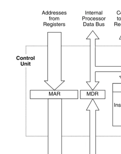
Control Unit
The control unit within the processor is responsible for reading the instruction from memory; it then ensures that the instructions are executed. The control function is driven by the instructions that are decoded by the control unit. The decoded instruction causes a series of steps to be followed during the execution. Figure 1.6 shows the major components of the control unit within a processor.
The memory address register (MAR) is a special address register that is linked to the program counter. The job of the MAR is to contain the address of the current data word that is being addressed. The memory data register (MDR) is another special register that resides between the data bus and the various processor registers. It provides buffering and control of the movement of data into and out of the processor. The MAR and MDR are not accessible to the user, but are used internally by the processor for address and data bus interface and to assist in the execution of instructions.
The instruction register (IR) is a special register that always contains the opcode for the current instruction. This instruction opcode is read from memory during a fetch 8
cycle and deposited into this register. The opcode remains in this register until it is overwritten by the opcode for the next instruction.
Opcodes, operands and instructions are explained in Chapter 2.
NOTE: The instruction register should be called the opcode register, because it contains only the opcode of the instruction. Operands and operand addresses are not processed by the instruction register.
The instruction decoder is the main section of the control block. It has the job of decoding the instruction in the instruction register and controlling the execution of the instruction. It causes each step of the instruction execution to take place. If an address needs to be read from memory, the instruction decoder will cause that to take place. If data needs to be added, it will tell the ALU to perform an addition operation, and so on.
T he process of fetching and executing an instruction is covered in chapter 2.
HC11 Processor
The HC11 is a member of the Motorola 6800 family of processors. It is compatible with
the M6800 and M6801 processors. In addition to executing all M6800 and M6801 9 Connection to the Devices
Outside of Processor
Address Data Control Instruction Decoder
IR MDR
MAR Control
Unit
Addresses from Registers
Internal Processor
Data Bus
Control to/from Registers
[image:10.612.129.334.66.326.2]Control to ALU
Figure 1.6 Components of the Processor Control Block
instructions, the HC11 supports many additional instructions. The HC11 supports 16-bit by 16-bit divide instructions, twelve instructions that support bit-manipulation, and various instructions that support a second address register (Y), none of which was available on the original 6800.
The HC11 MCU is an 8-bit processor, which supports a 16-bit address bus. It contains an 8-bit ALU that can be configured to perform some 16-bit operations.
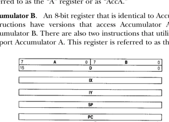
HC11 Processor Registers
The HC11 has a complete set of processor registers. This set of registers is called the
programmer’s model, as shown in Figure 1.7. It has two 8-bit accumulators that can be configured as a 16-bit accumulator for some operations. It has two16-bit address registers, a 16-bit stack pointer and a 16-bit program counter. Finally, it contains an 8-bit status register that contains three control bits and five status flags. None of these registers is addressable as memory; they can only be accessed via instructions. These registers are described in the following sections.
Accumulator A. An 8-bit register that is used as the primary data-processing register. All arithmetic and logical instructions can operate on data in this register. Many special-purpose instructions can only operate on data in this register. This register is referred to as the “A” register or as “AccA.”
Accumulator B. An 8-bit register that is identical to Accumulator A in function. Some instructions have versions that access Accumulator A only and do not support Accumulator B. There are also two instructions that utilize Accumulator B and do not support Accumulator A. This register is referred to as the “B” register or as “AccB.”
10 Figure 1.7 HC11 Programmer’s Model (adapted with permission from Motorola)
[image:11.612.117.404.385.592.2]Accumulator D (A:B). A 16-bit register that is the two 8-bit accumulators joined together (the colon between A and B indicates the joining of the two registers). It is not a separate hardware register. Although the HC11 is technically an 8-bit processor, several instructions are provided that allow 16-bit operations. This joining of A and B is referred to as the “D” register or as “AccD.”
Index Register X. A 16-bit address register that is used by the indexed addressing mode instructions. It can also be used as a general-purpose, 16-bit data register. When used with the indexed addressing mode instructions, it contains a 16-bit base address. When used as a general-purpose data register, 16-bit data of any type can be stored and processed in this register. This register is referred to as the “IX” or simply the “X” register.
T he role of the memory addressing registers is explained in chapter 2 during the presentation on memory addressing modes. T he use of these registers to address memory is emphasized in chapter 5.
Index Register Y. A 16-bit address register that is identical in function to index register X. This register is referred to as the “IY” or simply the “Y” register.
Stack Pointer. A 16-bit register that always contains the address of the next available stack memory location. It is referred to as the “S” or the “SP” register.
T he use of the stack pointer and the function of the memory stack are explained in chapter 6.
Program Counter. A 16-bit address register that always contains the address of the next location in memory that will be addressed. It is referred to as the “PC.”
Condition Code Register. An 8-bit status and control register. Five of the eight bits (H, N, Z, V and C) are status flags, which indicate the results of the last processor operation. The remaining three bits (S, X and I) are control bits for advanced processor functions. This register is referred to as the “C” register, the “CCR” register and the “Status” register.
T he function of the status flags is presented in chapter 3 (Instruction Set). T he function of the control bits is presented in chapter 10 (Interrupts).
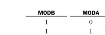
HC11 Processor Modes
The HC11 supports four hardware modes: Single Chip, Expanded, Special Test and Bootstrap. Each hardware mode configures the HC11 to perform a special class of hardware functions.
Single chip mode is the normal operating mode. As the name implies, the single chip mode requires that all software needed to control the processor is contained in the on-chip memories. External address and data busses are not available. Expanded mode
is an alternative normal operating mode. It allows for off-chip memory connection. In this mode, the PORTB and Port C pins are converted to a multiplexed address and data bus. In addition, the strobe A and strobe B control lines become the address strobe and read/write control lines.
Special Test mode is a special mode intended primarily for testing during the chip
production process. The bootstrap mode is another special hardware mode, designed 11
to allow loading of permanent programs and other production related programming tasks.
NOTE: This text focuses only on the normal modes and primarily on operation in the single chip mode. Some examples and explanation of the use of the expanded mode are provided in chapter 8 on memory. The special modes will not be discussed, because of the advanced nature of their function.
The hardware mode is selected by the logic levels on two mode control pins (MODA and MODB) when the processor is in the reset state. Figure 1.8 shows the logic levels required to select each of the four modes. The MODB bits selects between the normal modes (Single Chip and Expanded) and the special modes (Bootstrap and Test).
Self-Test Questions 1.2
1.3 Introduction to Memory
Memory is a term that refers to any component that stores data and programs for the processor. The programs (software), as well as the program data, are stored in the memory during execution and processing. Memory consists of storage locations, where each location can contain one byte of information. A unique address is assigned to each storage location in memory so that it can be individually accessed. The HC11 uses memory that contains a byte of data in each storage location.
A memoryaddress is an n-bit binary number that the processor uses to select a specific memory location. If the processor wishes to communicate with memory location 7, it produces the 16-bit binary address for this location (%0000 0000 0000 0111) and places this address on the address bus. The number of address bits in a system determines the number of unique addresses that can be created by the processor, as shown in 12
MODB MODA Mode
10 Single Chip
11Expanded
0 0 Bootstrap
[image:13.612.175.351.67.127.2]0 1 Test
Figure 1.8 Hardware Mode Select (courtesy of Motorola)
1. What are the three main components of a central processor?
2. What is the function of each of the three components of a processor? 3. What registers make up the M68HC11 programmer’s model?
Equation 1.1. The HC11 uses a 16-bit address. Therefore, it can address 216 or 64K unique memory locations.
# of unique addresses = 2n Equation 1.1 where n is the number of address bits in the system.
Although an address can be generated from each combination of binary bits in the address, there may not be physical memory at all locations in the address range. A
memory map designates the memory addresses that are connected to physical memory locations and indicates which locations are unused. For example, a system may have a 16-bit address bus, which allows it to address 64K memory locations. However, the system may have only 16K of physical memory connected. In this case, the memory map indicates the address range within the 64K range that will be used for this 16K device. Figure 1.9 illustrates how this memory map would look.
The data is the information stored at each memory location. Since all data is just a group of binary bits, it all appears about the same to the processor. It is impossible by simple inspection to know if a value in memory is a number, a special code or a piece of a larger address. The real value of the data is how it is used. The meaning of the data comes from the order in which it appears in the memory, as well as how it is used by the processor.
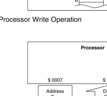
The process of storing data in memory is called a write operation. When a specific memory location is addressed, the data can be written to the data bus by the processor, as shown in Figure 1.10. The processor generates the address $0005 and sends it to the memory device on the address bus. Then the processor places the data $CF on the data bus. The processor tells the memory what type of operation to perform via the control signals. Writing to memory is a destructive
process, which means that any data previously in the memory location is overwritten by the new data and the old data is lost. After a write operation, the data will remain in the memory location until it is overwritten by another write operation.
Data can also move from the memory location to the processor via a read operation,
as shown in Figure 1.11. A read operation causes a copy of the data to be sent to the processor from the memory. The processor initiates a read operation by
placing the address ($0007) on the address bus. It then signals the memory to 13
$0000
16K device
$3FFF $4000
$FFFF
unused
Figure 1.9 Example of Memory Map
place the data ($CE) from the addressed location on the data bus. The processor waits a specific length of time and then reads the data from the data bus. The signal between the processor and the memory that controls the direction of data movement is usually called read/write. Reading from memory is a nondestructive
process, which means that data in the memory location is not affected.
Self-Test Questions 1.3
14
Address Bus
Address is decoded from address bus.
Data is copied from data bus to selected memory location. Data
Bus
R/W Control $ 0005 $ CF
$ CF 6 5 4
0
Processor
[image:15.612.174.356.64.222.2]Memory
Figure 1.10 Processor Write Operation
1. What is an address?
2. How many unique addresses can be generated from a 12-bit address bus? A 20-bit address bus?
3. In which direction does the data move during a read operation?
Address Bus
Address is decoded from address bus.
Data is copied from selected memory location to processor data bus. Data
Bus
R/W Control $ 0007 $ CE
$ CE $ AA $ 86 8 7 6
1
Processor
Memory
Figure 1.11 Processor Read Operation
[image:15.612.174.355.260.423.2]1.4 Memory Types
The physical memory locations can be represented by various types of memory devices. Two different types of memory made from semiconductor materials will be described: volatile and nonvolatile. Volatile memory is a memory that retains the data only when the power is applied. If the power is removed, the data stored in the memory locations will be lost. As the name implies, nonvolatile memory is not volatile. A nonvolatile
memory retains the data with or without power being applied to the device.
RAM
RAM stands for Random Access Memory; however, it is better described as read/write memory. Most memory on modern computers is random access, which means that it can be randomly addressed (the data is accessed in any order the processor chooses). Sequentially accessed memory is used only for special processing and timing applica-tions and will not be described in this text.
RAM is volatile, retaining data only when the power is applied. If the power going to RAM is turned off, all data contained in it is lost. When power is reapplied, the content of RAM is undefined, which means the data can be any value. RAM is used for temporary storage of programs while they are being executed, as well as for temporary storage of data while it is being processed. RAM is relatively fast memory when compared to the whole family of various memory devices. RAM is also relatively less expensive, uses less power and is smaller than most memory devices.
ROM
ROM stands for Read Only Memory. ROM is used for permanent storage of programs and data. It is a nonvolatile memory; therefore, it always retains its data, whether power is applied or not. Standard ROM must be loaded with the permanent programs and data during the manufacturing process. Other types of ROM have been developed that allow programs and data to be written to them after the manufacturing process.
Programmable Read Only Memory or PROM is designed to be programmed in the field, after the manufacturing process. This provides the user the ability to purchase one chip and use it for various purposes dependent upon the field application. PROM can be programmed one time. If a program or data contained in a PROM needs to be modified, the PROM must be discarded and a new one must be programmed.
Erasable Programmable Read Only Memory, EPROM, is a type of PROM that can be erased by applying an intense ultraviolet light to the memory circuitry. Once it has been erased, it can be reprogrammed using a special programming fixture. Chips that contain EPROM have a small window on the chip package that allows the light to reach the memory circuitry. Once an EPROM is programmed, this window is covered to stop light from entering the device and inadvertently erasing the memory locations.
Electrically Erasable Programmable Read Only Memory, EEPROM, can be erased with
electrical signals and then reprogrammed. EEPROM is used in various devices that 15
require permanent memory yet need the convenience of electrical erasure. Single locations within an EEPROM can be erased and reprogrammed.
HC11 Memory
The HC11E9 contains three types of on-chip memory, RAM, EEPROM and ROM, as shown in Figure 1.12. There are 512 bytes of RAM located in the memory map, from $0000 through $01FF. In addition to the RAM, the HC11 contains 512 bytes of EEPROM and 12K of ROM. The EEPROM is located from $B600 through $B7FF in the memory map, and the ROM is located from $D000 through $FFFF. In addition to this memory, a 64-byte register block is located at $1000 through $103F within the memory map.
Refer to chapter 8 for a further presentation regarding HC11 memory.
Self-Test Questions 1.4
1.5 Input/Output
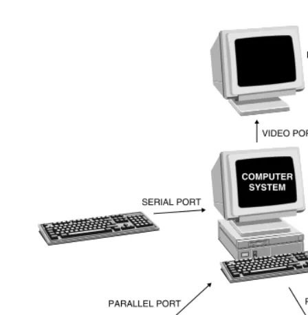
The third element of every computer system is the I/O. All computers must input data from at least one source. The data is processed internally and then output to an external device. Not all I/O capabilities are related to specific devices. For example, most desktop computer systems have general I/O ports. A port is an I/O connection that allows for the movement of data between the computer and an I/O device. There are two major types of ports on computers: serial ports and parallel ports. A serial port is 16
Figure 1.12 Memory Map on the HC11E9
$ 0200 $ 0000
$ 1000
$ B600
SINGLE CHIP $ FFFF $ D000
512 BYTES RAM
64-BYTE REGISTER BLOCK AVAILABLE
FOR EXPANDED
MEMORY
512 BYTES EEPROM
FFFF B600 B7FF
D000 1000
103F 0000
01FF
12 KBYTES ROM $ 0FFF
$ 1040
$ B5FF
$ B800
$ CFFF
1. What two types of memory devices make up the memory system of a computer? 2. What type of ROM can be erased by electrical signals?
3. How much RAM is contained on the HC11E9?
designed to allow two-way transfer of data as a serial data stream. Serial means one bit is transferred at a time over a single wire or line. Modems use serial connections to interface to the computer. High-speed serial ports are becoming the standard for communications. A parallel port is designed to transfer data in parallel. Parallel means multiple bits are transferred simultaneously over multiple wires (typically, 8). Histori-cally, most scanners and printers use parallel ports to interface with the computer.
[image:18.612.116.340.62.291.2]A special type of I/O requires an analog interface. Many data sources in the real world are analog. For the computer to access this data, it must be converted into a digital form, using an analog to digital converter. When the computer needs to send data to an analog device, a digital to analog converter is necessary. Examples of analog data are temperature, wind speed, and humidity.
Figure 1.13 illustrates various I/O devices that may be connected to a computer system.
I/O on the HC11
The HC11 contains several on-chip ports that provide a variety of input/output functions. The I/O capabilities are organized as shown in Figure 1.14.
Port A can be used for digital I/O as well as for multiple timer functions. The digital I/O capabilities include three dedicated output pins, three dedicated input pins and two programmable I/O pins. A 16-bit free running counter is included to support the input-capture and output-compare timer functions. In addition, an 8-bit pulse accumu-lator subsystem and a periodic interrupt generator are provided as part of the Port A
timing system. 17
MONITOR
SERIAL PORT VIDEO PORT
SERIAL PORT
PARALLEL PORT
SCANNER
PRINTER PARALLEL PORT
COMPUTER SYSTEM
Figure 1.13 I/O Devices Connected to a Computer System
See chapter 12 for explanation of the Port A timing system.
Port B is an 8-bit general-purpose output port. Port C is an 8-bit general-purpose port that can be configured for either input or output operation.
T he primary I/O functions of Port B and Port C are presented in chapter 9.
Port D is a general-purpose digital port and also supports serial communication functions. The digital I/O function uses the six I/O pins of Port D as programmable I/O pins. When used for serial communications, two independent serial interfaces can be configured. They are called the serial communications interface (SCI) and the serial peripheral interface (SPI).
T he serial communications capabilities built into Port D are discussed in chapter 13.
Port E is an 8-bit general-purpose digital input port that can be configured as an 8-channel analog-to-digital converter with an internal resolution of 8-bits.
T he analog input capabilities of the HC11 are presented in chapter 11.
[image:19.612.91.439.61.365.2]18
Figure 1.14 HC11 I/O Ports (adapted with permission from Motorola)
Self-Test Questions 1.5
1.6 EVBU / BUFFALO
A full explanation of the function of the EVBU is presented in the Universal Evaluation Board User’s Manual. Refer to section 4.6 of the EVBU User’s Manual for a description of the BUFFALO monitor commands.
The EVBU is the Motorola M68HC11 Universal Evaluation Board. It is a development tool for HC11 microcontroller-based designs. It provides a variety of features with which to experiment with the functions of the HC11 and to test designs based on the HC11. It also works well as an educational tool. In addition to the HC11 chip, the EVBU contains the following hardware features:
◗ M68HC68 Real-time clock chip. The real-time clock chip provides accu-rate timing information in seconds, minutes, hours, and so on.
◗ Standard serial communications port. This port allows connection to an external computer.
◗ Breadboard area. A small solder pad development area is provided on the EVBU layout.
The EVBU has a monitor program that serves as an operating environment. The
monitor program is a piece of software that provides a controlled environment in which the HC11 can operate. It also provides a user interface (UI). The UI allows a user of the EVBU to enter some simple commands to access memory, run programs and monitor the function of the HC11. The monitor program is called BUFFALO (Bit User Fast Friendly Aid to Logical Operations). BUFFALO works in conjunction with the EVBU hardware to provide the following features:
◗ One-line assembler. The user can enter programs directly into memory. ◗ Program download. Programs that have been created externally can
be loaded directly into memory.
◗ Troubleshooting capabilities. BUFFALO commands allow users to exe-cute programs one step at a time, to stop programs at a particular in-struction and to examine the contents of the registers and memory.
BUFFALO is burned into the HC11 on-chip ROM during the manufacturing process. It occupies 8K of the 12K of available ROM. In addition, some of the RAM is used by BUFFALO as system temporary memory. Therefore, only part of the RAM is available
for user programs and data. However, the EEPROM is unused by the EVBU and is 19 1. What is a port?
2. What is the difference between a serial and a parallel port? 3. Why are analog interfaces needed?
4. How many I/O ports are contained on the HC11? What are they?
available for user programs. The ROM on the EVBU contains the system control program.
NOTE: BUFFALO is located in the on-chip ROM from $E000 through $FFFF. It uses some of the on-chip RAM as temporary memory. User programs must not use RAM between $0030 and $00FF, to avoid conflicts with the system temporary space.
A photograph of the EVBU is shown in Figure 1.15. The block diagram of the EVBU is shown in Figure 1.16.
20
Figure 1.15 EVBU Photo
PA0-PA7 PD0-PD5
PD2-PD5 XIRQ PE0-PE7
TXD/PD1
TERMINAL
BATTERY BACKUP HC11
RS-232C DRIVERS AND RECEIVERS
REAL-TIME CLOCK,
RAM, SERIAL INTERFACE PB0-PB7
RXD/PD0
TXD RXD
PC0-PC7
CONTROL
Figure 1.16 EVBU Block Diagram
Basic EVBU Function
The BUFFALO monitor program controls the HC11 within the environment created by the EVBU hardware. The user can type commands at the BUFFALO prompt that tell BUFFALO to perform a variety of memory operations and control functions. For example, BUFFALO provides a command that allows the user to display a block of memory to the screen. This command is called Memory Display and is abbreviated by using the letters MD followed by the address range that will be dumped to the screen. The operation of this instruction is shown in Figure 1.17. The user types in the MD command at the BUFFALO prompt, followed by the start and end addresses of the range to be displayed (in this case $E640–$E68F). Note that hex is assumed for the addresses that are supplied with the BUFFALO command. Thus, the user should not use the preceding “$” character to indicate hex. Then BUFFALO displays values stored in memory for this range. Each row of the output contains the start address or the address of the first byte displayed, followed by the hex values for the data stored in 16 sequential memory locations. At the end of the line, the ASCII equivalent characters are displayed for each value shown on the line (i.e., $42 = “B”, $55 = “U”, $46 = “F,” etc.). When the display is complete, a new BUFFALO prompt is displayed, prompting the user for another BUFFALO command.
T he concepts of ASCII communications and use of ASCII characters are presented in Chapter 13.
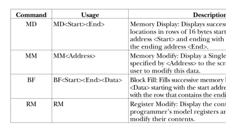
Rather than display all the commands supported by BUFFALO and the EVBU at this point in the text, a brief summary of several useful commands is provided in Figure 1.18. The four commands listed in this table are used to display and change the data in the memory and processor registers in the HC11. They are very useful from the beginning of the study of the HC11 and will be used in the problems at the end of this chapter.
The following examples are provided to show the operation of these instructions.
A complete list of BUFFALO commands is provided in section 3 of the EVBU User’s Manual.
21 > MD E640 E68F<cr>
E640 42 55 46 46 41 4C 4F 20 33 2E 34 20 28 65 78 74 BUFFALO 3.4 (ext E650 29 20 2D 20 42 69 74 20 55 73 65 72 20 46 61 73 ) – Bit User Fas E660 74 20 46 72 69 65 6e 64 6c 79 20 41 69 64 20 74 t Friendly Aid t E670 6f 20 4C 6f 67 69 63 61 6C 20 4F 70 65 72 61 74 o Logical Operat E680 69 6F 6E 04 57 68 61 74 3F 04 54 6F 6F 20 4C 6F ion What? Too Lo >
Figure 1.17 Operation of the MD Command in BUFFALO
Example 1.1
Problem: Use the BUFFALO monitor commands to load a range of memory ($0000–$000F) with $20 and then display the range of memory on the monitor. Solution: This problem requires the use of two BUFFALO commands: BF and MD. First, BF will be used to fill the range with the value $20, and then the MD command will be used to display this on the monitor. The part that is typed by the user is bolded.
> BF 0000 000F 20 <cr>
> MD 0000 000F<cr>
0000 20 20 20 20 20 20 20 20 20 20 20 20 20 20 20 20
>
Example 1.2
Problem: Use the BUFFALO monitor commands to modify the data stored in memory location $0003 so that it contains $FE and then to display the range of memory ($0000–$000F) on the monitor.
Solution: This problem requires the use of two BUFFALO commands: MM and MD. First MM will be used to modify the value at $0003 to $FE, and then the MD command will be used to display a range on the monitor. The part that is typed by the user is bolded.
> MM 0003<cr>
0003 20 FE<cr>
> MD 0000 000F<cr>
0000 20 20 20 FE 20 20 20 20 20 20 20 20 20 20 20 20
>
22
CommandUsage Description
MD MD<Start><End> Memory Display: Displays successive memory locations in rows of 16 bytes starting with the start address <Start> and ending with the row that contains the ending address <End>.
MM MM<Address> Memory Modify: Display a Single byte of memory specified by <Address> to the screen and allow the user to modify this data.
BF BF<Start><End><Data> Block Fill: Fills successive memory locations with the data <Data> starting with the start address <Start> and ending with the row that contains the ending address <End>. RM RM Register Modify: Display the contents of the
[image:23.612.79.455.65.275.2]programmer’s model registers and allow the user to modify their contents.
Example 1.3
Problem: Use the BUFFALO monitor commands to display the data stored in the processor registers. Modify the contents of the X register to be $1000 and AccA to be $3B. Redisplay the contents of these registers to verify that the changes took place.
Solution: This problem requires the use of one BUFFALO command: RM. First RM will be used to display the register contents and modify the values in the X register and AccA. Then the RM command will be used again to display the contents and verify that the changes took place. The part that is typed by the user is bolded.
> RM<cr>
P-0100 Y-FFFF X-FFFF A-FF B-FF C-D1 S-0041
P-0108<SPACE BAR>
Y-FFFF<SPACE BAR>
X-FFFF 1000<SPACE BAR>
A-FF 3B<cr>
> RM<cr>
P-0100 Y-FFFF X-1000 A-3B B-FF C-D1 S-0041
>
Self-Test Questions 1.6
Summary
All computer systems consist of three major components: processor, memory and I/O. The processor is the controlling element of the system. It manages the movement of data to and from the memory and I/O components. The processor is also made up of three major components: ALU, internal registers and control block. The ALU is responsible for the arithmetic and logical functions performed by the processor. The registers provide temporary storage of data and addresses for efficient processing, and the control block manages the execution of the instructions. Memory contains the programs and data used by the processor. Two major types of memory are represented in computer systems, RAM and ROM. Finally, all computer systems must have some connection to the external world. These connections are accomplished by the I/O capabilities. A keyboard is an example of a standard input device, and a monitor is an
example of a standard output device. 23
1. What is the EVBU?
2. What is the name of the monitor program on the EVBU?
3. Which BUFFALO monitor command is used to fill a range of memory locations with a particular value?
Chapter Questions
Section 1.1
1. What are the three major components of a computer system? Why are all of the components necessary in an operational computer system?
2. How does the HC11 meet the functional components of a computer system (processor, memory and I/O)?
3. How are address, data and control signals connected to the various components within the computer system?
Section 1.2
4. What is a processor? What function does a processor perform? 5. What are the sections of a processor?
6. What is the purpose of the ALU?
7. List the common register types in a microprocessor. What purpose does each of the registers have, generally?
8. Does the Control Unit contain any registers? If so, how are they different from the registers in the processor?
9. What kind of processor is embedded in the HC11 microcontroller? 10. How many bits of data can be processed at a time by the HC11 processor? 11. What is in the HC11 programming model?
12. Does the HC11 support different hardware modes? What are they?
Section 1.3
13. If a system has a 20-bit address bus, how many unique addresses can be addressed?
14. What is a memory map?
15. What is the size of the HC11 address bus? What is the maximum number of memory locations that can be addressed by the HC11?
16. If a system has a 16-bit address bus and must address two 32 Kbyte memory chips, draw a picture of how the memory map would be configured to uniquely address each location within the memory devices.
17. How does the processor communicate to memory whether it wishes to perform a read or a write operation?
18. Why is reading memory nondestructive to the data in the addressed memory location?
19. Why is writing to memory destructive to the data that was originally in the addressed memory location?
Section 1.4
20. Explain the differences among ROM, EPROM and EEPROM. 21. Why must every computer system have some nonvolatile memory? 22. What types and quantities of memory are on the M68HC11E9?
23. Is the entire address space used by the on-chip memory on the HC11? If not, how much address space is available?
Section 1.5
24. What types of ports are typically available on computer systems? 24
25. How many ports are available on the HC11?
26. What types of I/O functions are supported by the ports on the HC11?
Section 1.6
27. What is the EVBU? What is its purpose? 28. What is BUFFALO? What is its purpose?
29. How many parameters are used by the BF command?
Answers to Self-Test Questions
Section 1.1
1. Processor, memory and I/O
2. The processor is at the center of the computer. The processor manipulates the data, performs arithmetic functions and manages the processes. The memory is used to store data and programs. The I/O is used to move data to/from the computer and external devices.
3. Busses. The address bus transfers address information from the processor to the memory and I/O devices. The data bus is a bidirectional bus that transfers data to/from the processor, memory and I/O. The control bus is a collection of control signals necessary to control the processes of the computer.
Section 1.2
1. Arithmetic logic unit (ALU), the register block and the control block.
2. The ALU has the job of performing the actual arithmetic data processing. It can do arithmetic and logical operations. The register block contains a set of registers that are used by the processor to store data temporarily, accumulate data, manipulate addresses, and so on. The control block decodes instructions and generates all of the timing and control signals necessary to execute the instructions.
3. The HC11 programming model contains two 8-bit accumulators (A and B) that can be configured as a 16-bit accumulator (D); two address registers (X and Y); a stack pointer (SP), which contains the address of the next available stack location; the program counter (PC), which contains the address of the next instruction to be executed; and the condition code register (CCR), which contains three control bits and five status flags.
Section 1.3
1. An n-bit binary number that the processor uses to select a specific memory location.
2. 12-bit bus →n = 12, therefore 2n = 212 = 4K addresses can be generated. 20-bit bus → n = 20, therefore 2n = 220 = 1M addresses can be generated. 3. The data moves from the memory to the processor during a read operation.
Section 1.4
1. Volatile and nonvolatile, or RAM and ROM. 2. The EEPROM is electrically erasable.
3. There are 512 bytes of RAM on the HC11E9. 25
Section 1.5
1. A port is an I/O connection that allows data to move between the computer and a variety of peripheral devices.
2. A serial port transfers data one bit at a time on a single wire. A parallel port transfers data multiple bits at a time via multiple wires.
3. Analog interfaces are required because most things in the real world are analog. Examples of analog data are temperature, wind speed, humidity and time. 4. There are five I/O ports on the HC11: PORTA, PORTB, PORTC, PORTD and
PORTE.
Section 1.6
1. The EVBU is the HC11 Universal Evaluation Board.
2. The monitor program on the EVBU is called BUFFALO (Bit User Fast Friendly Aid to Logical Operations).
3. The BF command allows a range of memory locations to be filled with the data value given in the command (i.e., BF 0006 001D 40 will fill $0006–$001D with the value $40).
26
Objectives
I ntrodu ct ion to Com put er So ftwareAfter completing this chapter, you should be able to:
◗ Describe the difference between source code and machine code ◗ Define opcode, operand and address of an operand ◗ Explain the purpose of memory addressing modes ◗ Show how memory addressing modes work on the HC11
◗ Explain how an instruction is fetched from memory and executed by the processor
◗ Use flowcharts to show the flow/function of a program
Outline
◗ 2.1 Programming the Computer
◗ 2.2 Memory Addressing Modes
◗ 2.3 HC11 Memory Addressing Modes
◗ 2.4 Processing Instructions
◗ 2.5 Program Flow
Introduction
The programs that run on computers are called software. The software consists of ordered sets of instructions that tell the hardware what it should do. The computer hardware will not function without the software controlling each function. The instructions control the processes that are executed, the data that is processed and the
Introduction to Computer Software
c h a p t e r
2
order in which these operations are completed. This chapter will introduce some concepts behind the software that controls the hardware.
2.1 Programming the Computer
A program is a detailed list of steps that must be followed to complete a task. Many jobs in life follow the same steps each time they are accomplished. Someone who gets up in the morning to go to work often follows a specific set of steps to prepare for work. Cooking a meal from a recipe requires following a set of instructions in a specific order. Most tasks become so natural that the fact that specific steps are followed is forgotten.
Programs tell computers what to do. When the tasks become more complex, more instructions are required to accomplish the task. Unlike humans and animals, computers do nothing except what they are told by the programs. In fact, they do only what they are told. In this sense, they are 100% obedient. They never complain and never have to be fed. They definitely can’t think. The strength of computers comes from the fact that they perform many very simple instructions millions of times a second to accomplish much greater tasks.
Some computers are designed to execute only one program. For example, the computer embedded in the transmission controller on a minivan executes one program. The job of this computer is to control the shifting of the automatic transmission. It has one program or set of instructions. Each time the computer is activated when the car is turned on, it begins to execute the set of instructions that controls the automatic transmission. It knows of nothing else, cares about nothing at all and never complains about its job. This type of computer is a dedicated computer. Many computers are more general in nature. They are designed to allow a variety of programs to be executed. In some cases, they even allow multiple programs to be executed at the same time. Desktop personal computers, for example, are designed to run word processors, e-mail programs, spreadsheets and essentially any program that someone can conceive and write. This type of computer is a general-purpose computer.
Source Code
Source code is a program written in a programming language. Programming languages
are made up of English-like words that communicate the instructions to the computer. Hundreds of programming languages have been developed for this purpose. Program-ming languages are designed to help humans with the process of programProgram-ming computers. Programs written in computer languages must be converted into machine code and loaded into the computer memory. Figure 2.1 shows the relative spectrum of computer languages and provides some samples of how the code might read.
High-level languages are designed to be more removed from machine code and more like a spoken language. They have syntax similar to sentence structure, making them even easier to read. In a high-level language, single keywords can cause many machine-level instructions to be executed. Examples of high-level languages are BASIC, 28
FORTRAN and COBOL. High-level source code must be processed by a program called a compiler or interpreter. It translates the high-level language to the machine-level code that can be loaded into the processor on the target computer.
Assembly is the lowest level of all computer languages. Assembly language program-ming is a low-level programprogram-ming language because it is most like the actual machine code. Assembly language source code is made up of a set of abbreviations, which are specific to a processor or processor family. The abbreviations are called mnemonics (pronounced ne-mon-icks). A mnemonic correlates to a single machine code instruc-tion. The mnemonics are designed to be easy to read and easy to remember. They are a significant improvement over the binary machine codes. The assembly language source code is processed by a program called an assembler, which translates the mnemonics into the machine-level code that can be loaded into the computer.
In addition to low-level and high-level languages, some languages are in between. They are in between because they have characteristics of both types. These mid-level languages have features similar to those of the low-level languages, yet maintain the strengths of the high-level languages. Some examples of languages that fit this description are “C”, “C++” and FORTH.
High-level and mid-level languages have an advantage. The same source code file written in a high- or mid-level language can be compiled to run on almost any hardware. This type of source code is called portable. Because assembly-level languages are so close to the actual machine code, portability is limited to processors within the same family. In most cases it is not portable at all.
On the other hand, low-level languages also have an advantage. Since the low-level source code is so similar to the actual machine code, assembly-level programming tends to result in machine code that is smaller and consequently runs faster than the same programs written in a higher-level language.
Highest Level BASIC Lowest Level MACHINE CODE Relative Level of Programming Language
C BASIC
ENGLISH ASSEMBLER MACHINE
if (X == Y) Z = X; else Z = Y; if (X == Y) then
Z = X else Z = Y end if if X is equal
to Y, then set Z equal to X, otherwise set Z equal to Y
96 00 91 01 27 02 96 01 97 02 X Y PAST Y Z LDAA CMPA BEQ LDAA PAST STAA
C ASSEMBLER
Figure 2.1 Various Levels of Computer Code
29
Machine Code
There is only one language that the computer hardware understands, machine language. The machine language is made up of machine code. The machine code is multibit binary codes that tell the computer the specific tasks it is to perform. Machine code is the lowest level of all computer languages. In general, it is very difficult for humans to communicate with computers solely using machine language. The groups of 1’s and 0’s tend to look alike, and the probability of error is very high. Other computer languages have been developed to aid humans when they program computers.
NOTE: Machine code is commonly referred to as object code, and a machine code program is referred to as an object code program. Because the term “machine code” implies low-level codes that the machine uses, it will be used exclusively in this text. To avoid confusion, the term “object code” will not be used in this text.
The machine code consists of operational codes (opcodes), operands (data) and addresses of the operands. The assemblers and compilers produce the machine code from the lines of code written in the programming language.
An opcode is a multibit code that identifies an instruction. Each opcode contains specific information about the instruction to be executed, as well as how to execute it. Many instructions can be implemented in a variety of ways on a computer. Each method requires a unique opcode; thus, a single instruction will be implemented with one or more opcodes.
An operand is data that is operated upon by the instruction. For example, an addition instruction adds operands, and a load instruction reads an operand from an address in memory and loads it into a processor register. The operand field is a group of up to three bytes following the opcode. The operand field contains bytes necessary to complete the instruction. It can contain 8-bit and 16-bit data, 8-bit addresses and 16-bit addresses. In some cases, the operand field contains nothing at all, because all necessary data is already in the processor registers.
NOTE: The term “operand” is not consistently used throughout computer literature and is often used to refer to any bytes that occupy the operand field. This text will use the term operand in its literal sense, as the data that is operated upon by the instruction. This usage is consistent with the Motorola HC11 data manuals. Addresses and offsets will not be referred to as operands in the text, although they all occupy bytes in the operand field and are commonly referred to this way.
An address is a pointer into memory. Each memory location has a unique address by which it is identified. Most small computers have a byte-oriented memory; therefore, each address points to the location of a byte of data in memory. Addresses can be expressed in an absolute sense. An absolute address is a complete address, or an address that consists of all the address bits. Addresses can also be expressed as an offset. An
offset is a value that is added to a base address to reference another memory location. 30
Offsets are commonly used to allow addressing of memory without specific reference to the entire address. Programs that use offsets typically result in less actual machine code because the offsets are smaller than complete addresses. Since these programs occupy fewer bytes of memory, often they will execute faster.
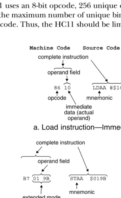
HC11 Machine Code
HC11 machine code is made up of opcodes, operands and addresses. The HC11 uses an 8-bit opcode and supports various ways of accessing operands in memory. Figure 2.2 illustrates three examples of the relationship of the opcode to the bytes in the operand field. Further examples of the relationship of opcodes, the operand field, operands and mnemonic instructions will be provided in sections 2.3 and 2.4 of this chapter.
Since the HC11 uses an 8-bit opcode, 256 unique opcode values can be generated (28 = 256). This is the maximum number of unique binary values that can be derived from an 8-bit binary code. Thus, the HC11 should be limited to 256 instruction opcodes, yet
31
Machine Code
complete instruction
operand field
opcode mnemonic immediate data (actual
operand)
Source Code Comments
86 10 LDAA #$10 ;$A8 ⇒ A
1B ABA
operand field empty
opcode
complete instruction
;(A) + (B) ⇒ A B7 01 9B STAA $019B
mnemonic operand field
extended mode effective address
complete instruction
[image:32.612.133.327.268.584.2];(B) ⇒ $019B
Figure 2.2 Opcode and Operand Field Examples
a. Load instruction—Immediate mode
c. Add instruction—Inherent mode b. Store instruction—Extended mode
the HC11 has 308. The designers of the HC11 built in a mechanism that allows for each of the 308 instruction opcodes to be properly handled. Some of these instructions require an additional opcode byte, which is called a prebyte. The prebyte directs the instruction decoder to perform two fetch cycles. Three of the opcodes are actually opcode prebytes: $18, $1A and $CD. Thus, every instruction that uses a prebyte also has an additional opcode. Appendix C provides a complete listing of all opcodes and prebytes used on the HC11.
Self-Test Questions 2.1
2.2 Memory Addressing Modes
An addressing mode is a method of accessing operands. The addressing mode defines how the instruction will be coded and how it will operate to access and process data. Many instructions can operate in different modes, yet some operate only in a single mode. The addressing mode also defines how the effective address of an operand will be generated. The effective address is the address of the operand in memory. Each addressing mode accesses the effective address in a different manner. For example, the effective address for an immediate mode instruction is the address of the data following the opcode. Furthermore, an indexed mode instruction must calculate the effective address from the contents of the index register and the 8-bit offset provided in the instruction.
T he application of the addressing modes on the HC11 is presented in section 2.3.
Methods of Addressing Memory
Every memory location in memory has a unique address. When data is needed from memory to complete an instruction, the processor generates the effective address and accesses the data stored at that location. There are many methods used by most computers to produce the effective addresses of data in memory. Five methods will be described in the following sections.
Immediate
Immediate addressing is used when the operand immediately follows the instruction opcode in memory. Thus, the memory access is limited to those locations immediately following the instruction opcode.
A number may be needed in a processor to complete a set of instructions. If this number is always the same value, it could be easily loaded into the register using the 32
1. What is a computer program?
2. What is the difference between source code and machine code? 3. What is the operand and how is it used?
4. What is an opcode prebyte?
immediate mode. The number actually resides in the memory location immediately following the instruction opcode, as shown in Figure 2.3.
Absolute
Absolute addressing is used to access the operand directly from memory. The address of the operand follows the instruction opcode in memory. This mode is implemented on different processors in several forms.
Assume for a minute that an operand is in memory location $0012. This address would follow the instruction opcode in memory. When the instruction is executed, the address is retrieved from the memory and then used as the address of the operand. Additional machine cycles must be executed to then retrieve the actual operand that is processed, as shown in Figure 2.4.
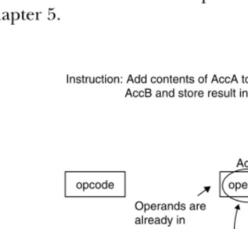
Implied
In implied addressing, no address is necessary because the location of the data is implied by the instruction. For example, if data already exists in two separate accumulators in the processor, this data can be directly added without accessing memory. The instruction that would be used to add the contents of these two accumulators together would be im-plemented in the implied mode, since the data is implied as shown in Figure 2.5. Because the data is already provided in the two accumulators, the data does not need to be retrieved from memory before the addition operation is completed. The instruction is inherently complete, by itself.
Indexed
Indexed addressing uses an address in a register called an index register combined with an address offset to determine the location of the operand in memory. The
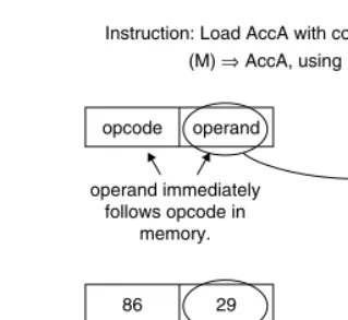
opcode operand
AccA Instruction: Load AccA with contents of memory (M) ⇒AccA, using immediate addressing
operand immediately follows opcode in
memory.
86 29 29
AccA
[image:34.612.148.308.74.221.2]IR receives this code—decoder causes next byte to be loaded into AccA.
Figure 2.3 Loading AccA Using Immediate Addressing
33
instruction indicates which register to use, and the address offset follows the instruction opcode in memory. The address of the operand is calculated by adding the address offset to the address from the index register or by indexing the base address contained in the register. This addressing mode allows for simple access to data stored in a table. A detailed presentation of the HC11 implementation of indexed addressing mode is provided in chapter 5.
34
opcode address
operand Operand is located in memory at address supplied by instruction
M
AccA Instruction: Load AccA with contents of memory
(M) ⇒AccA, using absolute addressing
address of operand
B6 $0120 29
29 $0120
AccA
[image:35.612.178.361.93.242.2]IR receives this code—decoder causes address M to be retrieved, then actual operand to be loaded into AccA from (M).
Figure 2.4 Loading AccA Using Absolute Addressing
opcode operand operand
+
AccB AccA
Instruction: Add contents of AccA to contents of AccB and store result in AccA.
Operands are already in processor registers so no memory accessing is necessary.
1B 29
6C 43
+
AccB AccA
IR recieves this code— decoder causes contents of A to be added to contents of B and stores result in A.
Overwrite 29 with 6C in A
[image:35.612.176.351.432.593.2]