This is a repository copy of
All-optical polariton transistor
.
White Rose Research Online URL for this paper:
http://eprints.whiterose.ac.uk/84437/
Version: Accepted Version
Article:
Ballarini, D., De Giorgi, M., Cancellieri, E. orcid.org/0000-0002-4099-2716 et al. (6 more
authors) (2013) All-optical polariton transistor. Nature Communications, 4. 1778. ISSN
2041-1723
https://doi.org/10.1038/ncomms2734
[email protected] https://eprints.whiterose.ac.uk/ Reuse
Unless indicated otherwise, fulltext items are protected by copyright with all rights reserved. The copyright exception in section 29 of the Copyright, Designs and Patents Act 1988 allows the making of a single copy solely for the purpose of non-commercial research or private study within the limits of fair dealing. The publisher or other rights-holder may allow further reproduction and re-use of this version - refer to the White Rose Research Online record for this item. Where records identify the publisher as the copyright holder, users can verify any specific terms of use on the publisher’s website.
Takedown
If you consider content in White Rose Research Online to be in breach of UK law, please notify us by
All-optical polariton transistor
D. Ballarini1,2, M. De Giorgi1,2, E. Cancellieri3, R. Houdré4, E. Giacobino5, R. Cingolani1, A. Bramati5, G. Gigli1,2,6, D. Sanvitto1,2
1
Istituto Italiano di Tecnologia, IIT-Lecce, Via Barsanti, 73010 Lecce, Italy.
2
NNL, Istituto Nanoscienze - CNR, Via Arnesano, 73100 Lecce, Italy.
3
Fisica Teorica de la Materia Condensada, Universidad Autonoma de Madrid, Spain.
4
Institut de Physique de la Matière Condensée, Faculté des Sciences de Base, bâtiment de Physique, Station 3, EPFL, CH-1015 Lausanne, Switzerland
5
Laboratoire Kastler Brossel, Université Pierre et Marie Curie-Paris 6, École Normale Supérieure et CNRS, UPMC Case 74, 4 place Jussieu, 75005 Paris, France.
6
Innovation Engineering Department, University of Salento, Via Arnesano, 73100 Lecce, Italy.
While optical technology provides the best solution for the transmission of information, all-optical
devices must satisfy several qualitative criteria to be used as logic elements. In particular,
cascadability is difficult to obtain in optical systems, and it is assured only if the output of one stage is
in the correct form to drive the input of the next stage. Exciton-polaritons, which are composite
particles resulting from the strong coupling between excitons and photons, have recently
demonstrated huge non-linearities and unique propagation properties. Here we demonstrate that
polariton fluids moving in the plane of the microcavity can operate as input and output of an
all-optical transistor, obtaining up to 19 times amplification. Polariton propagation in the plane of the
microcavity is then used in turn to control the switching of a second, spatially separated transistor,
demonstrating the cascadability of the system. Moreover, the operation of the polariton transistor as
an AND/OR gate is shown, validating the connectivity of multiple transistors in the microcavity plane
and opening the way to the implementation of polariton integrated circuits.
Light beams can carry information over long distances, and have proved to be better than electronic
wires for low-loss transmissions at high data rate. Moreover, optical connections can, in principle,
operate faster and with lower energy consumption than electronic ones even at very short distances,
down to chip interconnects [1, 2] with the not negligible advantage of having very low dissipations and
virtually no heating. However, the implementation of high-speed, low-energy, optical logics in all-optical
been proposed and studied to develop all-optical switches, only to cite some: Mach-Zehnder
interferometers in semiconductor materials [4], spin polarization in multiple quantum wells [5],
waveguide-coupled ring resonator in silicon [6], photonic crystal nanocavities [7] and polarization
bistability in vertical cavity emitting structures [8]. However, to be used as a logic element in an
integrated circuit, a switch must satisfy some critical conditions such as cascadability (the output and
input should be compatible to allow for connections in series of several devices) and the possibility to
feed with one output several inputs (fan-out or gain) and viceversa (fan-in). [9, 10].
In this context, microcavity polaritons, the quantum superposition of electron-hole pairs (excitons) and
light (photons), are a peculiar and interesting kind of semiconductor quasi-particles. In fact, polaritons
inherit from their photonic part the very light mass (10-4 times that of an electron) and high speed (1% of
the speed of light), which yields fast switching times [11], while their electronic component provides
strong nonlinear effects at power thresholds orders of magnitude lower than in standard dielectrical
optical crystals[12-25]. In the last years, the observation of a non-equilibrium condensed phase [26, 27]
of polaritons paved the way to the study of new quantum phenomena which could lead to virtually
loss-free operations and communication [28-32] up to room temperature [33]. Their potential use for logic
operations has also been explored in recent proposals [34, 35], where the information is carried by
polariton quasi-particles propagating inside the plane of the microcavity along integrated circuits based
[36]. On the other hand, lateral confinement of flowing polaritons has been
realized by modelling the photonic potential of the cavity through precise etching of the structure,
obtaining propagation distances of more than 200 microns [37].
In this Article we experimentally demonstrate the working principle of a polariton transistor in
semiconductor planar microcavities based on the nonlinear interactions between two polariton fluids.
The power threshold for nonlinear absorption of a polariton state (Address) is tuned by the injection of a
small polariton population (Control), showing a ratio between Address and Control densities of more
than one order of magnitude (12dB). We show that the output of one transistor is a polariton fluid
propagating in the plane of the microcavity, which is in the correct form to work as a Control signal for
the switching on of a second, spatially separated, transistor, therefore demonstrating the cascadability
of the system. Moreover, the functionality of the polariton transistor is further extended through the
implementation of the AND and OR gates, where two propagating polariton fluids are used as inputs for
Results
Experimental configuration. Our experiments have been performed in transmission configuration and
at a temperature of 10 K. A sketch of the experimental configuration is reported in Fig.1a: a single mode,
continuous wave, laser beam impinges on a GaAs/AlAs microcavity, composed by front and back
Distributed Bragg Reflectors (DBR) with 21 and 24 pairs respectively, and three In0.04Ga0.96As quantum
wells embedded in the microcavity plane. The laser beam is partially reflected from the front DBR, which
only allows the penetration of those frequencies that match with the polariton dispersion (shown in
Fig.1b). The angle of incidence of the laser beam with respect to the direction perpendicular to the
sample corresponds to the in-plane momentum of the resonantly created polaritons, which propagates
with a finite velocity in the microcavity plane (downward direction in the sketch of Fig.1a). Due to the
finite polariton lifetime in the microcavity (around 10ps), this process can be observed through the
photon emission from the back DBR: the polariton density in each state is proportional to the emission
intensity, which is recorded both in real and momentum space by a CCD coupled to a spectrograph and
directly measured by a power meter. In the experiments described in the following, we used linear
polarized beams to avoid the effect of the spin on the dynamics of the system. Although the additional
degree of freedom constituted by the polariton spin can be advantageous in future devices [38], we will
focus here on the demonstration of the basic transistor operation and its connectivity.
Blueshift mechanism. An important mechanism which plays a key role in this resonant scheme is the
renormalization of the polariton energies with increasing polariton densities. Due to the
polariton-polariton interactions, originated from their excitonic components, the polariton-polariton resonance is indeed
shifted towards higher energies when the polariton density increases. In the case of optical excitation, if
the pumping laser is slightly detuned above the polariton resonance, two different regimes can be
distinguished. For low enough polariton densities, the laser remains out of resonance ( ),
while for densities above a certain threshold the polariton energy jumps into resonance with the pump
energy, resulting in a dramatic increase of the population of the pumped state. This behavior is shown in
Fig.1c for the polariton state called Address in this work and described in the following subsection. On
the contrary, if the pumping laser is set at resonance with the polariton energy, the polariton density
increases linearly until absorption is saturated by the pump-induced blueshift. This is the case for the
Address and Control state. In the first part of the experiment we create both Address and Control states
by external optical injection, measuring the polariton density in the Control needed to switch on the
Address. The laser beam has been divided in two paths, which impinge with different angles on the
microcavity plane in order to resonantly excite two states of the lower polariton branch, Control and
Address, which share the same energy, , but have different finite momenta in the microcavity
plane, and respectively. We will see in the second part of the experiment that the control
operation can be performed by internal signals, without the need for external laser excitation of the
Control state.
In the upper panel of Fig. 1b, the 2-dimensional momentum space image of the emission shows
the Control and Address states, which are saturated in order to
appreciate the weak emission from the microcavity ring due to laser elastic scattering. In the lower
panel of Fig. 1b, the polariton dispersion along , is shown under non-resonant, low power,
excitation. The Control and Address momenta, and , are indicated by
solid vertical lines, while the pumping energy is indicated by a dashed horizontal line. We
choose this configuration in order to have the detuning between the excitation
energy and the polariton resonance for the Address and Control state tuned to
and , respectively.
Due to the slight detuning of the Address state with respect to the laser beam, the polariton population
in this state follows the nonlinear behavior shown in Fig.1c, where the emission intensity of the
Address state is plotted as a function of the power of the pumping laser. Note that, while the powers of
the lasers beams are measured before arriving on the microcavity sample, the amount of light intensity
that has penetrated the front microcavity mirror are obtained from the intensities of the Address and
Control states, and , measured by the photon emission from the back DBR and which correspond to
the polariton population in each state. As shown in Fig. 1c, the Address population increases abruptly at
the power threshold . Increasing further the exciting power, saturation will eventually occur
due to the blueshift of the polariton branch with respect to the exciting energy. It is important to note
here that the detuning has been set in a way that any hysteresis cycle (bistable regime) is avoided
[18]. Indeed, decreasing the detuning between the exciting energy and the polariton resonance, the
width of the hysteresis loop, typical of the optical bistability regime, shrinks towards the presence of
only one threshold (optical discriminator regime) [39]. In order to verify that we actually are in this
excitation powers around the threshold, as shown in Fig. 1d. The black and red dots correspond to
points of the onwards and backwards power changes, respectively. As can be seen, the curve is
overlapping, showing the absence of the hysteresis power-cycle. This is an important experimental
condition to set, in order to obtain a proper control of the switching property.
Conversely, since the Control state is in resonance with the exciting beam, the injection of polaritons
occurs with a linear increase of the population even at very low powers, with power-independent
insertion losses of 10dB.
The principle of the transistor is to use only a small polariton density in the Control state to switch on a
much higher polariton density in the Address state. This is indeed possible due to the combination of
repulsive interactions between polaritons in different states and the peculiar dispersion given by the
light field [40]. Once the Address signal is activated by the external Control, it can be used, in turn, as an
internal Control for the next-in-series transistor, in a cascade configuration interconnected through the
polariton propagation in the plane of the microcavity, as it will be shown later in this work.
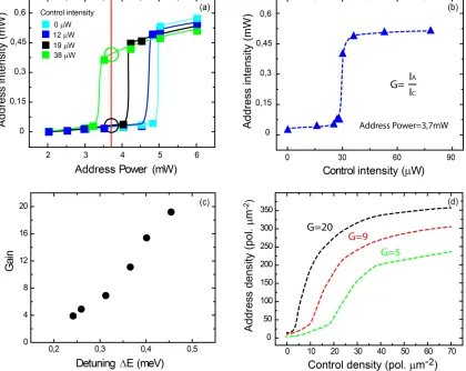
Transistor Operation. In Fig. 2a, the characteristic curves of the Address intensity are shown for
different values of . The threshold power lowers when increasing the control density, passing from
in the case of no control beam to in correspondence of a control intensity
of 38 W. Therefore, for a fixed value of , the Address can be switched on (green circle in Fig. 2a) and
off (black circle in Fig. 2a) by changing the polariton density in the Control state.
This operational principle is verified in Fig. 2b, where the Address intensity (blue triangles) is plotted as a
function of the Control intensity for , corresponding to the red line in Fig. 2a. The address
is switched on (off) for Control intensities above (below) the threshold of 30 . The extinction ratio
of the Address intensity below and above threshold is . The gain G is defined as the ratio
between the polariton density in the Address above threshold and the polariton density in the Control
state required for the switching operation, and it is directly obtained by measuring the emission
intensities of Address and Control at threshold, . Note that the gain is defined only by the
emission intensities, which are directly related to the number of polaritons inside the cavity. Indeed, the
gain requirement consists in the fact that few polaritons in the Control must be able to switch on
enough polaritons in the Address so that, moving in the plane they can act as a Control for the next
transistor in cascade. In this case, a gain is obtained, showing that the density of the Address is
more than one order of magnitude larger than the polariton density in the Control. This threshold
corresponds to a density between 5 and 20 polaritons/µm2 in the Control state, which means few
attojoule/µm2. Even considering the relatively wide laser spot used in these experiments to avoid any
reaching, at most, an energy of few femtojoule, figure which could be strongly reduced by, for instance,
designing ad hoc waveguides and mesa structures with lateral size down to a few micrometers.
An interesting point is that the value of the amplification at threshold can be modulated by tuning the
energy of the exciting laser, obtaining a higher gain when the detuning of the Address is increased,
[image:8.612.99.519.77.411.2]discriminator regime is wide enough to allow a modulation of the gain from 4 to 19 (note that, in order
to obtain a higher gain for larger detuning, the Address power has to be increased accordingly). The
polariton densities of Control and Address have been theoretically simulated and confirm the
experimental observation of a strong gain at threshold, which is triggered by a polariton density lower
than 10 polariton/µm2 in the Control state. These numbers can be improved even further with
microcavities of higher finesse and by reducing the Address detuning (though, in this case, with a
trade-off of a smaller gain). In Fig.2d, the simulations are run for three different powers of the Address beam
(0.70 , 0.76 and 0.83 , corresponding to the green, red and black color respectively), showing
that the control threshold can be lowered by tuning, for instance, the Address power.
Propagation and Cascadability. We are now interested in the possibility to demonstrate full
cascadability by triggering the absorption of a second Address beam, spatially separated from the first,
through the propagation of polaritons within the plane of the microcavity. This scheme, sketched in
Fig.3a-b, can be seen as two transistors in series in which the first input controls In
order to do so, the real and momentum space images of the emission intensities have been
simultaneously recorded for the whole area comprising the two transistors. As shown in Fig. 3, the
second Address beam (labelled B in Fig. 3) is focused at a distance of 40 µm from the first Address
(labelled A), both A and B being below threshold (Fig. 3c and Fig. 3d for real and momentum space
respectively). Note that the Control beam (labelled C) is spatially overlapping only with beam A and
having orthogonal momentum. In Fig. 3d, the 2D image of the momentum space shows that the
momenta of A, B and C in the microcavity plane point in different directions. When the density of C is
increased the switching of A results in a polariton fluid moving towards point B, bringing above
threshold the second Address B, which in turn propagates in the perpendicular direction. This is shown
in Fig. 3e and Fig. 3f, for real and momentum space respectively, with a color scale corresponding to 20
times higher intensity with respect to the off regime of Fig. 3c-d. When the Control density in the first
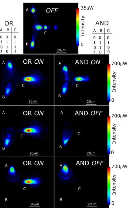
AND/OR gates. Interestingly, two or more Controls can contribute to the activation of the Address,
furnishing the basis for the operation of the transistor as a logic gate. We explore here the possibility to
use two propagating polariton fluids (labelled A and B in Fig.4) to control the output of a third transistor
(labelled C in Fig.4). A and B are separated by a distance of about 70 m, while C is placed near the
intersection point of A and B, as shown in Fig.4, and directed horizontally rightward. The transistor C is
[image:10.612.131.485.67.408.2]Fig.4), while it is working as an OR gate if A or B only are required for the activation of C (left column of
Fig.4). In Fig.4 the AND gate is obtained by lowering the Address power of C by 10% with respect to the
OR case[41]. The upper panel of Fig. 4 shows the OFF state, when both the control of A and B are below
threshold.
Fig. 4: Three transistors scheme (A,B and C, spatially separated by a distance of about 30 m) in which C acts as AND/OR logic gate with inputs A and B. When A, B and C are below threshold as in (a), their output
intensities are lower than 35 W. The interference pattern originated by the three fluids is visible near the intersection point in this low density regime. Due to the increase of the intensities above threshold, the color scales in panels (b,c,d,e,f,g) are reduced by a factor 20 as compared with panel (a). The OR gate is described in the left column with both A and B on (b), B only on (c), A only on (d). C is always activated
when A or B or both are on. The AND gate is obtained by lowering 10% the Address power of C, and it is
[image:11.612.197.418.192.550.2]Discussion
Optical amplification and switching can be obtained in strongly-coupled exciton-photon systems through
the peculiar non-linear properties of microcavity polaritons. The light-matter nature of these
quasi-particles allows to obtain switching times of the order of the cavity lifetime (10ps), with the additional
advantage of using ultra low activation energies (1 fJ). The results presented in this Article show that
using polariton states with finite velocities it is possible to realize an all-optical transistor which is based
on the propagation of polariton fluids the chip plane. The on-state propagates out of the injection region
towards a second injection point, being able to activate a new polariton fluid with different velocity and
direction. Even with the complication to guide polariton fluids in the planar (two-dimensional)
microcavity used in this experiment, we demonstrate that one transistor is able to trigger the on state of
another transistor spatially separated from the first. This operation takes place all inside the microcavity,
allowing for multiple interconnections to occur in the plane of the semiconductor chip. We have shown
the amplification properties of the transistor in Fig. 2, and proven the cascadability of the system in the
experiments of Fig. 3. Indeed, amplification and cascadability are both essential requirements for the
connectivity of more transistors in the same circuit. This is further proven in Fig. 4, where two outputs
are used as inputs into one transistor, enabling the AND/OR logic operation as a three terminal system
(two inputs and one output). Finally, looking at Fig. 2b, it can be observed that the on-state intensity of
the output is almost independent from the input intensity (above threshold). This allows the connection
of multiple inputs into the same gate, restoring the correct output level.
The results presented so far provide the basis for the integration of polariton systems in future
realization of all-optical circuits. In this context, further investigations on the hydrodynamic properties
of polaritons should be dedicated to the design of suited geometries for the division and coupling of
polariton fluids in guiding structures. In particular, the propagation properties and footprint can be
strongly improved using one-dimensional polariton wires etched in high-quality samples (Q > 20000).
Note that in this case the finite velocity of the polariton fluids can be controlled independently of the
angle of incidence of the injection laser, for example by providing an exciton-photon detuning with a
gradient in the desired direction [42] or by controlling the expansion of the polariton fluid [37]. In
addition to the classic gates, 0D pillar structures could be also used to exploit the energy quantisation
and other phenomena typical of localised superfluids such as the Josephson effects or the conditional
tunnelling. This device shows an interesting potential for future optical operation, which could take
References:
1. Paul, B.C., A. Agarwal, and K. Roy, Low-power design techniques for scaled technologies.
Integr. VLSI J., 2006. 39(2): p. 64-89.
2. Bohr, M.T., Nanotechnology goals and challenges for electronic applications.
Nanotechnology, IEEE Transactions on, 2002. 1: p. 56.
3. Wada, O., Femtosecond all-optical devices for ultrafast communication and signal processing. New Journal of Physics, 2004. 6: p. 183.
4. Glesk, I., et al., All-optical switching using nonlinear subwavelength Mach-Zehnder on silicon. Opt. Express, 2011. 19(15): p. 14031-14039.
5. Johnston, W.J., J.P. Prineas, and A.L. Smirl, Ultrafast all-optical polarization switching in Bragg-spaced quantum wells at 80 K. Journal of Applied Physics, 2007. 101(4): p. 046101-3. 6. Almeida, V.R., et al., All-optical control of light on a silicon chip. Nature, 2004. 431(7012):
p. 1081-1084.
7. Nozaki, T., et al., Sub-femtojoule all-optical switching using a photonic-crystal nanocavity.
Nat Photon, 2010. 4: p. 477.
8. Mori, T., Y. Yamayoshi, and H. Kawaguchi, Low-switching-energy and high-repetition-frequency all-optical flip-flop operations of a polarization bistable vertical-cavity surface-emitting laser. Applied Physics Letters, 2006. 88: p. 101102.
9. Hwang, J., et al., A single-molecule optical transistor. Nature, 2009. 460(7251): p. 76-80. 10. Miller, D.A.B., Are optical transistors the logical next step? Nat Photon, 2010. 4(1): p. 3-5. 11. De Giorgi, M., et al., Control and Ultrafast Dynamics of a Two-Fluid Polariton Switch.
Physical Review Letters, 2012. 109(26): p. 266407.
12. Savasta, S., O. Di Stefano, and R. Girlanda, Many-Body and Correlation Effects on Parametric Polariton Amplification in Semiconductor Microcavities. Physical Review Letters, 2003. 90(9): p. 096403.
13. Savvidis, P.G., et al., Angle-Resonant Stimulated Polariton Amplifier. Physical Review Letters, 2000. 84(7): p. 1547.
14. Huang, R., F. Tassone, and Y. Yamamoto, Experimental evidence of stimulated scattering of excitons into microcavity polaritons. Physical Review B, 2000. 61(12): p. R7854.
15. Ciuti, C., et al., Theory of the angle-resonant polariton amplifier. Physical Review B, 2000. 62(8): p. R4825.
16. Stevenson, R.M., et al., Continuous Wave Observation of Massive Polariton Redistribution by Stimulated Scattering in Semiconductor Microcavities. Physical Review Letters, 2000. 85(17): p. 3680.
17. Saba, M., et al., High-temperature ultrafast polariton parametric amplification in semiconductor microcavities. Nature, 2001. 414(6865): p. 731-735.
18. Baas, A., et al., Optical bistability in semiconductor microcavities. Physical Review A, 2004. 69(2): p. 023809.
19. Tredicucci, A., et al., Optical bistability of semiconductor microcavities in the strong-coupling regime. Physical Review A, 1996. 54(4): p. 3493.
20. Gippius, N.A. and et al., Nonlinear dynamics of polariton scattering in semiconductor microcavity: Bistability vs. stimulated scattering. EPL (Europhysics Letters), 2004. 67(6): p. 997.
21. Whittaker, D.M., Numerical modelling of the microcavity OPO. physica status solidi (c), 2005. 2(2): p. 733-737.
23. Bajoni, D., Optical bistability in a GaAs-based polariton diode. Phys. Rev. Lett., 2008. 101: p. 266402.
24. Paraïso, T.K., et al., Multistability of a coherent spin ensemble in a semiconductor microcavity. Nat Mater, 2010. 9(8): p. 655-660.
25. Amo, A., et al., Exciton-polariton spin switches. Nat Photon, 2010. 4(6): p. 361-366. 26. Kasprzak, J., et al., Bose-Einstein condensation of exciton polaritons. Nature, 2006.
443(7110): p. 409-414.
27. Balili, R., et al., Bose-Einstein Condensation of Microcavity Polaritons in a Trap. Science, 2007. 316(5827): p. 1007-1010.
28. Amo, A., Collective fluid dynamics of a polariton condensate in a semiconductor microcavity. Nature, 2009. 457: p. 291-295.
29. Amo, A., Superfluidity of polaritons in semiconductor microcavities. Nature Phys., 2009. 5: p. 805-810.
30. Sanvitto, D., et al., Persistent currents and quantized vortices in a polariton superfluid. Nat Phys, 2010. 6(7): p. 527-533.
31. Amo, A., et al., Polariton superfluids reveal quantum hydrodynamic solitons. Science, 2011. 332(6034): p. 1167-1170.
32. Sanvitto, D., et al., All-optical control of the quantum flow of a polariton condensate. Nat Photon, 2011. 5(10): p. 610-614.
33. Christopoulos, S., et al., Room-Temperature Polariton Lasing in Semiconductor Microcavities. Physical Review Letters, 2007. 98(12): p. 126405.
34. Liew, T.C.H., A.V. Kavokin, and I.A. Shelykh, Optical circuits based on polariton neurons in semiconductor microcavities. Phys. Rev. Lett., 2008. 101: p. 016402.
35. Shelykh, I.A., et al., Proposal for a Mesoscopic Optical Berry-Phase Interferometer. Physical Review Letters, 2009. 102(4): p. 046407.
36. Liew, T.C.H., et al., Exciton-polariton integrated circuits. Physical Review B, 2010. 82(3): p. 033302.
37. Wertz, E., et al., Spontaneous formation and optical manipulation of extended polariton condensates. Nat Phys, 2010. 6(11): p. 860-864.
38. Johne, R., et al., Polaritonic analogue of Datta and Das spin transistor. Physical Review B, 2010. 81(12): p. 125327.
39. Gibbs, H.M., Optical Bistability: Controlling Light with Light1985.
40. Cancellieri, E., et al., Multistability of a two-component exciton-polariton fluid. Physical Review B, 2011. 83(21): p. 214507.
41. Note:, In this way we are slightly reducing the gain in the AND gate. Due to the nonlinear behaviour of the transistor, the difference is only of about 10% of the Address power and it
e > 10 even for the
AND gate.
Methods
Two-component Gross-Pitaevskii equation. A standard way to model the dynamics of the system of
resonantly-driven polaritons in a planar microcavity is to use a Gross-Pitaevskii equation for coupled
cavity and exciton field ( and ) generalized to include the effects of the resonant pumping and
decay :
(1)
where the single particle polariton Hamiltonian H0 reads:
Where is the cavity dispersion as a function of the in-plane wave vector and
where the photon mass is and is the bare electron mass. For these
simulations a flat exciton dispersion relation will be assumed and the case of zero
detuning at normal incidence considered. The parameters , and are the
Rabi frequency and the excitonic and photonic decay rates respectively and are taken close to
experimental values: , , and . In this model polaritons
are injected into the cavity in two states (address and control) by two coherent and monochromatic
laser fields. The two laser fields share the same smoothen top-hat spatial profile with intensities
and for the address and the control respectively, and with full width at half maximum equal to 60
m. The two laser fields share also the same frequency but have different in-plane momentum
and . The exciton-exciton interaction strength is set to one by
rescaling both the cavity and excitonic fields and the pump intensities. Our theoretical results come
from the numerical solution of equation (1) over a two-dimensional grid (256x256) in a 140x140
box using a fifth-order adaptive-step Runge-Kutta algorithm. All the analyzed quantities are taken
the control state at thresholds results to be 3, 5 and 7 polaritons/ for the black, red and green
curve in Fig. 4d, respectively.
Evaluation of the polariton densities. For a measured address emission I = 0.5 mW, we obtain a
density , which corresponds to . The total address energy is
, which gives . Correspondingly, the control density is of about ,
which yields . In the calculation, we have used as the
polariton lifetime (extracted from the polariton linewidth), while is the polariton
energy and is the spot area (radius of . An upper limit can be alternatively obtained from
the exciting powers: considering the measured reflection of the address beam from the sample
surface (50%), the power of the address is 1.85 mW, and we obtain a density
, which corresponds to . The total address energy is thus .
Correspondingly, the control density is of about , which yields
.
Aknowledgements
We would like to thank A. Bramanti, V. Scarpa and C. Tejedor for useful discussions, P. Cazzato for
the technical assistance with the experiments, and F. M. Marchetti and M. H. Szymanska for the
development of the simulation code. This work has been partially funded by the FIRB Italnanonet
![Crystal structure of bis[2 (1H benzimidazol 2 yl) 4 bromophenolato κ2N3,O]cobalt(II)](data:image/gif;base64,R0lGODlhAQABAIAAAP///wAAACH5BAEAAAAALAAAAAABAAEAAAICRAEAOw==)