ENERGY SCAVENGING FOR MOBILE AND WIRELESS DEVICES USING CMOS RECTIFIER CIRCUIT
TAN CHONG WEI
This Report Is Submitted In Partial Fulfilment of Requirements For The Bachelor Degree of Electronic Engineering (Telecommunication Electronic) with Honours
Faculty of Electronics and Computer Engineering Universiti Teknikal Malaysia Melaka
v
vi
ACNOWLEDGEMENT
First and foremost, I would like to thanks all the lectures in University Teknikal Malaysia Melaka and Faculty of Electronic and Computer Engineering who have teach, instruct, train and educate me. Without them, I would never accomplish this work.
I would like to express my deepest gratitude to my project supervisor Dr Wong Yan Chiew for her generous guidance. Dr Wong is kind and responsible that she has always ensured my progress is done correctly. With her advice and help, the project could conduct successfully. Beside I would also like to thank Dr Wong for giving me an opportunity to conduct this project. Through this project, I have enhanced my knowledge and experience.
Special thanks to Miss Bee Shei Er and Mr. Chan Lisen. They have spent time with me to discuss about the energy scavenging system topics. They are willing to share their knowledge on related topic. I am much appreciated with the good relationship with them and all the collaboration has been built up.
Besides, another thank I would like to give to them who have evaluate my work. I appreciate all the suggestion they have provided. Moreover, I would like to thanks Mr Sreedharan Baskara Dass who has provided a technical support on my project. In addition, I would like to thank my classmate who has helped me directly and indirectly.
vii
ABSTRACT
viii
ABSTRAK
ix
TABLE OF CONTENTS
CHAPTER CONTENT PAGE NUMBER
PROJECT TITLE i
CONFIRMATION ON REPORT STATUS ii
DECLARATION iii
SUPERVISOR'S CONFIRMATION iv
DEDICATION v
ACNOWLEDGEMENT vi
ABSTRACT vii
ABSTRAK viii
TABLE OF CONTENT ix
LIST OF FIGURE xii
LIST OF TABLE xiv
LIST OF ABBREVATIONS xv
I INTRODUCTION
1.1. PROJECT OVERVIEW 1
1.2. PROBLEM STATEMENT 2
1.3. OBJECTIVE 3
1.4. SCOPE OF PROJECT 3
1.5. PROJECT DEVELOPMENT 3
1.6. REPORT OUTLINE 4
II LITERATURE REVIEW
2.1. OVERVIEW 6
2.2. RF ENERGY SCAVENGING 6
x
2.4. VOLTAGE MULTIPLIER 9
2.5. POWER CONVERSION EFFICIENCY (PCE) 9 2.6. METAL-OXIDE-SILICON FIELD-EFFECT
TRANSISTORS (MOSFETS)
10
2.6.1 MOSFET Structure 10
2.6.2 Threshold Voltage 11
2.6.3 I-V Characteristics 12
2.6.4 Body Effect 13
2.7. THRESHOLD VOLTAGE CANCELLATION 13 2.7.1 Bulk modulation technique 14 2.7.2 Cross Coupled Rectifier 16 2.7.3 Control circuit based and comparator based rectifier 20
2.8. SUMMARY 24
III METHODOLOGY
3.1. OVERVIEW 25
3.2. SPECIFICATION SETTING 26
3.3. SCHEMATIC DESIGN 26
3.3.1 Simulation Setting 27
3.4. LAYOUT DESIGN 29
3.4.1 Physical Verification Setting 29
3.5. SUMMARY 30
IV RECTIFIER ARCHITECTURE
4.1. OVERVIEW 31
4.2. RECTIFIER ARCHITECTURE 31
4.3. SUPPORTING CIRCUIT 35
4.4. SUMMARY 36
xi
5.1. OVERVIEW 37
5.2. MATCHING CIRCUIT 37
5.3. PMOS & NMOS PARAMETRIC STUDY 40 5.4. LOAD RESISTOR PARAMETRIC STUDY 42
5.5. SUMMARY 43
VI RESULT AND ANALYSIS
6.1. OVERVIEW 44
6.2. TRANSIENT RESPONSE 44
6.3. LOAD CURRENT ANALYSIS 47
6.4. STEADY STATE OUTPUT VOLTAGE AND CURRENT 50 6.5. POWER CONVERSION EFFICIENCY AND VOLTAGE
GAIN
52
6.6. LAYOUT DESIGN 53
6.7. SUMMARY 57
VII CONCLUSION AND RECOMMENDATION
7.1. OVERVIEW 58
7.2. PROJECT SUMMARY 58
7.3. FUTURE WORK RECOMMENDATION 59
BIBLIOGRAPHY 60
xii
LIST OF FIGURE
Figure 2.1 RF energy scavenging system ... 7
Figure 2.2 (a) Half wave rectifier (b) Full wave rectifier ... 8
Figure 2.3 Voltage multiplier ... 9
Figure 2.4 Structure of n-type MOS device ... 10
Figure 2.5 Substrate connection of n-type MOS device ... 11
Figure 2.6 Bulk modulation arrangement ... 14
Figure 2.7 (a) Bulk Modulation PMOS arrangement based rectifier (b) Conventional PMOS arrangement based rectifier... 15
Figure 2.8 (a) Bulk Modulation implemented Self Vth cancellation scheme (b) Conventional rectifier implemented Self Vth cancellation scheme ... 15
Figure 2.9 Voltage Multiplier using Bulk Modulation PMOS ... 16
Figure 2.10 Cross coupled rectifier ... 17
Figure 2.11 Cross-coupled rectifier with matching ... 18
Figure 2.12 ( a) Cross-coupled voltage multiplier (b) Conventional voltage multiplier ... 18
Figure 2.13 Cross coupled rectifier with modified PMOS transistor ... 19
Figure 2.14 Rectifier with Vth compensation technique ... 21
Figure 2.15 Rectifier with an internal VTH cancellation method ... 22
Figure 2.16 Rectifier and comparator ... 23
Figure 2.17 Comparator of rectifier ... 23
Figure 3.1 Project flow chart ... 25
Figure 3.2 Simple simulation setting in Cadence Virtuoso ... 27
Figure 3.3 Transient response ... 27
Figure 3.4 S-parameter analysis ... 28
Figure 3.5 Periodic steady state analysis ... 28
Figure 3.6 DRC setting in Calibre ... 29
Figure 3.7 LVS setting in Calibre ... 30
xiii
Figure 4.1 Proposed cross-coupled rectifier ... 32
Figure 4.2 Cascaded cross coupled rectifier ... 34
Figure 4.3 Supporting circuit for rectifier ... 35
Figure 5.1 Return loss parametric analysis ... 38
Figure 5.2 Matched S11 return loss ... 39
Figure 5.3 Matched input impedance (a) real-Z11 (b) imaginary-Z11 ... 40
Figure 5.4 Transistor size parametric analysis (a) NMOS (b) PMOS ... 41
Figure 5.5 Load resistor parametric analysis ... 42
Figure 6.1 Transient response in 1-cascaded stage (a) output voltage (b) output current ... 45
Figure 6.2 Transient response in 3-cascaded stages (a) output voltage (b) output current . 45 Figure 6.3 Transient response in 5-cascaded stage (a) output voltage (b) output current ... 46
Figure 6.4 Load capability at -20dBm (a) 1µA (b) 10µA (c) 100µA ... 47
Figure 6.5 Load capability at -10dBm (a) 1µA (b) 10µA (c) 100µA ... 48
Figure 6.6 Load capability at 0dBm (a) 1µA (b) 10µA (c) 100µA ... 49
Figure 6.7 Load capability at 10dBm (a) 1µA (b) 10µA (c) 100µA ... 50
Figure 6.8 Output voltage versus input power ... 51
Figure 6.9 Output current versus input power ... 51
Figure 6.10 PCE versus input power ... 52
Figure 6.11 Voltage gain versus input power ... 53
Figure 6.12 Transistor model layout (a)pm_hprf (b)nm_hprf ... 54
Figure 6.13 fm3m1rf metal finger capacitor model layout ... 54
Figure 6.14 Rectifier layout ... 55
Figure 6.15 DRC check report ... 55
Figure 6.16 LVS test report ... 56
xiv
LIST OF TABLE
Table 2.1 Bulk Modulation topologies comparison ... 16
Table 2.2 Cross coupler rectifier comparison ... 20
Table 2.3 control circuit based and comparator based rectifier ... 24
Table 3.1 Rectifier specification ... 26
xv
LIST OF ABBREVATIONS
RF - Radio Frequency AC - Alternative Current DC - Direct Current IC - Integrated Circuit LDO - Low-dropout regulator
CMOS - Complementary Metal-Oxide Semiconductor MOSFET - Metal–oxide–semiconductor Field-effect Transistor NMOS - N-type MOSFET
PMOS - P-type MOSFET DRC - Design Rule Check LVS - Layout Versus Schematic PEX - Parasitic Extraction
PCE - Power Conversion Efficiency SVC - Self Vth Cancellation
DTMOS - Dynamic Threshold-voltage MOSFET LAN - Local Area Network
1
CHAPTER 1
INTRODUCTION
1.1. Project Overview
RF energy has become one of the very common man-made energy source due to the highly usage of radio sources device such as mobile phones, television, WIFI devices etc. At the same time, the demand for battery free application like wireless sensor-based network is growing up. Compared to a self-powered system, a battery’s life span is limited to a system. This could be a challenge to achieve the fast grows in the integrated circuit technology as described by Moore’s law. Therefore, RF energy harvesting has become dominant to substitute a battery as the RF energy source is cheap and easy available. RF energy can be harvest with energy scavenging circuit. The circuit could extract the electrical energy from the ambient RF energy source and convert it into a stable DC voltage. One of the important blocks in the RF energy harvesting circuit is the rectifier circuit.
2
In this project, a CMOS rectifier will be implemented from schematic entry to simulation and the layout drawing with verification. The design of the rectifier will focus on the threshold cancellation and power conversion efficiency of the CMOS rectifier.
1.2. Problem Statement
As the emerging of Internet of things in the future, there will be billions of sensors, mobile devices and wireless devices would be needed to power up. However to power up those devices with battery is impractical. Therefore a RF energy scavenging system can be used as substitution for battery and provide power to the mobile and wireless devices. A CMOS rectifier is one of the important parts in the RF energy scavenging system which convert RF energy to stable DC supply.
To design a CMOS rectifier, the power conversion efficiency is the main consideration. The factor that affects the efficiency of the rectifier is the threshold voltage of diode. The RF energy that received by an antenna from the surrounding could only achieved in a low voltage. High threshold voltage cause major voltage drop, hence achieve low power conversion efficiency. The case can be even worse, if the rectifier is cascaded in multiple stage, the total threshold voltage drop could be higher. Zero Vth MOS or Schottky diode which have low threshold could use to solve the problem. However, Zero Vth MOS could result in high reverse leakage current while Schottky diodes are not supported in all CMOS technologies. Therefore a threshold cancellation technique needs to be proposed.
3
1.3. Objective
The objectives of this project are:
To identify the key parameters in CMOS rectifier
To design a CMOS rectifier circuit with low threshold voltage
To improve the power conversion efficiency of CMOS rectifier that could be applied on the RF harvesting circuit
To verify the proposed methodology theoretically and analytically through modelling
1.4. Scope of Project
In this project, the CMOS rectifier would be done in 130nm CMOS technology. Schematic and layout of the CMOS rectifier would be designed and simulated in the Synopsys IC design software. The input signal for the CMOS rectifier would be 2.45GHz. It would able to be operating at input power as low as -20dBm. The input RF signal will be converted into higher DC voltage. The threshold voltage of the CMOS rectifier would be eliminated effectively and the CMOS rectifier would have better improvement on the power conversion efficiency as compared to conventional rectifier. In the end the output voltage rectifier should achieve a level that may be filtered by regulator in the energy scavenging system and finally usable for mobile and wireless devices.
1.5. Project Development
4
1.6. Report Outline
Five chapters are written in this thesis. The information gathered from the research and investigation is presented in this thesis. Each description and detail for each chapter is explains below:
Chapter 1 – Introduction
This is the most important part in this thesis. In this chapter, general ideal of the CMOS rectifier design have been descripted. The aims of the project have been stated and the boundaries of this work have been discussed.
Chapter 2 – Literature Review
In this chapter, a generic knowledge of CMOS rectifier design and previous research of CMOS rectifier have been studied. The generic knowledge includes the conceptual framework and applies theory of CMOS rectifier. The conceptual framework is such as brief concept of RF energy scavenging. While applies theory are such as rectifier, voltage multiplier, power convention efficiency and characteristic of MOSFET. Besides, the previous researches on CMOS rectifier are focus on the threshold cancellation technique. The specification and validity of previous researches are discussed. The previous researches that have studied can be categories into three parts which are Bulk Modulation Technique, Cross Coupler Rectifier and Comparator Based & Control Circuit Based Rectifier.
Chapter 3 – Methodology
This chapter will provides detailed method and procedures of designing the CMOS rectifier. A flow chart of the CMOS rectifier design and development is shown. The design specifications are stated precisely in this chapter. The steps involved in the CMOS rectifier design include schematic design, design simulation, layout design, layout validation and post-simulation.
Chapter 4 – Rectifier Architecture
cross-5
coupled rectifier is introduced in this chapter too. Next, the supporting circuit for the rectifier is explained block by block. The blocks which included in the supporting circuit are the RF port, balun, L-matching circuit, rectifier and the output port.
Chapter 5 – Design Parameters
There is several parameter need to be defined in order to maximize the performance of the rectifier. In this chapter, the value of the capacitor and inductor in L-matching circuit is determined by s-parameter analysis. Next, the width and length of PMOS and NMOS are identified by parametric study. Beside, another parametric study is carried for load resistor.
Chapter 6 – Result and Analysis
This chapter is one of the important parts of this thesis. It describes the performance of the rectifier. The analysis that have been performed in this chapter including the transient response, load current analysis, steady state output voltage and current, power conversion efficiency and voltage gain. The transient response shows the output achieved at a stable DC. The load current analysis is to test the load capability of the transistor. Moreover, the steady state output voltage and current shows the maximum output voltage and the output current that the rectifier could achieve. In addition, the power conversion efficiency and voltage gain represent how much power the rectifier can conserve and how sensitive the rectifier could receive input power.
Chapter 7 – Conclusion and Recommendation
6
CHAPTER 2
LITERATURE REVIEW
2.1. Overview
This chapter includes the background theory to design a CMOS rectifier. First of all, a brief concept of RF Energy Scavenging is introduced. Next the basic concept of rectifier, voltage multiplier and power conversion efficiency are discussed. Furthermore, the generic concepts of MOSFET such as MOSFET structure, threshold voltage, I-V characteristics and body effect have been review. Besides, the previous researches of CMOS rectifier have been studied. These researches are focus on the threshold voltage cancelation technique such as Bulk modulation technique, cross-coupler rectifier and Comparator Based & Control Circuit Based Rectifier. Their specifications, operation, background theory and findings are described. Results of several topologies are compared.
2.2. RF Energy Scavenging
7
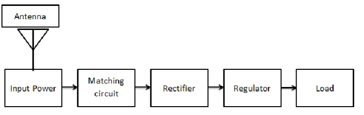
Figure 2.1 RF energy scavenging system
The antenna is use to receive the RF energy from the surrounding. The received RF energy is usually low. It could even lower if RF energy is received by a small gain antenna which is commonly used by mobile device. The received RF energy becomes the input power for the rectifier. Before the rectifier, a matching circuit is used to decrease the reflected power from the source into the rectifier circuit and this could prevent energy loss in the circuit. Next, the function of the rectifier circuit is to convert the RF input signal into stable DC signal. A regulator is use to provide a smooth and stable linear DC signal. A Low-dropout regulator (LDO) can be a suitable component in this part. LDO could regulate the output voltage to a useful level in order to address the power needs for applications. Lastly, the regulator connected to the load of related application, the destination where the power wants to deliver.
2.3. Rectifier
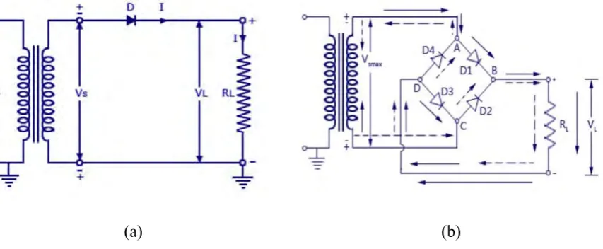
A rectifier is use to convert a signal from ac to dc, or usually convert a zero average value signal into a nonzero average signal. Diode is usually used to construct rectifier such as half-wave rectifier and full-wave rectifier. To receive low power RF energy, a Schottky Diode with low forward voltage drop can be used to perform RF-DC conversion. N-MOSFET and P-N-MOSFET can used to replace diode, especially the Schottky diode do not be supported in CMOS technology
8
(a) (b)
Figure 2.2 (a) Half wave rectifier (b) Full wave rectifier
There are only 1 diode will be use to design a half- wave rectifier while full wave rectifier require 4 diodes. The only diode of half wave rectifier will turn ‘on’ during positive half cycle of signal and turn ‘off’ during the other cycle. For full wave rectifier, during any half cycle of the signal, two diodes will be turn ‘on’ while the other two will be turn ‘off’.
In fact, there would be a forward voltage or threshold voltage drop for every forward bias diode. This would cause a major drop on dc level. It will perform very bad power convention efficiency especially for a low input power. Besides, the power convention efficiency is affected by the reverse leakage current too. High reverse leakage current means a high power lost.
There are two main reasons that cause the undesired reverse leakage current. Reverse leakage current occur most the time when the diode or MOSFET do not turn ‘off’ fast enough, current will flow in opposite direction during the transition of the state. Another reason that causes the reverse leakage current is the low threshold voltage of diode or MOSFET. Because of threshold voltage, it could efficiently block the current during the reverse bias. That is the reason for zero-Vth diode is not suitable to be used in the design of rectifier. However, as mention before high threshold voltage decrease the power conversion efficiency of the rectifier.
[image:23.595.95.522.71.247.2]9
2.4. Voltage multiplier
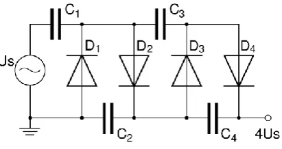
[image:24.595.204.410.193.302.2]Voltage multiplier is similar to the rectifier but it could convert the AC from low voltage to higher DC voltage. The voltage multiplier circuit consists of two important components, capacitor and diode. Figure 2.3 shows a simple construction of a voltage multiplier.
Figure 2.3 Voltage multiplier
The capacitors are act as energy-storage element while the diode is use to control the connection of voltage to the capacitor. In the first cycle of the signal, a capacitor C1 is connected to the supply would charge to that same voltage. In the second cycle, C2 will be charge to double of supply voltage. So as next following cycle, C3 and C4 will be charge to double of supply voltage too. The sum of voltages under C2 and C4 rise to 4 times of supply voltage. The voltage can be further increased by adding more capacitor and diode.
2.5. Power Conversion Efficiency (PCE)
Power conversion efficiency or PCE is a measure of the performance of a power conversion circuit such as RF to DC conversion. High PCE represent low power loss in the system. There are several reasons that could the power loss, such as thermal loss, mismatch load and leakage current. The PCE could be calculated as the ratio of delivered power to the load and the input power. The PCE, 𝜂is given that equation (2.1)
𝜂 = 𝑃𝑙𝑜𝑎𝑑
𝑃𝑖𝑛 (2.1)