COMMUNICA
TION
Grain Boundary Controlled Electron Mobility
in Polycrystalline Titanium Dioxide
Suzanne K. Wallace and Keith P. McKenna *
S. K. Wallace, Dr. K. P. McKenna Department of Physics University of York
Heslington, York YO10 5DD United Kingdom
E-mail: [email protected]
DOI: 10.1002/admi.201400078
devices has been proposed as essential to the switching mecha-nism. [ 5 ] Despite its importance for these numerous applications
defi nitive information on the electron trapping properties of grain boundaries in TiO 2 is still lacking.
First principles theoretical calculations can be invaluable to provide insight into electron trapping effects in oxide mate-rials. [ 11–13 ] Many theoretical investigations performed within
the framework of density functional theory (DFT) have studied electron trapping in TiO 2 , including bulk crystals (both rutile
and anatase polymorphs), surfaces and point defects. [ 11,12,14 ]
These calculations are extremely challenging but accurate pre-diction of electron trapping can be achieved using methods such as hybrid-DFT and DFT+U which correct the self-interac-tion (SI) error which can lead to artifi cial electron delocalizaself-interac-tion (e.g. see ref. [ 15 ] ). For example, it has been shown that electrons can become self-trapped at Ti ions in the rutile crystal forming small polarons consistent with experimental evidence. [ 12,16 ] At
surfaces and near oxygen vacancies multiple confi gurations of trapped electrons can have similar stability and dynamic hopping between sites has been predicted. [ 17 ] On the other
hand, electron trapping in the anatase crystal is much weaker explaining its much higher electron mobility. Surprisingly there have been no studies of electron trapping near intrinsic inter-facial defects such as grain boundaries which are always pre-sent in nanocrystalline TiO 2 . Here, we combine fi rst principles
based modeling with a kinetic Monte Carlo (KMC) simulation in order to investigate the effect of grain boundaries on elec-tron trapping and mobility. We consider a model Σ5 (210)[001] tilt grain boundary in rutile [ 18 ] and focus on the intrinsic
elec-tron trapping properties of the grain boundary without defects or impurities which is something that is very diffi cult to do experimentally.
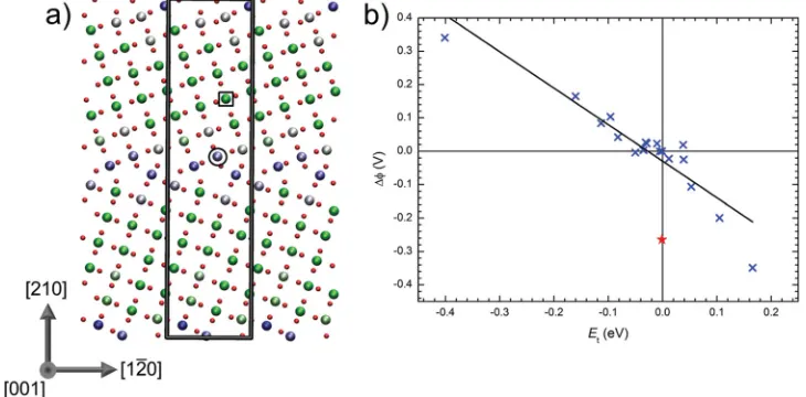
Grain-boundary models have been obtained through a sys-tematic screening of different atomic confi gurations using a classical interatomic potential approach [ 19 ] followed by refi
ne-ment at the DFT level. DFT calculations are performed within the DFT+U formalism which corrects the SI error suffi ciently to allow electron localization to be described while remaining com-putationally feasible for complex systems containing more than 300 atoms (full details of these calculations are available in the Methods section and Supporting Information). Figure 1 a shows the predicted structure of the Σ5 (210)[001] tilt grain boundary in rutile which is consistent with previous transmission electron microscopy studies [ 18 ] and DFT calculations. [ 20 ] The structure
exhibits a high degree of order with only a few undercoordinated Ti and O ions close to the grain boundary plane. The electrostatic potential also varies signifi cantly near the grain boundary which can play an important role in stabilizing trapped electrons. For example, the electrostatic potential on Ti ions within 5 Å of the The trapping and mobility of electrons in nanocrystalline oxide
materials underpins a diverse range of applications in areas such as solar energy generation, catalysis, gas sensing and nanoelectronics. [ 1–5 ] Grain boundaries, one of the most
perva-sive defects in these materials, are widely believed to be critical in controlling electron mobility but probing their effects directly has proved extremely challenging. Here, we provide atomistic insight into this important issue through fi rst principles based modeling of the interaction of electrons with grain boundaries in TiO 2 . We show that perturbations in electrostatic potential
are responsible for high concentrations of strong electron trap-ping sites at grain boundaries which hamper electron transport between grains. However, this effect is partially ameliorated at high current densities (>0.01 mAcm −2 ) as a result of a highly
nonlinear trap fi lling effect pointing to ways to help improve the performance of materials for applications such as dye-sensi-tized solar cells and photocatalysts. [ 1–6 ]
Nanocrystalline oxides, encompassing both porous powders and dense ceramic materials, are a ubiquitous form of techno-logical material. However, TiO 2 is perhaps exceptional in the
incredibly wide range of applications it fi nds, including photo-catalysts for self-cleaning glass and water splitting, [ 3 ]
dye-sensi-tized solar cells (DSSCs) for solar energy generation, [ 1–6 ] Li-ion
battery materials for energy storage [ 7 ] and resistive switching
memories for low power and non-volatile data storage. [ 5 ] Key to
the performance of these varied applications is the transport of electrons which may be introduced by optical excitation, elec-trical injection or doping. For example, in catalytic applications the polaronic trapping of electrons at TiO 2 surfaces produces
highly reactive Ti 3+ sites which can facilitate chemical reactions.
In DSSCs, electrons injected into the nanocrystalline network from photo-excited dye molecules must percolate through the TiO 2 network in order for electrons to reach the charge
collec-tion electrode. It has been suggested that interfaces between nanocrystals may present deep electron traps hindering elec-tron diffusion. [ 1,8–10 ] On the other hand, enhanced electron
diffusion along extended defects in resistive switching memory
COMMUNICA
TION
grain boundary varies between ±0.35 V of the bulk potential. While the boundary considered here represents a specifi c case it shares common features that are observed in more general grain boundaries in a range of materials, namely undercoordination, topological disruption and strain. [ 21–23 ]
To investigate the interaction of electrons with the grain boundary defect we attempted to localize an electron polaron at all inequivalent Ti sites within 1 nm of the grain boundary plane. This involved creating a precursor potential well for electron trapping by displacing nearest neighbor anions away from a particular Ti site by 0.1 Å followed by full self-consistent optimization of the structure. Bader charge analysis of the opti-mized structures indicates that about 0.4 electrons localize on a single Ti ion with the remaining charge distributed over neigh-bouring ions. [ 24 ] Far away from the grain boundary plane the
total energy is nearly independent of the site on which the elec-tron is trapped corresponding to a bulk-like elecelec-tron polaron. Therefore, in the following electron trapping energies, E t , are defi ned relative to the bulk-like electron polaron which we take as the site which is equidistant between the two grain boundary planes (indicated by the black square in Figure 1 a). We fi nd there is a strong correlation between the calculated trapping energy and the difference in on-site electrostatic potential with respect to the bulk (Figure 1 b). The almost linear correlation is found for all sites except one (indicated by the black circle in Figure 1 a) which is considerably more stable than should be expected given its electrostatic potential. This discrepancy can be understood because it is coordinated to two undercoordi-nated oxygen atoms. The greater freedom for ion distortion this affords on electron trapping stabilizes the polaron despite the low electrostatic potential. A linear fi t to the remaining points yields a slope of −1.1 ± 0.1, close to unity as would be predicted from a simple electrostatic model.
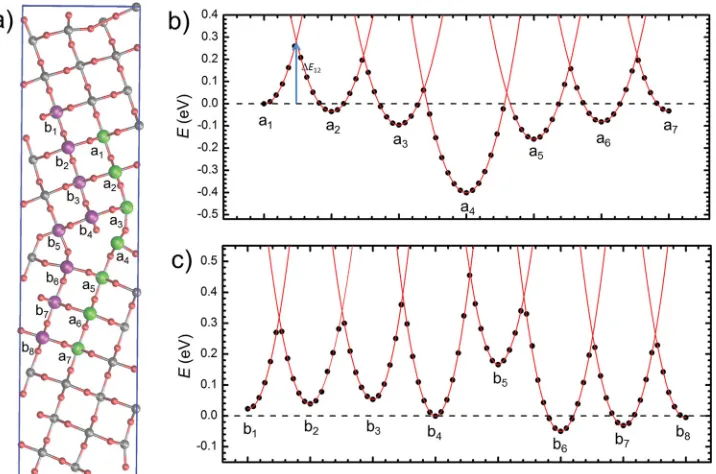
On the basis on the calculated trapping energies two pro-spective electron diffusion paths perpendicular to the grain
boundary are identifi ed labeled a and b in Figure 2 a. We con-sider electron transfer between nearest neighbor Ti sites ([001] direction in the bulk) which has been shown to be the domi-nant diffusion mechanism in the bulk crystal. [ 12 ] The diabatic
activation energies ( ΔE ij ) for electron hopping between adjacent sites are estimated by linearly interpolating the between the two optimized polaron geometries to obtain potential energy surfaces corresponding to an electron localized on either of the two sites (Figure 2 b). In the bulk-like region far from the grain boundary we fi nd the diabatic barrier to electron hopping ΔE bulk
is about 0.3 eV consistent with previous bulk calculations. [ 12 ]
Both paths a and b involve higher activation energies than in the bulk crystal therefore electron mobility will be reduced for electron transfer across the grain boundary. Parallel to the grain boundary we fi nd barriers are increased for transport in the [120] direction but slightly decreased for transport in the [001] direction. In all cases the potential energy surfaces can be described to a good approximation as parabolas which are verti-cally displaced according to the site's trapping energy resulting in the following Marcus-like model for the activation energy between two sites with trapping energies E i and E j
4
4 .
bulk 2
bulk
E E E E
E ij
j i
(
)
Δ =⎡⎣ − + Δ ⎤⎦
Δ (1)
To fully assess the effect of the grain boundary on mobility we simulate the correlated electron transport of a fl ux of elec-trons across a bicrystal using a KMC approach similar to that used in previous studies of electron transport in nanocrystalline TiO 2 and hematite. [ 7,25 ] The rate of electron hopping between
sites is described using the formalism of Marcus, Emin, Hol-stein, Austin and Mott [ 26 ] which gives the electron transfer rate
[image:2.594.113.478.73.253.2]in terms of the diabatic activation energies calculated above and the electronic coupling matrix elements H ab (see Sup-porting Information for details). Two crystals of approximate Figure 1. Predicted atomic structure of the Σ5 (210)[001] grain boundary in rutile. a) Periodic supercell (gray outline) containing two grain boundaries (one in the center of the image and one bridging the upper and lower edges). Additional periodic images of the supercell are shown in the fi gure to aid visualization. Large spheres represent Ti ions colored according to the magnitude of the on-site electrostatic potential (low=green, high=blue). Small red spheres represent oxygen ions. b) Correlation between the difference in on-site electrostatic potential with respect to the bulk (Δφ) and the electron trapping energy ( E t ). An almost linear correlation is found for all sites except one (red star) which is considerably more stable than should
COMMUNICA
TION
dimensions 21 × 20 × 50 Å are adjoined forming a (210)[001] grain boundary in the center as shown in in Figure 3 . Periodic boundary conditions are employed in the directions parallel to the grain boundary and electrons are injected from the left side with a fi xed rate (e.g. corresponding to photogenerated electron current). The probability for electrons to jump to unoccupied adjacent sites (in all directions) is calculated and electrons are removed from the simulation once they reach the right boundary. For calculation of the electron transfer rates we con-sider an adiabatic approximation (i.e. κ =el 1) and take an fre-quency characteristic of the longitudinal optical phonon mode in rutile for ν (24 THz). The trapping energy of an electron at
a given site is taken from the fi rst principles results described above. This energy is modifi ed by an electron-electron inter-action term which depends on the locations of electrons on nearby sites. The functional form was obtained from a numer-ical fi t to electron-electron interaction energies calculated in the bulk crystal using DFT+U. Consistent with the high dielectric constant of TiO 2 we fi nd a highly screened Coulomb interaction
which is essentially negligible beyond third nearest neighbor Ti sites. Calculation of H ab is more challenging since in general it requires simultaneously accurate elimination of self-interaction error and description of the TiO 2 band gap. In the following we
employ H ab = 0.2 eV for nearest neighbor hopping which is a value obtained in a previous study of electron transfer in bulk rutile. [ 12 ]
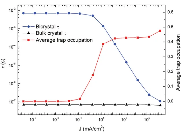
A series of KMC simulations are performed at room tem-perature with different electron injection rates corresponding to different current densities. After an initial transient period the system reaches a steady state where the time average of the number of electrons in the bicrystal and the net particle cur-rent is constant. To characterize the effi ciency of the electron transport we calculate the electron transit time (τ) which is the average time taken for an electron to travel across the bicrystal as a function of the current density. Figure 4 shows τ calculated for both the bicrystal cell and for a cell of equivalent crystal-lographic orientation but without a grain boundary (i.e. a bulk crystal) for reference. For current densities less than about 10 −2 mAcm −2 the electron transit time in the presence of a
single grain boundary is 7.0 ms at room temperature. This can be compared to the transit time for an equivalent distance in the bulk crystal which is 71 ns, fi ve orders of magnitude faster. The long transit time is a result of electrons trapping at Ti sites at the grain boundary (i.e. sites a 4 and equivalent) where they face
Figure 2. Potential energy surfaces for electron hopping in the vicinity of the Σ5 (210)[001] grain boundary in rutile TiO 2 . a) Two possible electron
dif-fusion paths ( a and b ) perpendicular to the grain boundary plane. b) Diabatic potential energy surfaces for electron hopping between Ti sites in path a . The points represent calculated energies while the lines are parabolas which have been fi t to the calculated points nearest to the local energy minima. c) Corresponding diabatic potential energy surfaces for electron hopping between Ti sites in path b .
Figure 3. Overview of the kinetic Monte Carlo simulation for modeling electron transport in a TiO 2 bicrystal. Three types of process are
[image:3.594.123.481.70.307.2] [image:3.594.53.292.515.653.2]COMMUNICA
TION
a high activation barrier to escape. For such low current den-sities the average occupation of the deepest traps at the grain boundary is very small (<0.01 electrons per site) and electron-electron interactions do not infl uence the transport. However, for current densities greater than 10 −2 mAcm −2 the average
occupation of the deepest traps at the grain boundary starts to increase. Therefore, electrons which reach the grain boundary with deep traps already fi lled can follow the alternate diffusion path b (Figure 2 ) which has a lower activation energy. Such a trap fi lling effect decreases the average residence time of elec-trons near the grain boundary, reducing the transit time by two orders of magnitude by 10 2 mAcm −2 . Beyond 10 2 mAcm −2 the
occupation of the deepest traps at the grain boundary reaches it saturation point (limited by short range e-e repulsion) at about 0.4 e per site and the transit time decreases in inverse proportion to the current density up to the maximum sustain-able current close to 10 6 mAcm −2 .
To summarize the results, we have shown that perturbations in electrostatic potential near a grain boundary in rutile are responsible for creating Ti sites which can trap electrons more favorably than in the bulk crystal by up to 0.4 eV. As a conse-quence activation energies for electron diffusion are increased by up to 50% signifi cantly reducing electron mobility. For example, a single grain boundary is found to increase the time taken for an electron to travel 10 nm from 71 ns to 7 ms at room temperature, an increase of fi ve orders of magnitude. However, for electron current densities greater than 10 −2 mAcm −2 a highly
nonlinear effect is observed whereby the deepest trap states are fi lled under steady-state conditions resulting in a greatly reduced electron transit time. These predictions are in line with earlier observations of a so-called trap fi lling effect in DSSCs where higher diffusion coeffi cients are observed for increasing
light intensity. [ 8 ] Therefore, these results
pro-vide insight into the possible origin of this effect which has proved challenging to under-stand by experiment alone.
While we have taken the particular example of a Σ5 (210)[001] tilt grain boundary in rutile it shares many features with more general grain boundaries, i.e. strain, coor-dination and electrostatic perturbation. The deep traps which control the electron mobility are associated with high electrostatic poten-tial and similar correlations between charge trapping and electrostatic potential have been reported for a range wide gap oxides such as MgO, HfO 2 and ZrO 2 suggesting that this
effect is more general. [ 13,27 ] We also fi nd deep
traps are present in similar grain bounda-ries in anatase suggesting they may play an equally decisive role in determining electron mobility in this material (See Supporting Information). The main challenge to quan-titative prediction of electron trapping and transfer is accurate description of exchange and correlation in large complex systems. The approximate methods employed here can be considered semi-quantitative in terms of the absolute trapping and activation energies however the predicted trends are more reliable. For example, different choices for parameters like H ab or ΔE bulk change the absolute values of electron transit times and current densities but the overall effects are qualitatively unchanged.
With the insight gained from the above results one can sug-gest ways in which the mobility of materials may be improved for applications such as DSSCs and photocatalysts. Since almost all interfaces will introduce deep electrons traps as a conse-quence of electrostatic perturbations one approach is to employ one-dimensional nanowire structures to minimize the number of interfaces electrons must cross. [ 28 ] Alternatively one can
take advantage of the trap fi lling effect and operate devices at higher current densities, although this may have negative con-sequences for device stability and durability. Another approach is to introduce n -type dopants to provide additional carriers to fi ll deep traps at the grain boundaries. For some applications the strong affi nity of grain boundaries towards electrons may be benefi cial. TiO 2 is considered as a prospective battery
elec-trode material and the role of grain boundaries in the correlated diffusion of electrons and Li ions could be very important, for example aiding in separation of electrons and Li ions. [ 7 ]
Nanocrystalline oxide materials are often attractive for appli-cations due to their ultrahigh surface area but also usually con-tain high concentrations of interfaces. Despite much specula-tion clear evidence of the effects of grain boundary defects on the polaronic trapping and mobility of electrons in nanocrys-talline oxides has proved diffi cult to obtain. The theoretical results described above provide atomistic insight into this issue for the technologically important material TiO 2 and point to
[image:4.594.46.361.63.293.2]ways in which the performance of materials may be improved for applications such as DSSCs and photocatalysts. More generally, polarons play an important role in effects such as Figure 4. Dependence on the average electron transit time on the electronic current density.
There is a rapid decrease in the average electron transit time (τ) for current densities greater than 10 −2 mAcm −2 . The average occupation of the deepest traps (i.e. a
4 and equivalent sites)
COMMUNICA
TION
superconductivity and magnetism. [ 29 ] where materials are also
usually nano- or poly-crystalline. The fi rst principles models of the interaction of polarons with grain boundaries presented here may help deepen our fundamental understanding of these complex effects.
Methods
The most stable grain boundary structure is obtained by screening different atomic confi gurations using a classical interatomic potential approach implemented in the METADISE code. [ 19,30 ] The most stable
structure is converted into a three-dimensionally periodic supercell containing two equivalent grain boundaries and optimized using density functional theory (DFT) as described below.
Spin polarized DFT calculations are performed using the projector augmented wave (PAW) method as implemented within the Vienna
ab initio simulation package. [ 31 ] We use the Perdew-Burke-Ernzerhof
exchange correlation functional and correct for the self-interaction error by employing a DFT+U approach. The Hubbard U parameter for the Ti 3 d -states is taken from previous work which fi tted to spectroscopic properties of surface oxygen vacancies (U Ti = 4.2 eV). [ 11 ] The valence
electron wavefunctions are expanded in a plane wave basis with energies up to 500 eV and structural optimization is performed until forces are less than 0.01 eV/Å. Full details of these calculations are given in the Supporting Information.
Supporting Information
Supporting Information is available from Wiley Online Library or from the author.
Acknowledgements
K.P.M. acknowledges support from EPSRC (EP/K003151) and COST Action CM1104. This work made use of the facilities of HECToR, the UK’s national high-performance computing service, via our membership in the UK HPC Materials Chemistry Consortium, which is funded by EPSRC (EP/ F067496 and EP/L000202). We also acknowledge the Nuffi eld Foundation and Institute of Physics for supporting a summer student (S.W.). Note: The license was changed after initial publication.
Received: February 6, 2014 Revised: March 31, 2014 Published online: May 3, 2014
[1] L. M. Peter , J. Phys. Chem. Lett. 2011 , 2 , 1861 – 1867 .
[2] D. Scanlon , C. Dunnill , J. Buckeridge , Nat. Mater. 2013 , 12 , 10 – 13 .
[3] A. L. Linsebigler , G. Lu , J. T. Yates , Chem. Rev. 1995 , 95 , 735 – 758 . [4] N. Barsan , D. Koziej , U. Weimar , Sensor Actuat. B-Chem. 2007 , 121 ,
18 – 35 .
[5] R. Waser , M. Aono , Nat. Mater. 2007 , 6 , 833 – 840 . [6] B. O’Regan , M. Grätzel , Nature 1991 , 353 , 737 – 740 .
[7] J. Yu , M. L. Sushko , S. Kerisit , K. M. Rosso , J. Liu , J. Phys. Chem. Lett. 2012 , 3 , 2076 – 2081 .
[8] F. Cao , G. Oskam , G. J. Meyer , P. C. Searson , J. Phys. Chem. 1996 ,
100 , 17021 – 17027 .
[9] A. Hagfeldt , M. Grätzel , Acc. Chem. Res. 2000 , 33 , 269 – 277 . [10] K. Benkstein , J. Phys. Chem. B 2003 , 107 , 7759 – 7767 . [11] B. J. Morgan , G. W. Watson , Surf. Sci. 2007 , 601 , 5034 – 5041 . [12] N. A. Deskins , M. Dupuis , Phys. Rev. B 2007 , 75 , 195212 .
[13] M. J. Wolf , K. P. McKenna , A. L. Shluger , J. Phys. Chem. C 2012 ,
116 , 25888 – 25897 .
[14] B. J. Morgan , G. W. Watson , Phys. Rev. B 2009 , 80 , 233102 . [15] S. Lany , A. Zunger , Phys. Rev. B 2010 , 81 , 205209 .
[16] S. Yang , A. T. Brant , N. C. Giles , L. E. Halliburton , Phys. Rev. B 2013 ,
87 , 125201 .
[17] P. M. Kowalski , M. F. Camellone , N. N. Nair , B. Meyer , D. Marx ,
Phys. Rev. Lett. 2010 , 105 , 146405 .
[18] D. J. Wallis , N. D. Browning , P. D. Nellist , S. J. Pennycook , I. Majid , Y. Liu , J. B. V. Sande , J. Amer. Ceram. Soc. 1997 , 80 , 499 – 502 . [19] M. Matsui , M. Akaogi , Mol. Simulat. 1991 , 6 , 239 – 244 .
[20] I. Dawson , P. D. Bristowe , M.-H. Lee , M. C. Payne , M. D. Segall , J. A. White , Phys. Rev. B 1996 , 54 , 13727 – 13733 .
[21] S.-D. Mo , W. Y. Ching , R. H. French , J. Phys. D: Appl. Phys. 1996 , 29 , 1761 .
[22] M. Imaeda , T. Mizoguchi , Y. Sato , H. S. Lee , S. D. Findlay , N. Shibata , T. Yamamoto , Y. Ikuhara , Phys. Rev. B 2008 , 78 , 245320 .
[23] K. P. McKenna , A. Shluger , Phys. Rev. B 2009 , 79 , 224116 .
[24] W. E. S. Tang , G. Henkelman , J. Phys.: Condens. Matter 2009 , 21 , 084204 .
[25] S. Kerisit , K. M. Rosso , J. Chem.Phys. 2007 , 127 , 124706 . [26] R. A. Marcus , Rev. Mod. Phys. 1993 , 65 , 599 – 610 .
[27] P. V. Sushko , A. L. Shluger , C. R. A. Catlow , Surf. Sci. 2000 , 450 , 153 – 170 .
[28] A. I. Hochbaum , P. Yang , Chem. Rev. 2010 , 110 , 527 – 546 . [29] M. S. Senn , J. P. Wright , J. P. Attfi eld , Nature 2012 , 481 , 173 – 176 . [30] G. W. Watson ; N. H. de Leeuw , D. J. Harris , E. T. Kelsey , S. C. Parker ,