Rochester Institute of Technology
RIT Scholar Works
Theses
Thesis/Dissertation Collections
2004
Dynamic input match correction in R.F. low noise
amplifiers
Tejasvi Das
Follow this and additional works at:
http://scholarworks.rit.edu/theses
This Thesis is brought to you for free and open access by the Thesis/Dissertation Collections at RIT Scholar Works. It has been accepted for inclusion in Theses by an authorized administrator of RIT Scholar Works. For more information, please [email protected].
Recommended Citation
DYNAMIC INPUT MATCH CORRECTION IN
R.F. Low NOISE AMPLIFIERS
by
ApPROVED By:
TEJASVI DAS
A THESIS SUBMITTED
IN
PARTIAL FULFILLMENT
OFTHE
REQUIREMENTS FOR THE DEGREE OF
MASTER OF SCIENCE
IN
ELECTRICAL ENGINEERING
PROFESSOR
P.
R.
Mukund
(THESIS ADVISOR)
PROFESSOR
James E. Moon
(THESIS COMMITTEE MEMBER)
PROFESSOR
Syed Saifullslam
(THESIS COMMITTEE MEMBER)
PROFESSOR
Name Illegible
(DEPARTMENT HEAD)
DEPARTMENT OF ELECTRICAL ENGINEERING
KATE GLEASON COLLEGE OF ENGINEERING
ROCHESTER INSTITUTE OF TECHNOLOGY
ROCHESTER, NEW YORK
THESIS RELEASE PERMISSION
DEPARTMENT OF ELECTRICAL ENGINEERING
ROCHESTER INSTITUTE OF TECHNOLOGY
ROCHESTER, NEW YORK.
TITLE OF THESIS:
DYNAMIC INpUT MATCH CORRECTION IN R.F. Low
NOISE AMPLIFIERS
I, Tejasvi Das, hereby grant permission to Wallace Memorial Library of the Rochester
Institute of Technology to reproduce my thesis in whole or in part for
educational/research purposes. Any reproduction will not be for commercial use or profit.
To
my
parents-forgivingmethefreedomtomak[e
ACKNOWLEDGEMENTS
IcametoR.I.Tinthefallof
2002,
excitedtolearncircuitdesign,
eagertoexperiencelife-andmildly put, these two yearshave been remarkable. In myadvisor I have found an
extraordinary
person a man who has become my'teacher'
in the true sense of the
word. In my lab I have found a place which epitomizes
honesty
andintegrity
-and
people whohaveenrichedmy
life,
professionallyand personally.I would be remiss if I claim this as "my"
work. Anand Gopalan has been a fellow
traveler on this
journey;
Dr. P.R. Mukund and Clyde Washburn are the reasons thisworkisseeingthelight-of-the-day.
This thesis is a culmination of my M.S degree and two
years'
work at the
RF/Analog/Mixed-Signal
laboratory
(RAMLAB). To the people who have been anintegralpartof
it,
Iexpressmygratitude:DR. S. ISLAM for consenting to be on my thesis committee, for your valuable
comments.
DR. J.E. MOON for consenting to be on my thesis committee; for your rigorous
appraisal of my thesis; for your scrupulousness and sincerity
towardsstudents.
GHANSHYAM for the innumerable illustrations you'vehelped with; for patiently
enduringthoseperiodicboutsofnear-insanity.
ANAND Ithasbeenfun
-the
debates,
the arguments, themidnightflashesofgnosis Ourpathsmay
diverge,
butthese timeswillbecherished.CLYDE WASHBURN foryour patient explanations,brilliantideasand advice. This work
is strewn with innumerable imprints of yours. It has been a
privilegetoworkwithyou.
DR. P.R. MUKUND I have learnt and continue to learn much from you. For your
integrity
andhonesty;
forinspiring
me towards my potential; Icouldhave possibly learntcircuitdesigninother placestoo, butitis
for those other things
-things much more valuable, things that I
could nothave found elsewhere, things thatcannot
be,
need notbe,
explained withwords, thatIamindebtedfor.
It iswith
honor,
thatIcall youmyteacher.Allwhohaveaccomplishedgreatthingshave hada greataim,have fixedtheirgazeon a goalwhich was
high, one which sometimes seemedimpossible.
-OrisonSwett Marden
Abstract
An R.F.circuitthatrecognizesits
faults,
andthencorrects itsperformance inrealtime has been the holy-grail of RFIC design. This work presents, for the first time, a
complete architecture and successful implementation of such a circuit. It is the first step
towards the grand vision of
fault-free,
packageindependent,
integrated R.F. Front Endcircuitry.
The performance of R.F. front-end circuitry can degrade significantly due to
processfaults and parasitic packageinductances atits input. These inductances havewide
tolerances and are difficult to co-design for. A novel methodology, which overcomes
current obstacles plaguing such an objective, is proposed wherein the affected
performance metric ofthe circuit is quantified, and the appropriate design parameter is
modified in real-time, thus enabling self-correction. This proof of concept is
demonstrated
by designing
a cascode LNA and the complete self-correction circuit inIBM0.25 urnCMOS RFprocess.
The self-correctioncircuitry ascertains theinputmatch
frequency
ofthecircuitby
measuring its performance and determines the
frequency
intervalby
which itneeds to beshifted to restore it to the desired value. It then feeds back a digital word to the LNA
which adaptively corrects its input-match. It offers the additional
flexibility
of usingdifferent packages forthe front-end since it renders thecircuitry independent of package
parasitics,
by
re-calibrating the input match on-the-fly. The circuitry presented in thiswork offers the advantages of low power, robustness, absence of DSP cores or
processors, reduction in design cycle times, guaranteed optimal performance under
Table
of
Contents
Acknowledgements
iii
Abstract
iv
Table
ofContents
vList
ofFigures
viiiList
of tables xChapter 1
.Introduction
1
1.1
R.F. Integrated Circuits
11.1.1 The
System-On-Chip
approach 21.1.2 System-ln-Package
(SiP)
implementations 21.2 Chip-Package
co-design 31.3 Testing
andReliability
51.4
Necessity
for this work 71.5 Preface
to this work 91.5.1 PackageIndependence 9
1.5.2 Fault Correction 9
Chapter
2.
Architecture
12
2.1
Why
feedbackwill not work 1 2Z2
The 'Locked
loop'concept 1 3
2.3
Sensing
theInput Match
152.4
The
novel'two-tonal'approach 1 72.5
Signal
Processing
202.6 The
'Tapped
coil'22
2.7
Self-correction
algorithm 242.8
Merits
of this architecture 27Chapter 3.
Circuit Implementation
29
3.1
Single-ended
1.9GHz LNA
withSensing
resistor 303. 1. 1 LNA Design 30
3. 1.2 Tapped Gate Coil 33
3.2
The Sensor
chain36
3.2.1 Source Follower 36
3.2.2 Amplifier 36
3.2.3 Peak Detector 38
3^4
Timing
423.5
Limitations
493J>
Implementation Summary
50Chapter
4.
Simulation
results
52
4J_
Circuit
Response
534.2
The
self-correction process 564.2. 1Additionofparasiticinductance 56
4.2.2Reduction of
CGS
604.3
Robustness
624.4
Layout
65Chapter
5.
Conclusions
68
5J Summary
695.1
Future Work
71List
ofFigures
Chapter
11.1 The
System-On-Chip
(SoC)
approach 21.2 The integrated System-ln-Package
(SiP)
approach 31.3 Package Parasitics 4
Chapter
22.1 Theself-correction methodology 13
2.2 Potential placementsforthe sensingresistor 16
2.3 The'two-tonal'
approach 18
2.4
Sensing
theinput match using resistorRs
222.5 Circuit Architecture forcorrectionof LNA inputmatch
frequency
25
Chapter 3
3.1 Cascode LNAwith tappedgate inductor 31
3.2 Layoutofgatecoil 33
3.3 Pi-model forthegatecoil 34
3.4 Thesourcefollowerand amplifier 36
3.5 Half-wave
inverting
diodePeak Detector 383.6 Folded-cascode op-amp 40
3.7 Generationof
"Continue"
signal 40
3.9 Thepulsesforthefourcapacitor outputsof P.D. 44
3.10 'Discharge'
for peakdetector 44
3.11 The2-bitcounter usedto controlthe taps. 45
3.12 Decode logicto turn ontaps in each cycle 46
3.13 Selectionoftaps ineach cycle 47
3.14
Turning
on the idealtap
permanently 47Chapter
44.1 Spectral response ofsensorchain 53
4.2 Thetransientresponse of the sensor chain 54
4.3 Charge leakage is negligible in capacitors 55
4.4 Transfercharacteristic of thesensor chain 55
4.5 Outputvoltages of various stages over entire
correction process.
57
4.6
Sn
curvesbeforeand after correction 594.7 Outputvoltages of various stages when
CGs
isreduced
by
15%.61
4.8 Sn beforeandafter correction when
CGs
ofthe input transistorisreducedby
1 5%.62
4.9 Spectral Response ofSensor Chainovercorners 63
4.10 Transferfunction Sensor Chain over corners 64
4.11
Sn
curves beforeand after correctionfortheweakestcorner
65
List
ofTables
3.1 Thetappedcoil values andcorresponding
Sn
frequency
343.2 The
timing
logicprocesssummarized 484.1 Outputof Sensor Chain for alltaps of
Lg
54Chapter
1.
INTRODUCTION
1.1 RF Integrated Circuits
-1.1 .1 The
System-On-Chip
(SoC)
approach -1.1.2Sjstem-In-Package(SiP)
implementation 1.2 Chip-package Co-design1.3
Testing
andReliability
1.4
Necessity
forthiswork1.5 Prefaceto thiswork
-1.5.1 Package independence
-1.5.2Fault Correction
-1.5.3 Organisation
1.1
RF Integrated Circuits
The drive towards miniaturization within the CMOS semiconductor
technology
has led to an unprecedented reduction in transistor feature size with gate oxide
thicknesses afew atoms wide.A significant factor in the success oftheMOS transistoris
the fact that it has been scaled to
increasingly
smallerdimensions,
improving
performance while
decreasing
power consumption. CMOS integrated circuits havebecome ubiquitous in today's electronics
industry,
offering the advantages of low cost,small size, high yield and reliability. This rapidshrinking of channel lengths hasenabled
MOS transistors towork at higher
frequencies,
breaking
theGHz barrier.Along
with theincreasing
demand forwireless and other formsofhigh-speedcommunication inthepastfew years, these factors have fuelled the development of a wide range ofRFintegrated
7.7.7 The System-
On-Chip
approachThe persistent demands on miniaturization have resulted in escalating levels of
integration. In the circuit board architecture, inter-connection and inter-communication
between the different domains are responsible for majority ofthe real-estate overheads.
The next logical step, enabled
by
rapid strides in technology, was the amalgamation ofanalog,
digital, RF,
and mixed-signal circuitry onto a single chip, using the samefabrication process. This has resulted in the advent of several
highly
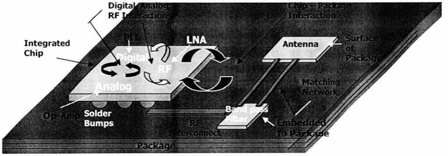
integrated Radio [image:14.525.58.517.281.441.2]Frequency System-On-Chip
implementations[1,2, 3],
depictedin Figure 1.1.Figure 1.1 The
System-On-Chip (SoC)
approach7.7.2 System-In-Package
(SiP)
implementationsEach of these domains
-digital,
analog, and RF circuitry posedifferent,
andsometimes conflicting demands on the fabrication process. RF circuitry, for example,
requires
high-quality
on-chippassives [4]. This inturn necessitates athick, low resistancetop
metal layerspecialized forinductors,
and ahigh-resistivity
substrate.Analog
circuitsdominantfactor for digitalcircuits. These incompatible demands amongthecircuitryofa
single systemhas led to the development of an alternate means ofintegration: while the
circuits are fabricated on different
dies,
which enables the use of different fabricationprocesses,
they
are integratedontothesamepackage,leading
toSystem-In-Package(SiP)
implementations
[5,6,7]
(3-Dstacking,Multi-chip
modules, etc.,Figure 1.2).RF Modules Horizontal Floor
[image:15.525.50.463.166.352.2]Planning
Figure 1.2 ThenstejiratedSysLem-In-Package
(SiP)
approachIn either approach, the complex interaction of signals across the analog, digital
and RF domains and the chip-package interactionsplace a huge burden on thepackaging
technology. The package exerts significant influence on the system performance, and
consequently, its accurate characterization is a necessity for the success of such RFIC
implementations.
1.2
Chip-Package
co-designThe rapid increase in circuit operating speeds, I/O pin count and
functionality,
challenges on the encompassing package.
Furthermore,
at radiofrequencies,
packageparasitics are nolongernegligible [8]:
BondWire
Lead Frame
(a)
Bond Wire Inductance
p j MutualInductanceandCapacitance
(b)
Figure 1.3
(a)
Interconnection of chip and package through bond-wires,(b)
parasitics associated withthechip-packageinterface.
Inductances ofthe order ofatenth of anano-henry and capacitances ofthe order
of atenthofa pico-faradcanhave ahuge influence on chip-performance.
Package bond-wires or solderbumps (Figure 1.3
(a))
aregenerally ofthe orderofafew nano-henry.
Other package associated parasitics that influence chip performance include
In addition, Electro-Static Discharge devices
(ESD)
present non-negligibleparasitic inductancesand capacitances,and
they
mustbe accounted forduring
thedesignprocess [17].
Traditionally,
circuit design and its packaging have been conductedby
differentgroups,
leading
tosub-optimal resultsfroman overallsystem performanceperspective. Inaddition, due to the high
frequency
complex inter-moduleinteractions,
'Packageaware'
design for RF transceivershas become a necessity.
Consequently,
the RFICindustry
hasaccepted a paradigm shift to chip-package co-design, whichinvolves concurrent design
ofboth chip and package
[9, 10],
where allthepackagingeffects are accounted forduring
thecircuit design process. Itmust be noted,
however,
thatmost of these parasitics havevery high tolerance
limits,
and this makes it almost impossible to accurately model orpredict them.
Therefore,
the performance ofRF circuits cannot be accurately predictedduring
design or simulation.1.3 Testing
andReliability
RFcircuits are prone to unique reliability
issues,
such as on-chip inductorfaults,
ground inductance
loops,
etc. In today's era ofintegration,
the RF core exists as a subsystem among many heterogeneous modules, and complexinter-module interactions(for
example, the digital circuitry can inject switching noise, which can be severely
detrimental to the RF core performance) make
testing
an even more critical issue. Inaddition, process faults and variations are only part of the list of probable causes of
variations and result in severe performance degradation. The quality factor ofon-chip
passives is abysmally low and unpredictable (30%): this can lead to soft-faults in the
circuits. To compound this
issue,
access to the RF core in such a complex system mayalmost prove impossible to achieve. Hence there was a pressing need to
develop
non-intrusive
testing
methods for RF circuits[11],
and thus was bom the Built-in-Self Test(BiST)
approach.The most important requirement of such
testing
is minimal intrusion.Any
probing device used should not alter the performance of the circuit
being
tested. Thisrequirement is a particularly challenging issue in RF circuits, since even small
inductances and capacitances can have a significant impact on the circuit. The other
requirements are low power, real estate and processing overheads, and reliabilityof the
testing
circuitry itself.Severalattemptshave been madeinrecent literaturetoaddress the problem ofRF
front-end reliability with the view of quantifying the effect of the various above
mentionedfactors on circuit performancethrough self-test,
thereby
attemptingtoimprovethe robustness ofthe RF part shipped to the end customer.
Many
approaches such as theloop
back technique proposed in[12]
and the end-to-end approach proposed in[13]
involve significant processingand real estate overheads since
they
require thepresence ofadditional DSP processing to achieve self test. Approaches such as the signature test
method proposed in
[14]
arevery computationallyintensive,
requiring a large amount ofoff line computation to estimate circuit performance. Current commercial approaches
test costin addition tovery largetest times to test RFparts.
Power-supply
current basedtesting [15,
16]
has been one ofthemore promising techniques, where thesupplycurrentis analyzed, and signature patterns quantify the performance degradation. None of the
above approaches have ledtoa
fully
integratedtesting
solutionfor RFcircuits,as yet.1.4
Necessity
forthis workHaving
laid-out the background in the previous sections, we now discuss certainoutstanding
issues,
critical to RFIC performance, which current approaches fail toaddress. Thiswork,as willbe shown,accountsfortheseproblems successfully.
While the chip-package co-design methodology and BiST approaches address
many issues
by
accounting for parasiticsduring
thedesign process[17],
development ofearly design techniques, etc.,
they
failtoaccountforthefollowing
problems:Widetoleranceranges of package parasitics: In currentapproaches,accounting
forpackage parasitics
during
thedesign process does not alleviate theproblem oftolerances. Since these parasitics are subject to wide variations that cannot be
predicted
during
the design cycle[18],
the performance of the circuitry maydegrade to sub-optimal levelsonce fabricated and packaged. More
importantly,
itleads to unpredictability of RFIC performance since these tolerances cannot be
accountedfor
during
simulation,and raises seriousreliability issues.Dependence ofESD protection on environmental conditions: ESD parasitics
can possesslarge tolerances,andthis leadsto the same problem mentioned above.
the RFIC's expected application, and any change in ESD devices necessitates a
completere-design ofthe circuitry.
Availability
of different packaging techniques: In any of the currentapproaches, a change in package alters the parasitic impedances and package
thermal characteristics;this necessitates modificationofthe existing
design,
or,inthe worst-case, repetition of the entire circuit design cycle. In either case, it
requires a new fabricationcycle, escalatingcosts.
Correction offaults: It has been already mentioned that no complete integrated
testing
solution exists for RFICs yet.Testing, however,
merely quantifies theperformance ofthe circuit, anddoes nothing to increasereliability. Ithas valuein
identifying
chips that degrade beyond acceptablelevels,
and ensures that thedefective product does not reach the end-user. In addition to process
faults,
otherfactors such as switching noise coupled from the digital module, power supply
coupling, etc. can degrade performance drastically. Quite evidently, a circuit
topology
that not just quantifies its performance, but also corrects itself in realtimewill bea
highly
desirablequality;itcan significantly improvereliability.Hence,
a circuittopology
thatdynamically
self-corrects itsperformanceto changingpackages and/or package parasitics, processfaults and variations,other soft
faults,
and ESD events, can
help
cut down design cycletime,
reduce cost and ensureoptimal performance under varying conditions. Such an approach is a major step
towards
immunizing
the circuit performance from package characteristics, and1.5
Preface
to this workThis work presents the first-ever successful attempt at self-corrective RF
circuits. It presents a unique architecture that enables on the
fly
modification in theperformance of RF circuits, and proves the concept
by
demonstrating
a completeimplementation. This architecture sidesteps the many obstacles that have prevented the
success of such a system so far.
7.5.7 Package Independence
The proposed architecture takes a significant step towards addressing a critical
bottleneck in today's RFIC
technology
-packaging effects. It progresses a step further
than merely modeling and characterizing package effects on the chip; it is an attempt to
render the chip independent of these effects, redefining the co-design paradigm. It
proposes a chip-level solutiontopackage
issues,
anddrastically
reduces chip-dependenceon accurate modeling and characterization of packages.
By
ensuring that a singlefront-end design will adapt itself
dynamically
to package parasitic variations, it cuts down ondesigncycle timesappreciably; italsofacilitates seamless package portability.
7.5.2 Fault Correction
As mentioned earlier, a low cost solution for RF self test, with a view towards
improving
reliability ofthe integratedcircuit parthas not yet been observed in publishedliterature. We propose atechnique to
drastically
increase RF integrated circuit reliabilitynot only
by
quantifying the performance ofthe RFcircuit on-chip butby
also correctingtheinputmatch of an LNA: it is the first steptowards thegrand vision of self-corrective
circuits.
Theend-resultisamethodologythat will quantify and correctthe performance of
the RFcircuit to accountfor processvariations and faults as well as package and passive
parasitic tolerances. This will not only make the RF circuit insensitive to package
parasitics but will also allow it to be portable between various packages while
dynamically
adjustingtheperformanceto accountfortheparasiticsin thenew package.1.53 Organization
A system for the self-correction of the input match for any RF front-end circuit
such as a Low Noise Amplifier
(LNA)
or mixeris described in Chapter 2. A noveltwo-tonal approach is presented wherein the
testing
process depends solely on the differencebetween two signals that pass through the same sensing circuitry, thus rendering the
entire technique insensitive to process, temperature, power supply and the precision of
the testsignal itself.
We demonstrate the application ofthis methodology to correct for shift in input
match
frequency
due to variations in parasitic inductances at the input ofthe LNA andprocess faults such as variations in gate-source capacitances. Thechoice ofthis particular
circuit isdeliberate: theLNA is the mostcritical circuit in any RF front end,becausethe
noise and the gain ofthis block most influences the noise figure of the entire front end.
Therefore,
thetestability
and reliability of this sub-circuit is of primeimportance,
toensure reliability oftheentire RFproduct. The circuitimplementation of all components
proposed technique is in itself very robust and will not be affected
by
variations inprocess or temperature. In addition to this, the method also involves low computational
and poweroverheads sinceit does not require the presence of aDSPcore. Thetechnique
uses input signals of moderate precision to test and correct the front-end circuit with
correctiontimes lowerthan30 microseconds. Chapter5 lists the summary and directions
for futurework.
This work is thefirststep towards the ultimategoalofpackage independent,fault
Chapter
2. ARCHITECTURE
2.1
Why
feedbackwill notwork2.2The 'Lockedloop' concept
2.3
Sensing
the Inputmatch2.4 Thenovel
'two-tonal'
approach
2.4 Signal processing 2.6The 'Tapped coil'
2.7 Self-correction algorithm
2.8 Merits ofthisarchitecture
2.1 Why
feedback will notworkTraditionally,
self-correction in analog circuits has been achievedby
usingvoltage or current
feedback,
where a part ofthe output voltage or currentis sampled andfed back to the input to achieve increased robustness with respect to process variations.
However,
this techniquehas several pitfalls when appliedto theRFdomain. In integratedRFfrontends, it is notalways possible to have accessto the output port ofthe individual
circuitto sample the output signal without
influencing
the performance ofthe circuit. Asmentioned in the previous chapter, the entire scheme must be minimally intrusive. In
addition to this, feedback components such as transformers, multipliers, etc., have wide
tolerances making the entire feedback system unreliable. This approach creates
significantly complex stability issues. In comparison to low
frequency
circuits, RFcircuits are
highly
sensitive to layout parasitics and mutual coupling effects. Metal traceparasitics, in theorderof a tenthofa nano-henry and tens offemto-faradsare no longer
negligible due to operations in theGHz domain. While stability is
inherently
difficulttocomplicates the
issue,
degrading
both reliability and predictability. RF circuits with nofeedback are
finely
balanced.Introducing
feedback will essentially re-define the entiredesign paradigm, and destroys our objective of rendering current RF circuits
fault-tolerant with minimal intrusion. It is thus seen that traditional feedback techniques
introduce significantdesigncomplexity,creating a needforthe redesignofthe RFcircuit
inquestion as a completefeedback system,withall itsassociated complexity.
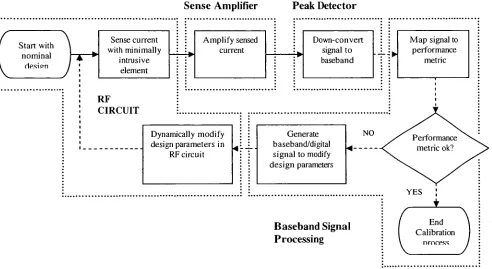
Sense Amplifier Peak Detector
Startwith nominal rlesipn Sensecurrent withminimally intrusive element Amplifysensed current Down-convert signalto baseband
Mapsignalto performance
metric
RF CIRCUIT
Dynamicallymodify designparametersin
RFcircuit
Generate
baseband/digital
signaltomodify
designparameters
Baseband Signal
[image:25.525.20.512.238.507.2]Processing
Figure 2.1 The self-correction methodology.
2.2
The
'Lockedloop'concept
Thecurrent work proposes an alternative technique that sensestheperformance of
the feedback circuitry. It is analogous to the locking1 achieved in Phase Locked Loops
(P.L.L.),
and hence theterminology
'locked loop'. The technique consists of an RFforward path where RF information (in the case ofthis work, the transient H.F. current)
correspondingto the circuit performance is sensed with minimal intrusion and amplified
to requiredlevels. As willbe described in greaterdetail in subsequent sections,since this
methodology does not pose anynoiserequirements,simple amplifiers with resistiveloads
can be used to achieve this gain. Also due to the robustness ofthe two-tonal technique,
(described in Section
2.4)
the actual numerical value ofthe gain does not influence theself-calibration. This amplified information is then down converted to base-band or DC
for further processing. The resultant baseband/digital signal quantifies the performance
metric under question and can be used as a BiST readout. This signal is then used to
modify the requisite design parameters in the RF circuit to correct for the variation in
performance without requiring any redesign of the original circuit. This idea is
summarizedin Figure 2.1.
Since the sensed RF information is not necessarily at the output node, the
proposed method lays much greater emphasis on avoiding intrusion into the circuit
performance. In addition tothis, the entire feedback path functions in the low
frequency
or DC domain
thereby
alleviating the stringent noise and aforementioned designcomplexity requirements that plague traditional high
frequency
feedback schemes. Aswill also be seen, this methodology differs from the traditional feedback concept in one
1
As in P.L.L.'s, the algorithm used in thisworkiteratesthrough a series ofpossibilities, and attheend of
each cycle computes if it has moved closer to the desired performance. Once a 'lock'
is achieved, the
more principal aspect: the output is neither sampled, nor fed-back to the input.
Instead,
the performance metric is measured,and a decision is made,
dynamically,
to modify (ifrequired) adesign parameterinthecircuit. This
'self-correction'
signalis inthe formof a
digital word, eliminating the potential problems of noise and precision. Both the input
and output ports ofthe circuit under consideration remain untouched. Since most ofthe
processing circuitry acts on low
frequency
signals, these circuits will also presentrelatively low overheads in the RF front-end. The
following
chapters of this work willdescribe the application of this methodology towards the self-correction of the
input-match of aLNA.
The objective of input match self-correction was addressed
by
a four foldapproach:
firstly,
to sense a signal which is indicative ofthe input match ofthe circuit;secondly, to process this signal appropriately into a formwhich quantitatively describes
the inputmatch ofthe circuit; thirdly,to use thisinformationto send a signalback to the
circuit where the match can be re-calibrated towards the desired value, and
finally
toprovidefor a mechanism in thecircuit which canadaptivelychange
Sn
inreal timebasedontheaforementionedfeedbacksignal.
2.3 Sensing
theInput Match
The first step in this processis to establish a means ofsensing some signal from
the circuit that, with further processing if required, will ultimately provide information
aboutits input match. RF circuits draw current from the power supply, which provides
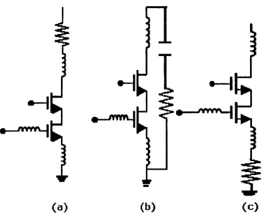
attributes. Some potential placements ofthesensing elementfor a single-ended Cascode
LNA areshownin Figure 2.2 [19]:
Placing
it in series with the drain inductor(Figure 2.2(a))
degrades gain,S22
andnoisefigure.
It can be placed in series with the bypass capacitor (Figure
2.2(b)),
which isnecessarilypresentinalmostevery RFcircuit2. Thisplacement
however,
degradesgain and
S22
significantly.Placing
it in series with the sourceinductor (Figure2.2(c)),
and re-designingtheinput match along with the sensingresistor results in minimal impact on
Sn
andnoisefigure.
f rtWA_||
/wy>
|
(a)
(b)
(c)
Fig
2.2 Potentialplacementsfor thesensing resistor2
RFcircuitshave bypasscapacitorstoprovidetheH.F.current,sincethepowersupplypathfromthe
[image:28.525.119.383.328.547.2]Further,
it is advantageous for this element to be a resistor, as opposed to aninductor or capacitor . From the above discussion it is evident that, in terms of minimal
intrusion,
placing a small resistorin series with the source inductorresults in the optimalsolution.
This approach creates a voltage indicative of the input match
frequency
withminimal intrusion on the circuit's behavior. It is possible to distinguish changes in the
current due to faults onthe output side ofthecircuit
by
usinga similar mechanism at theinput side ofthe next circuit in theRFfront-end chain (for example, the LNAis followed
by
a Mixer).By
co-designing the circuit with the sensing resistor, its impact on inputmatch canbe renderednegligible, and on noise figure and dynamicrange, minimal4.
The current variations in the LNA due to a shift in the input match are of small
magnitude (tens of uA).
Further,
since the resistor value is quite small (7 ohms, in thiswork), this voltage needs to be sufficiently amplified before further processing. The
voltagefromthe resistoris fedtoa source followerstage, which provides isolation to the
LNA fromtherestofthe sensingcircuitry.
2.4 The
novelTwo-tonal'approachAs will be described later in this chapter, it is the peak-to-peak amplitude of the
voltage across the sensing resistor that contains input match information and hence we
need toconvert this RF voltage into
DC,
which quantifies Sn. The sensed RFvoltage is3
The quantification ofanyperformancemetricin aRFcircuitgenerally involvessensingcertain signals at
multiple frequencies. The frequency dependent characteristics of capacitors & inductors complicate this
peak-detected and used for furtherprocessing.The circuitry that performs this operation
iscalledthe 'sensorchain', andisexplainedin Section 2.5.
One ofthe most importantrequirements ofthis process is to ensure that the
self-correction circuitry itself is extremely robust; process variations and faults in the
self-correction circuitry should not be mistaken for that of the circuit under consideration.
Towards this objective, a novel 'two-tonal' approach is presented, which, due to the fact
that its output is the difference of two signals that pass through the same overhead
circuitry, is extremely resilient. Thisapproachfurtheraltogether removes the
dependency
on absolute parameters like accuracyofgain,
linearity,
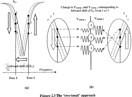
etc.Change inVTOnei andVTOne2correspondingto
leftwardshift ofSn from 1to3
Tone 1 Tone 2
[image:30.525.41.475.320.639.2](a)
(b)
For a given input match, the spectral output of this sensor chain is a steadily
decreasing
monotonic (almostlinear)
curve asfrequency
increases.Further,
thecurrent inthe LNA and hence the sensed voltage varies monotonically as the
SM
match is varied.Toascertaintheexact offsetthroughwhichtheinput
tuning
frequency
needs tobe shiftedand to render this technique independent of process, temperature and power supply
variations in the sensing circuitry
itself,
we use the two-tonal approach. The success ofthis methodology
depends,
among many other things, on the careful selection oftones.They
mustlieon either side ofthe desired input matchfrequency
(shown in Figure 2.3 asTone 1 and Tone
2)
such that theSn
variation lies within their bounds. For example,suppose theLNA is designed fora nominal match at3 GHzand theexpected inputmatch
variation is between 2.8 GHz and 3.2 GHz. Tone 1 mustbe chosen such that it is less
than 2.8 GHz andtone
2,
greaterthan 3.2 GHz. This selection procedure ensures that themonotonocityofthe sensed voltage versus input match isconsistent across the
frequency
spread (2.8 GHzto 3.2
GHz,
inthiscase).Two test signals corresponding to the above frequencies are applied to the LNA
one after the other. Each signal passes through the same sensing circuitry and these
outputs
(Vtonei
andVtone2)
are peak detectedand stored ontwo capacitors.Decreasing
theinput matched
frequency
increases the amplitude ofthe first tone(Vlonei,
as depicted inFigure 2.3
(b))
and decreases the amplitude of the second signal(V,one2,
as depicted inFigure 2.3 (b)). The difference between
V,onei
andVtone2
provides a measure oftheshift inSi
i, andhencethefrequency
offsetby
whichinput matchneeds to bemoved tocorrect itThefact that bothtones passthrough the same sensor and peak
detector,
and it istheir difference that is processed, renders this processrobust.
Any
unexpected variation,forexample, high ambient
temperature,
will affectboth the tonal-signals equally, and thesubtracted signal will retainits faithfulness. It is shown in Chapter 4 that this method is
insensitive toprocess variations, temperature and power supply variations.
Furthermore,
this differential method of ascertaining input match
frequency
renders the techniqueimmune,
forexample, eventoa 50% variation inthegain ofthe sensor, tolerances in thesensingresistor value ortheprecision ofthe inputtestsignal itself. Itmust bementioned
at this point that the use of athird tone at the desired input match
frequency
(3GHz,
inthe above example) can also provide quantification ofthe magnitude ofthe input match.
This information can be used to correct the magnitude of the match if it falls below
acceptablelevels.
2.5 Signal Processing
As mentioned in theearlier sections, the sensed voltage from the LNA is quite
small in magnitude and needs to be amplified. It is then converted to DC
by
peak-detecting
the signal.Consequently,
any amplification of the voltage signal mentionedabove need not be noise-freeor low-noise5. This allows one to useresistors, and simple
single-stage gain configurations (the push-pull amplifier, or the Common Source
amplifier used in this work) can amplify the signal up to a few hundreds of millivolts.
5
We would otherwise be faced with the amusing conundrum of requiring LNAs to quantify LNA performance.Itshould alsobementionedthatusing othervariantsofRFamplifiers(withinductors) in the
Robustness canbe accomplished withfeedback inthe amplifier(source
degeneration,
forexample), but after extensive simulations, it was deemed unnecessary due to the
resilience of the 'two-tonal' approach.
Further,
the amplitude of the test signal can beconsiderably higherthan thetypical input signal amplitudes to the
LNA,
withinthe limitsofits
linearity
and dynamicrange.This in turnbrings downtheamplification needs ofthesensing amplifier. This signal isthen input to a peak detectorwhich outputs aDC signal
inproportion to theinputmatch oftheLNA.
The processing circuitryrequired forthiswork consists of:
PMOS Source-follower DC Buffers
RF Sense Amplifier DC Subtractors
RF Peak detector
(PD)
ComparatorsStorageelements
(capacitors)
Digital logic andclockingThe self-correction algorithm, explained in detail in Section
2.7,
willelaborate on the
functionality
of each circuit. The output (foreach tone) from the peakdetector is stored on different capacitors, and the subtraction is performed
by
op-amps.The op-amps draw theirinputsthrough buffers tominimize chargeloss in thecapacitors
and isolate the peakdetection circuitry. The rest ofthe processingcircuitry iscomprised
ofcomparators, again derived from op-amps, and digital circuitry and clocking. As will
be seen
later,
a number oftiming
pulses are required for this process, and in this work,they
are all derived from a global clock signal. The final output of the processingcircuitry will be an n-bitdigital word, which willbe fed to theLNA. It will also be seen
technique. It mustonce againbe emphasizedthat none ofthe aforementionedprocessing
circuitry hashigh-precision/ accuracyrequirements.
2.6
The 'Tapped
coil'With the above setup, the last piece required to complete the 'puzzle' is a
mechanism intheLNA which, while notrequiring anymajordesignmodifications, must
allow for dynamic input match changes. The input match ofthe inductively-degenerated
cascodeLNA is given
by
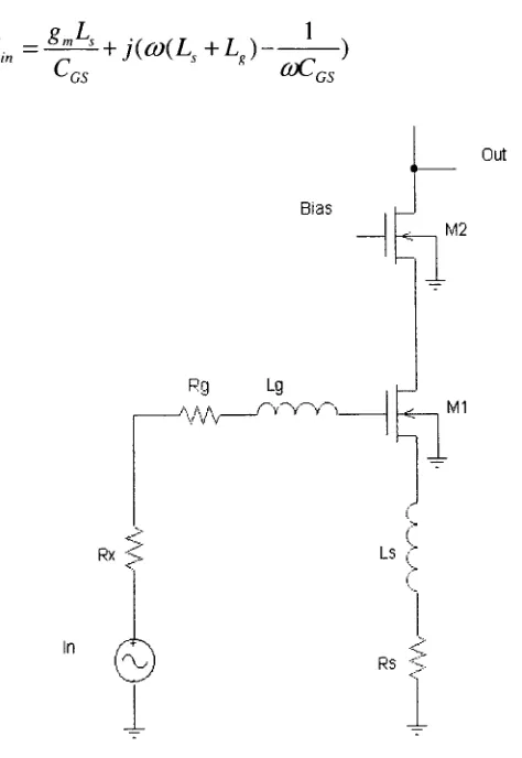
[20]:Zm=-^
+j(ay(Ls+Lg)--L-)
C,
GS -GSRx
Bias
Rg Lg
a a.
/^ /-yvv^
Out
M2
M1
Ls
[image:34.525.156.393.268.612.2]Rs S
gm is the transconductance of
M]
(Figure 2.4). It is controlledby
the size(W/L)
and the DC current through Mi.However,
varying gm to vary theinput match will also result in other undesirable changes, like power
consumption, gain,dynamic range,etc.
Ls
is thesource coil ofthe LNA. It isresponsible forthe magnitude ofthematch. In other words, if correctly
balanced,
atthe resonantfrequency,
theeffectiveinput impedancewill be a pure resistive value of:
ry Ofll s r *-C5
Hence varying
Ls
will notvarythe inputmatch frequency.CGS
isthe gate-source capacitance ofMi.Adding
additional capacitance inseries with
Lg
will enable us to controlSn
frequency. In order to bedynamically
adjustable, a varactor is needed, but unfortunately, MOSvaractors in most RFIC processes
(IBM,
TSMC,
both 0.25 pm and 0.18pm processes) musthave one end grounded. Hencethecapacitorhas to be
used in parallel (from gate of
M,
to ground), ratherthan in series.Using
the capacitor in series has the undesirable effect ofchanging the real part
of the input impedance too6, and after numerous simulations it was
concluded that a varactor can be used only if a transformer is used to
couplethe input sourceto theinput port ofthe LNA.
6
This leadstoacompleximpedancenetwork,whichwhentransformedinto itsseriesRLCequivalent(after
Lg
is the gate coil oftheLNA,
and varyingthis element changed onlytheSn
match frequency. In this work,it is thegate coil that acts asthe vehiclethatcompletestheself-calibration 'locked-loop'.
In ordertoadaptively movethe input match ofthe
LNA,
the gate inductorvalueismade variable
by
tapping
it at several points. Package parasitics introduce additionalinductance (with very large tolerances) at the input pad ofthe LNA (for example, bond
wires). In this work, we showthatprocessfaults andtheseparasitics canbe accounted for
inreal-time
by
re-calibratingthe inputcoil ofthe LNA. Thistechnique alsofacilitatestheuse ofthe LNA in different packages withdifferent parasitic
inductances;
thecircuit canre-align itselfto theoriginal inputmatch onthefly.
The gate coil
(Lg)
is designed fora nominal value andthen tapped off atdifferentintervals in its outer-most turn, with each
tap
leading
to a switch.By
including
theinterconnects and switch capacitance in the design process, thiscoil canbecharacterized
togive accurateinductance values. Basedon which switchisturned on, one and only one
tap
of the coil will be shorted to the input pad of the LNA (Figure2.5),
and thistap
determinesthe inputmatch oftheLNA.
2.7
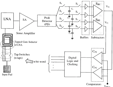
Self-correctionalgorithmIn this section, we describethe mappingofthe abovemethodology to the specific
purpose ofcorrecting the input match of a LNA. The circuit architecture is depicted in
' ///
.1. Buffers Subtractors
\TappedGate Inductor
,'ofLNA
\
Tap
Switches "^ntapS)
^-_
yX^7n-bit word
Input Pad
Digital
Logic and
Clocking
[image:37.525.47.478.56.388.2]Comparators
Figure 2.5 Circuit Architecture forcorrection ofLNA inputmatch
frequency
Stepl:
Having
chosen the two tones (tonel and tone2) to be used for the input signals,the switch connecting the first
tap
ofLg
is closed, and a test signal with afrequency
oftonel is applied to the inputoftheLNA.
Step
2: The resultant output ofthe PD is stored in capacitorC]
through switch Si.Si
isnowturnedoff.
Step
3: Repeat step 1 for tone2, and storethe resultant output in capacitor C2. Theswitchdischarge path, their leakage is minimal and can be reduced to negligible values
by
choosingappropriatecapacitances.
Step
4: The secondtap
ofLg
is now closed(changing
the value ofLe
and hence movingthe input match) and the above process is repeated, storing the P.D outputs in different
capacitors
(C3
and C4). At this stage of the process, we have stored the output of thesensor chain for two tapsofLg.
Step
5: SwitchesS5
throughSs
areturnedon simultaneously,connectingthecapacitorstothe buffers. For both tapsof
Lg,
the tonal difference amplitudes are calculatedby
meansoftwosubtractors
(Vti
andVT2).Step
6: NowVTi
andV-n
are comparedindividually
withV[DEal,
whereVIDEAl
is thevoltage difference of the two tones for the desired input match. Although in this work
Videal
isafinite valueforease ofimplementation,
itcan beensured thatViDEAL
is 0Vby
slope-correctingthe gain ofthe sense amplifier with respectto
frequency,
thereby makingthecalibration independentof a fixedreference voltage.
Step
7: IfVT)
is closertoV1DEAL
thanVj2,
the firsttap
ofLg
is connected to the inputpad, and self-calibration process is complete. If
VT2
is closertoVIDEAL,
then steps 1 to 6are repeated, this timeforthe second and third taps of
Lg
instead ofthe first and secondtaps.
Step
8: The self-calibration will be complete whenVT(j)
will be closer toViDEAL
thanVT(i+i)
(this is true sincethe amplitude ofthe sensed voltage is monotonic as the inputmatch
frequency
is varied). Ifthis conditionneveroccurs, then thelasttap
ofLg
ischosenAll the switches needtobe turnedon for specificintervals periodically, and these
pulses are derived from a global 2 MHz clock, using
decoding
circuitry. The algorithmdescribed above follows the linear-search model. Although not maximally efficient in
termsofthe time taken,thismethodology provides adequate recompensein return, in the
formof simplercircuitryand ease ofimplementation.
2.8 Merits
ofthis architecturePerhapsthe most importantcriterion of anytest-and-correct circuitry is to
ensure that any faults and variations of the test circuitry itself will not
mistakenly
identify
non-existent faults. The two-tonal approach, coupledwith simple processing circuitry that does not use any feedback or
inductors greatlyminimizestheprobabilityofthat occurrence.
The 'locked-loop' methodology eliminates all the associated complexity
of atraditional feedback scheme,while retainingitsusability.
It requires minimal overhead circuitry.
It requires no DSP cores or processor requirements, which is typical of
many RFtestmethods.
It doesnot require A-Dconversion or analog memorycells,and consumes
little power. The entire processing circuitry, with the exception of a few
latches,
canbeturned offcompletelyoncetheprocess iscomplete.The entire time taken for the self-calibration depends on the number of
processing time. This compares very
favorably
to times takenby
currentcommercial test schemes
[8],
wherein thetesting
period itself is in theorder ofhundredsof milliseconds.
The only intrusion in this methodology is the small sensing resistor (7
ohms in this work). The value of the resistor is
flexible,
and can bereduced further at the cost of
increasing
thegain of the sense amplifier.This should not pose majorproblems sincecascadingan extra stage ofthe
amplifieris straightforward andincreases gain significantly.
By dynamically
adaptinga single design tovarious package variations andfacilitating
package portability, it cuts down on design cycle time, andreduces the dependence of circuit performance on accurate package
characterization and modeling.
The architecture described above carefully side-steps many potential
roadblocks in sensingand correctingthe performance ofRFcircuits. The simplicity
and ease of
implementation,
which is thesubjectofthenext chapter, istestimony
toChapter
3.
CIRCUIT
IMPLEMENTATION
3.1 Single-ended1.9 GHz LNAwith
Sensing
resistor-3.1.1 INA Design
-3.1.2 TappedGate coil 3.2 The Sensorchain
-3.2.1 Source Follower
-3.2.2Amplifier
-3.2.3 Peak Detector 3.3. Low
frequency
& Digital processing3.4.
Timing
3.5. Limitations
3.6. Implementation
Summary
The previous chapterhas described the general methodology that can be adapted
to specificRFcircuits.
Typically,
RFfront-end circuitry is interfacedto the outside world(antenna)
through aLow Noise Amplifier (LNA).Consequently,
it is theLNA that formsthe physical connection between the package and the integrated circuit, and package
parasitics have a direct impact on its performance.
Further,
the LNA is the most criticalblock of any front end since its noise and gain affects the performance of the entire
system. Thus it becomes an ideal choice for this work
-self-correction can be
demonstrated for both processfaultsand packagetolerances/flexibility.
The Single-ended Cascode LNA is perhaps one the most widely used LNA
topologies [17]. Although the balanced
(differential)
topology7offers more advantages,
the single-ended LNAenjoys popularityfor its ease of
implementation,
and the fact thatit possesseslesserreal-estateand powerconsumption requirements.
7
The self-correction methodology described in preceding chapterhas been applied
to a 1.9 GHz CMOS Single-ended source degenerated narrow-band cascode LNA. This
chapter
discusses,
indetail,
the implementation of the LNA and all of the associatedprocessing circuitry. All circuitry has been designed and laid out in the IBM 6 Metal
layer 0.25 pm RFprocess
(CMOS6RF)
with a2.5 Vpower supply.3.1
Single-ended
1.9 GHz LNA
withSensing
resistorThe first stage of a receiveris
typically
alow noise amplifier(LNA),
whose mainfunction is to provide enough gain to overcome the noise of subsequent stages. Aside
from providing this gain, while adding as little noise as possible, an LNA should
accommodate large signals without
distortion,
andfrequently
present a specifiedimpedance,
usually 50ohms, to theinput source.The RF circuit in question, in this case the
LNA,
needs to be co-designed toaccommodate for two factors. It must accommodate a minimally intrusive sense
mechanism that will allow the extraction of its match
information,
and should alsoprovide for a mechanism to recalibrate the match if deemednecessary, toobtain optimal
performance.
3.1.1LNA Design
The sensing mechanism in the LNA is provided for
by
a7 ohm resistor(Rs)
thathas been placed in series with thesource
inductor,
in the return current path ofthe LNA.As explained in Chapter
2,
this is the point of least intrusion for the resistor, and thevalue is theoptimal solution for the trade-off
between reducing the degradation of noise
figure and dynamic range ofthe LNA on one side and achieving sufficient sensitivityto
be able toadequately detectvariations in the input match. Although
Sn
is alsodegraded,
the LNA can be designed with the resistor in the equation for input match to get back
most ofthe input match. Due to the differential nature ofthe methodology described in
previous sections, the success ofthe calibration approach isunaffected
by
the tolerancesin theactual value oftheresistance.
LNA Inpul Pad
*. To Source
Follower
Y
NMOSSwitches
[image:43.525.116.406.247.500.2]RS=7D
Figure 3.1SchematicofCascode LNA withtappedgateinductor
The schematic of the LNA is shown in Figure 3.1. The addition of the sensing
resistancechangesthe inputmatch equation,adding twoextra terms:
Z,
=^^
+j{co(Ls
+L))
Co-design with
Rs
involvesdesigning
Sn
usingthis modified equation. Atresonance, theimaginary
part oftheimpedancecancels out since:COLGS
aX-csresulting in aninputresistance of:
'-'GS
The value of
Ls
required to achieve a 50 ohm match is 0.75 nH. The inputtransistor ofthe LNA forms a current mirror with the transistor
(M3)
ofthe biascircuit.The width ofthe biascircuit transistor is chosen tobe one-tenth ofthe inputtransistor to
minimize power overhead of the bias circuit. The supply voltage and a reference
resistance
(Rbias)
set the current through the left-hand side of the current mirror inconjunction with the Vgs of the input transistor. Resistance
R2
must be made largeenough so that its noise contribution can be ignored [20]. Since the input resistance is
50ohms,
R2
ischosen tobe 5 Kohms. An external gate-source capacitance(CGsx,
Figure3.1)
with a value of0.6 pF has beenincluded;
thisresults in a nominalLg
value of9 nH.The outputload
(Ld
andCL)
valueswere chosen toresonateat 1.9GHz.1
/=
2k^L~Cl
The DC
blocking
capacitorischosento be 30pF sothat its impedanceat 1.9 GHzis negligible. A power supply bypass capacitor, as discussed earlier, of 30 pF was
input-side of the LNA only, no impedance-transformation is needed at the output node ofthe
LNA. It is
directly
connected, through aDCblocking
capacitor, to theoutput pad.3.1.2 Tapped
Gate
CoilThe self-correction ofthe LNA in the present case has been achieved
by
usingadigitally
tapped gate inductor at the input of the LNA. Thedigitally
tapped inductor asshown in Figure 3.1 consists ofNMOS switches that are connectedto the gate inductorat
various points in its outermost turn and can be used to
tap
into various sections ofthegate inductor.
Therefore,
by
turning
the switches on oroff, the value ofthe gate inductorcanbevaried,
thereby
varyingthefrequency
of match.It is of significancethat the inductorand its associated parasitics be characterized
accurately. Thegate inductorwas laidout and simulatedusing ASITIC [21
]
todetermineNMOS Switch
/ input
[image:45.525.123.458.374.610.2]^
padFigure 3.2 Layoutofgate coil.The dimensionsare: radius=220
p.m,width of metal
the parasiticinductances andcapacitances associated with the structure (Figure 3.2). This
structure includes all the metal strips used for various interconnections up to the input
pad. The NMOS switches are chosen to haveaW/Lof
68um/0.25um,
providingan idealbalance between on-resistance and device capacitance8. The five
'taps'
of the coil are
connected to the NMOS switches, and are referred in subsequent sections as tapl, tap2,
and soon, upto tap5.
Tap
no. InductancevalueCorresponding
Si
i freq.1 7.4nH 1.7 GHz
2 8.1 nH 1.8 GHz
3 (nominal value) 9nH 1.9 GHz
4 10nH 2.0 GHz
5 11 nH 2.1 GHz
ible3.1 Thetappet coil values and cc^responding
Sn
frequenportl
9.09 nH
:mm_
120fF
182ohms
5.01 ohms
AA/V
f_res= 6.42 GHz
9nd
Q = 11.20
port2
96.2fF
247 ohms
gnd
K7 ^7
Figure 3.3Pi-modelforthegate coil when
tap
3 isturned on(nominalvalue)8
The LNA is then co-designed to account for these parasitics (the Pi-model from
ASLTIC is used for the gate coil, Figure
3.3)
as well as the parasitic capacitances andfinite on-resistance associated withtheMOS switches. Thetapped gate inductor designed
in this workhas five taps, providing inductance values between 7.4nH and 1 1 nH (Table
3.1). Thesetaps were chosen suchthat the inputmatch oftheLNAcanbe variedfrom 1.7
GHz to 2.1 GHz in stepsof0.1 GHz. Since all the taps have tobe connected to a single
inputpad,care has beentaken to:
Ensure that the interconnects are placed at least three turn widths away
from thecoil.
All the taps have been drawn out with perpendicular metal strips that are
widerthan the width ofthe inductortominimize additional inductance.
In addition to the above precautions, the whole structure was simulated in ASFTIC to
accountfor any mutualand additional inductances.
The input to the NMOS switch array is a digital word that dictates which one of
the 5 tapsis to be turned on,
thereby
fixing
the value ofthegate inductanceofthe LNA.Forexample, iftheparasitic inductance ofthepackage
increases,
thetap
cantherefore beshifted, reducing the amount ofon-chip gate
inductance,
thus restoring thefrequency
ofinput match for the LNA. The resolution or range of correction can be improved
by
3.2 The
Sensor
chain3.2.1
Source
FollowerThe voltage across the sensing resistor
Rs
is then fed to a PM0S source followerwith aresistive load. The sourcefollowerserves to isolatethe LNA from any processing
circuitrythatwill follow and also provides arelatively broadband interface to transfer the
sensed signal acrossthe sensingresistorto the processingcircuitry. The size ofthesource
followertransistor is kept small so thatit presents a negligible capacitance at the source
nodeofthe LNA. Thiscapacitance isequivalent to addingadditionalinterconnect related
parasitics atthesource node ofthe
LNA,
andit does not affect the LNAperformance.Itsoutputis AC-coupledto the amplifier stagethrough aDC
blocking
capacitor.Vdd
ffomfts
~p-
-R,
-Ir
Ri*2i
4[Z
Rb2|
HL
to peak detector
Figure 3.4 Thesourcefollowerand amplifier
3.2.2 Amplifier
The magnitudes of voltage variations across
Rs
corresponding to changes in theamplitude of the test signal can be considerably higher than typical LNA
inputs,
theresultant gain requirements ofthe amplifier are verymoderate. In addition tothis, due to
the absenceofanyrestrictions on noisefigure ofthesensed signal simple common source
amplifiers with resistive loads can be used to achieve the required amplification.
Push-pull amplifiers can provide very high gain, but need extensive bias stabilization for a
stable operation. Two cascaded common source stages have been used to construct the
amplifierbecause it ispossibleto AC-couple the sensed signal fromone stagetoanother,
while providing independent DC biases to each stage. The minimum required gain from
this amplifier was eight. Simple resistive bias was found tobe adequately stable, since it
depends on the ratio of two resistors9.1 K ohm resistive loads have been used because
they
provide the required gain, while also presenting optimal source impedance to thepeak detector that follows. No feedback has been incorporated into the amplifier due to
the inherent robustness ofthe two-tonal approach10. As will be shown in Chapter
4,
aslong
as the amplifier can provide a minimal gain at all process, supply and temperaturecorners, variations in the numerical value of the gain will not affect the successful
calibration of the RF circuit. The amplifier and the source follower form the sense
amplifier
(SA,
Figure2.5,
Figure 3.4). Since more common source amplifiers can becascaded asdescribed above
(making
itpossibleto achieve highergains), it mayeven be9
The resistive pair mismatchdata in the IBM PDK lists the percentage mismatchfor various resistance pairs. Bychoosingappropriate widths forthepolysiliconresistors,mismatch canbe minimizedtolessthan
2-3%.
10
The amplifier was designed with source-degeneration feedback & drain-gate resistor feedback, and
possible to reduce the value ofthesensing resistor
by
a few ohms to take advantage oftheavailable gain, further minimizingintrusion ontheLNA.
3.2.3 Peak Detector
A standard half-wave diode
(inverting)
voltage doubler (Figure3.5)
has beendesigned to peakdetect the sense amplifier's output. The diodes are current-biased inthe
linearregion forthe range ofits input signals. Since the P.D output has to be stored on
four different capacitors, the output capacitor is duplicated fourtimes
(C\
-C4) andthey
are connected to node
N]
(Figure3.5)
through transmissiongates (S1-S4). This eliminatesthe need for external memory capacitors. The transmission gates are driven
by
digitalpulses generated in the digital circuitry. The ratio ofinput and output capacitance values
was chosen tobe 5:3toensure optimum chargetransfer.
^ (SeeFigure
2.5)
rtvitctrt*
S5-S9
Figure 3.5 Half-wave
inverting
diodePeak DetectorThis peak detector was robust across process, supply and temperature variations.
The drift in diode characteristics will be canceled out sincethe difference oftwo signals
between on-resistance and capacitive parasitics. For this application, the on-resistance is
not a critical issuesince we can always allocate extratimeforthecapacitorstocharge.
The entire sensor chain is also provided with a robust high
frequency
return pathby
connectinga 30pF capacitorbetweenpower supplyand ground.3.3
Low-frequency
&Digital
processingThe outputs of the peak detector are fed to the two subtractors
(Sbi
andSB2,
Figure
2.5)
through unity gain buffers. Due to the presence of thebuffers,
the peakdetectorcapacitors have nodischarge path (to discharge the capacitors when required, a
switch is connected across each capacitor and ground. It is only turnedon at the end of a
correction cycle)
thereby
retaining all their charge except leakage. Since the signalshandled
by
the unity gain buffer and the two subtractors are DC voltages, a standardfolded cascode op-amp (Figure
3.6)
is adequate for both these functions. The foldedcascode configuration is chosen because of its high output
impedance,
high gain andinherently
highoutput swing forthe given process.The op-amp is biased using a wide swing cascode current mirror with an external
bias reference of 1 V.
Accuracy
requirements arefairly
relaxed since the op-amps areused in a feedback system at DC levelsonly. The op-ampwas designedto have a gain>
1000,
a power consumption <lmW,
and was compensated with a 7 pF capacitor. Thesubtractors were designed to have a gain of
3,
with the corresponding feedback resistorthese resistors", it isnot subjectto huge variations.Thetwo comparators
Cpi
andCp2
arealso obtained
by
using the folded cascode configuration. The outputs ofthe comparatorsare usedtodrive standard digital logic.
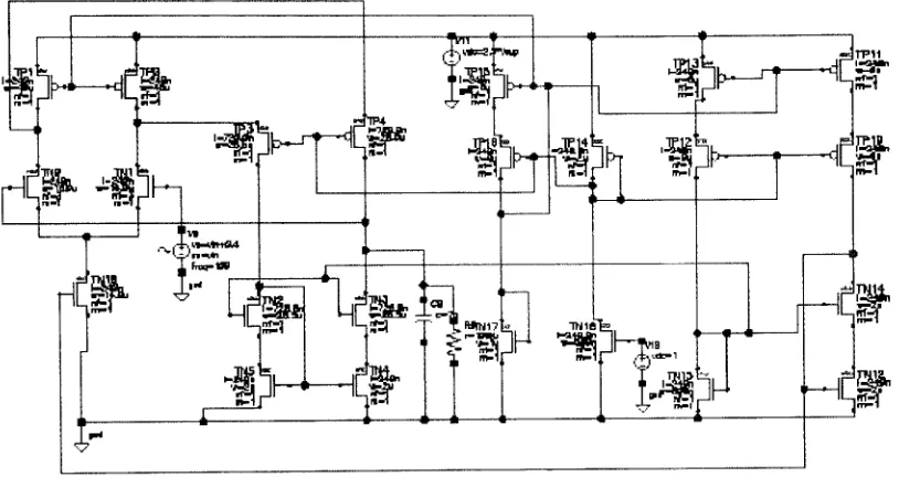
IJ^HD
d
m
-&, -T^i tw*fa
J^-r|
"CST WjWi^ZT^ 7P11ILilM T T."iw"^,
A 1 1 1 1
<
M
'-HI<S
; -ITTJI
Figure3.6Folded-cascode op-ampconnected as aunity-gain amplifier with current
<