Zirconium Doped Zinc Oxide Thin
Films Deposited by Atomic Layer
Deposition
STEPHANIA HERODOTOU
PhD Thesis
The University of Liverpool
School of Engineering
Faculty of Science and Engineering
To my mother and my late father who I never met but he was always my inspiration
Acknowledgments
I express my gratitude to everyone who supported me throughout the course of this PhD study. I would like to thank my supervisors Dr. R. Potter and Prof. G. Tatlock for their support and guidance. I would also like to thank Dr. K. Abrams from the NanoInvestigation Centre in Liverpool for providing TEM images of the current samples, and Dr. R. Treharne along with Prof. K. Durose from Stephenson Institute for Renewable Energy for providing guidance and the equipment for the spectrophotometer measurements. I express my warm thanks to the academic and technical staff of the Material Science team, who help me and provided me with the facilities being required for this research. I would also like to thank SAFC Company for providing the ALD precursors for my study.
Abstract
Doped zinc oxide is of interest as a transparent conductive oxide (TCO), due to the abundance of its major constituents, its low resistivity, high transparency and wide bandgap. The current work focuses on the properties required for TCO applications including resistivity of ≤10-3
Acknowledgment……… Abstract……….. Table of Contents ... List of publications………. Notation……….. Chapter 1 ...
Introduction ... 1
Chapter 2 ... Literature Review ... 6
2.1 Properties of Zinc Oxide ... 6
2.1.1 Crystal structure ... 7
2.1.2 Electrical and Optical properties... 9
2.1.2.1 Optical emission background... 9
2.1.2.2 ZnO bandgap... 13
2.1.2.3 ZnO stimulated emission ... 14
2.1.2.4 ZnO defects ... 16
2.2 Applications of ZnO ... 17
2.2.1 LED ... 19
2.2.2 UV photodetectors ... 19
2.2.3 Metal-Insulator-Semiconductor ... 20
2.2.4 Solar cells ... 21
2.2.5 TCOs ... 22
2.3 Growth techniques ... 26
2.3.1 CVD ... 26
2.3.2 Magnetron Sputtering ... 27
2.3.3 MBE ... 28
2.3.4 Sol-gel ... 28
2.3.5 PLD ... 29
2.4 Doping in ZnO ... 30
2.4.1 Doped ZnO films ... 30
2.5 Atomic Layer Deposition ... 38
2.5.1 ZnO deposited by ALD ... 43
2.5.2 Doped ZnO deposited by ALD ... 47
2.5.3 Zirconium in ALD ... 47
Chapter 3 ... Experimental processes ... 49
3.1 Introduction ... 49
3.2. Ellipsometer ... 49
3.3. Atomic Layer Deposition ... 54
3.4. Four-Point probe ... 61
3.5. Hall Effect measurements ... 64
3.5.1. Background information ... 64
3.5.2. Measurement information ... 68
3.6. Photoluminescence ... 71
3.6.1. Background information ... 71
3.6.2. Measurement information ... 72
3.7. UV-Vis Spectroscopy ... 77
3.7.1. Background information ... 77
3.7.2. Measurement information ... 82
3.8. X-ray Diffraction ... 83
3.8.1. Background information ... 83
3.8.2. Measurement information ... 89
3.9. X-ray Photoelectron Spectroscopy ... 92
3.10. Transmission Electron Microscope ... 98
3.11. Atomic Force Microscope ... 101
Chapter 4 ... Effects of Zr doping on the microstructure of ZnO films ... 105
4.1. Introduction ... 105
4.2. Effect of growth temperature on un-doped ZnO... 106
4.3. Zr-doped ZnO microstructure ... 113
4.4 Orientation shift ... 133
4.4.1 Orientation shift by strain ... 137
4.4.2 TEM study of the thicker doped film... 143
4.5. Conclusion ... 147
Chapter 5 ... Electrical properties and chemical state of ZnO and ZnO: Zr ... 149
5.1 Introduction ... 149
5.2 Zr-doped ZnO films electrical properties ... 154
5.2.1 Resistivity, carrier density and mobility of the ZnO: Zr films ... 154
5.2.2 Carrier density increase at low Zr doping levels ... 156
5.2.3 Carrier density decrease at high Zr doping levels ... 159
5.2.4 Carrier mobility reduction with Zr doping ... 160
5.3.2 Refractive index ... 163
5.2.5 Improvement of electrical properties ... 164
5.3 Degeneracy of the ZnO films ... 168
5.4 Chemical state ... 172
5.4.1 XPS spectrum analysis... 173
5.4.2 Chemical shift ... 179
5.6 Conclusion ... 182
Chapter 6 ... Optical properties of ZnO and Zr-doped ZnO films ... 184
6.1 Introduction ... 184
6.2 Spectrophotometry ... 185
6.2.1 Transmittance... 185
6.2.2 Drude model calculations ... 191
6.2.3 Optical bandgap calculation... 193
6.2.4 Conclusion of the Spectrophotometry results ... 195
6.3 Photoluminescence ... 195
6.3.1 PL on un-doped ZnO films ... 195
6.3.2 PL on ZnO: Zr samples ... 212
6.3.2.1 The PL peaks origin ... 218
6.3.2.2 Thickness effect in the PL emissions ... 224
6.3.2.3 Energy increase of the dominant emission in doped films ... 225
6.3.2.4 Optical gap modification... 227
6.3.3 PL Conclusion ... 232
Chapter 7 ... Conclusion ... 233
7.1 Main outcome ... 233
7.2 Future work ... 236
References ... 238
List of publications
Herodotou, S., Treharne, R. E., Durose, K., Tatlock, G. J., & Potter, R. J. (2014). The effects of Zr doping on the optical, electrical and microstructural properties of thin ZnO films deposited by ALD. Submitted paper to Thin Solid Films as a „SI: TCM 2014 article‟.
Notation
Arabic
A Absorbance (%)
Aw Atomic molecular weight (g/mol)
B Magnetic Field (Telsa)
d Lattice spacing (Å)
D Grain size (nm)
e Electron Charge (C)
E Formation energy (eV)
F Structure factor (unit-less)
FC Texture coefficient (unit-less)
ħ Planck constant (Js)
I Intensity (MW cm-2)
I0 Integrated intensity (a.u.)
IC Electric Current (A)
m* Effective mass (kg)
m0 Electron mass (kg)
m0* Effective mass at the bottom of the CB (kg)
meh* Reduced effective mass (kg)
mh* Hole effective mass (kg)
NA Avogadro‟s number (1/mol)
NC Mott critical density (cm-3)
ne Electron Carrier Concentration (cm-3)
R Reflectance (%)
Rs Sheet Resistance (Ω/☐)
S Surface energy (Jcm-2)
r0 Exciton distance (Å)
rs Radius ratio of Bohr over exciton (unit-less)
t Thickness (nm)
tC Critical thickness (nm)
T Temperature (°C)
Tr Transmittance (%)
TU Optical Thickness (Å)
VH Hall voltage (V)
Z Atomic number (unit-less)
Greek
α Absorption coefficient (unit-less)
αr Bohr radius (Å)
α0 Hydrogen Bohr radius (Å)
αm Monolayer thickness (Å)
αnp Non-parabolicity parameter (eV-1)
αZn Auger parameter for Zn (eV)
ε Strain (%)
ε0 Vacuum permittivity (Fm-1)
θ Bragg‟s diffraction angle (°)
λ Wavelength (nm)
μ Carrier mobility (cm2V-1s-1)
ρ Resistivity (Ω·cm)
ρd Density (kg cm-3)
τ Relaxation time (s)
Φ Work function (eV)
ωp Plasma frequency (cm-1)
Acronyms
4PP Four Point Probe
ALD Atomic Layer Deposition
ALE Atomic Layer Epitaxy
AZO Al-doped ZnO
BGN Bandgap narrowing
BM Burstein-Moss
CB Conduction Band
CDS Chemical Database Service
CVD Chemical Vapour Deposition
DC Direct Current
DEZ Diethylzinc
DFT Density Functional Theory
DSSC Dye Sensitised Solar Cells
ECR Electron Cyclotron Resonance
EDS Energy Dispersive Spectrometry
EHP Electron-Hole plasma
EPES Elastic Peak Electron Spectroscopy
FESEM Field Emission Scanning Electron Microscope
FET Field-Effect Transistor
FFT Fast Fourier Transform
FIB Focused Ion Beam
FTO Fluorine doped Tin Oxide
FWHM Full-Width at Half Maximum
GZO Ga-doped ZnO
IMFP Inelastic Mean Free Path
ITO Indium Tin Oxide
LD Laser Diode
LPCVD Low Pressure Chemical Vapour Deposition
MBE Molecular-Beam Epitaxy
MEMS Micro-Electro-Mechanical Systems
MOCVD Metal-organic Chemical Vapour Deposition
MQW Multiple Quantum Wells
MIS Metal-Insulator-Semiconductor
MSM Metal-Semiconductor-Metal
NA Numerical aperture
OLED Organic Light Emitting Devices
PE-ALD Plasma Enhance Atomic Layer Deposition
PECVD Plasma Enhanced Chemical Vapour Deposition
PET Polyethylene Terephthalate
PL Photoluminescence
PLD Pulse-Laser Deposition
PV Photovoltaic
QCM Quartz Crystal Microbalance
QD Quantum Dot
QDSSC Quantum-Dot-Sensitized Solar Cell
QW Quantum Well
RF Radio Frequency
RHEED Reflection High Energy Electron Diffraction
RTA Rapid Thermal Annealing
SAD Selected Area Diffraction
SAW Surface Acoustic Wave
STM Scanning Tunnelling Microscope
TCO Transparent Conductive Oxide
TDMAZ Tetrakis-dimethylamino-zirconium
TEMAZ Tetrakis-ethylmethylamino-zirconium
TFT Thin Film Transistors
TEM Transmission Electron Microscope
TMA Trimethylaluminium
UHV Ultra High Vacuum
UV Ultraviolet Light
VB Valence Band
XPS X-ray Photoelectron Spectroscopy
Chapter 1
Introduction
Zinc oxide is a very popular intrinsically n-type semiconductor due to its low toxicity, low price to obtain as it is earth abundant, and also its properties can be controlled through doping. It is used in applications such as thin film transistors (TFT) [1]-[3], laser diodes [4]-[5], light emitting diodes (LEDs) [6]-[8], transparent conductive oxides (TCO) [9]-[10], dye sensitised solar cells (DSSC) [11]-[12], etc. Applications of TCOs include solar cells [13], flat panel displays [14], organic light emitting devices (OLED) [15], etc, which require high conductivity and high transparency. For such applications, the use of doped ZnO is preferred rather than intrinsic ZnO, as it can be readily doped to degeneracy providing even higher conductivity. Degenerate materials behave as metals in terms of conductivity due to their high carrier density. However, degenerate materials are avoided in some applications such as TFTs, as the material used as the connection between the source and the drain parts of the transistor (Figure 1) must have high carrier mobility to allow fast switching from on and off, and also low carrier density to allow faster switching off.
available yet. Heterojunctions though have been realized using ZnO as the n-type layer combined to p-type materials such as Si, GaN, CdTe, etc. [16].
Doped zinc oxide used as TCO offers low resistivity (≤10-3 Ω·cm), high transparency (>80%) and wide bandgap (3.37 eV [17]). Additionally, it is an attractive alternative to indium tin oxide (ITO) that contains earth-scarce indium, due to the abundance of zinc and hence low cost of its major constituents. In order to compete with ITO, doped ZnO must have resistivity in the order of 10-4 Ω·cm [18], transparency higher than 85% [18]-[20], and optical gap higher than 3.1 eV to allow full transmission of the visible light.
Figure 1: Schematic of a simple layer arrangement in a) TFT and b) laser diode.
The dopants used to achieve those target values should be shallow donors that provide extra ionized electrons to the system. A wide range of different dopants has been extensively studied such as B [10],[21], In [22]-[23], Co [24], Zr [25]-[26], Ge [27], Hf [28], Sn [29], while the group-III dopants Al [30]-[34] and Ga [35]-[38] are preferred as they lead to more conductive and transparent films. Al-doped ZnO (AZO) is reported to have
Substrate Metal
Source
Insulator
Drain
Gate
ZnO
Junction region N-type layer
P-type layer
high conductivity and transparency, although it shows limitations such as lattice distortion, it is highly reactive to oxygen causing oxidation [39]. Also, it could be placed in interstitial positions due to its small ionic radius [40], eliminating in that way one of the intrinsic donors in ZnO (i.e. interstitial Zn). Ga-doped ZnO (GZO) is also a very effective n-type dopant and it is preferred to Al in some devices as it is less oxygen reactive and its larger ionic radius minimises the lattice deformations [41]
. Both dopants offer three ions to the system, while transition elements could offer more. One such donor dopant used for ZnO is zirconium.
deposition itself, which is considered an advantageous method for accurate control of the carrier concentration, an essential property for efficient TCOs. The self-limiting nature of ALD also provides excellent control over film thickness, good uniformity and conformality, while the relatively low growth temperature permits the use of temperature sensitive substrates such as polymers.
At the time of writing, only one publication of Zr-doped ZnO is reported using ALD [25]
, with questions regarding the doping effects that cause changes in the films‟ microstructure, the optical and the electrical properties. Hence, the current study attempts to cover most of those aspects using a range of different doped films grown by ALD, providing characterisation on how the texture is changing, how the electrical properties are affected at low and heavily doping, and finally how the optical properties are altered regarding their transparency and photolumisenscence (i.e. optical bandgap). In parallel, the effect of different film thickness is covered in order to evaluate how the properties of the doped films can be improved.
Chapter 2
Literature Review
2.1
Properties of Zinc Oxide
2.1.1 Crystal structure
ZnO is a II-VI compound semiconductor [61], which is formed in three crystal phases. In all phases both zinc and oxygen have tetrahedrally oriented bonds, in other words each ion is connected to four neighbouring ions. The most stable phase under ambient conditions is hexagonal wurtzite, but it can also crystallise in cubic zincblende and rocksalt structures [62]. ZnO has high bond polarity and this is considered to be the driving force behind the formation of wurtzite crystal structure, as the zincblende structure is favoured for lower polarity bonds such as GaAs [61]. The formation of ZnO with zincblende crystal structure can only be successful by epitaxial growth on cubic substrates such as ZnS and GaAs [63]. The rocksalt structure on the other hand, is a metastable cubic phase of the wurtzite hexagonal structure formed at pressures higher than 6 GPa and the transition is reversible after decompression [64]. It has 17% less volume than the hexagonal phase [65] and it is an unstable cubic structure [19].
The high bond polarity of ZnO is the result of the large difference between the electronegativity of Zn and O, which is defined as the power of an atom to attract electrons [66]. This difference in the attraction power creates an ionic energy shown by the ionicity level [67], causing the transfer of electrons from the least electronegative to the most electronegative atom. The electronegativity of Zn is 1.49 [68]
in Pauling‟s scale [66]-[70] and for O is 3.5 [66], leading to the relatively high ionicity of 0.6 (i.e. in the Philip‟s scale with range 0-1 [70]
Figure 2: Hexagonal wurtzite ZnO structure.
2.1.2 Electrical and Optical properties
2.1.2.1 Optical emission background
The transition between two energy states is completed by three possible processes. The first is the absorption of radiation by electrons that excite them to a higher energy level due to the obtained energy. The stimulated emission is the opposite process, in which the electrons at high energy state will be forced by irradiation to emit radiation (i.e. photons) in order to fall to a lower state. The third transition is not an externally forced process as it occurs without apparent provocation and is called spontaneous emission from a high energy state to a lower one by emitting photons [73]
. This electron-hole recombination occurring during stimulated and spontaneous emissions is either radiative or non-radiative. The radiative recombination releases energy as electromagnetic radiation, while the non-radiative recombination releases thermal energy rather than radiation, in the form of lattice vibrations (i.e. phonons) [74]
. For non-radiative recombination there are several processes such as Auger recombination, surface recombination, recombination through defects and phonon emissions [73]. The Auger recombination leads to degradation of the emission intensity as it causes very rapid non-radiative recombination when the energy of recombination is transferred to another carrier and does not lead to photon emission [75]
. The carriers with the gained energy are „hot‟ carriers and emit photons at a second radiative recombination with high energy [73].
states [74]. The band-to-band recombination is the simplest form of electrons combined to holes between the conduction band minimum (CBM) and the valence band maximum (VBM). This is the fundamental bandgap. The fundamental bandgap can be modified by doping through inducing lattice strain, which increases (compressive strain) or decreases (tensile strain) the bandgap. The strain causes changes in the distribution of the density of states [73], leading to electron rearrangement into higher energy state under compression strain (i.e. increase of the energy gap), and reversibly under tensile strain (i.e. lower state and reduced gap).
Excitons are electron-hole pairs bound together due to Coulomb interaction between them (i.e. exciton binding energy). Therefore, if the Coulomb interaction is strong, exciton recombination will occur from free-excitons or bound excitons. Free excitons are electron-hole pairs created by intrinsic transitions. Their binding energy decreases with increased carrier density, due to the reduced Coulomb interaction overshadowed by the additional electron-hole pairs. At carrier density equal to the Mott density (i.e. the critical value for carrier density when the Fermi level moves above the CBM [76]), the Coulomb interaction is weakened and hence the exciton binding energy is fixed at higher carrier densities [17]. The Fermi level is the highest available energy level at absolute zero temperature (0K), and it can only be occupied by two electrons with opposite spins in each state based on Pauli‟s exclusion principle [73]. In degenerate materials, the Fermi level is shifted at high energy due to the occupancy of energy states by the high number of electrons (i.e. located in the CB).
is higher than the thermal energy gained at room temperature (i.e. 25 meV) allowing excitonic transitions. The binding energy is higher than GaN (28 meV [77]), which has similar geometry and electronic properties to ZnO. The difference is attributed to the near-gap states formed at the CB edge, where ZnO has a larger CB minimum due to oxygen sites, while GaN does not [77].
Bound excitons are related to extrinsic transitions as they are excitons connected to defects and impurities [78]. Hence, the free-exciton recombination has a higher energy than the bound excitons, due to the binding energy losses during their binding to the impurities or defects. Thus, energy states are created within the bandgap, consisting of molecular states for excitons connected to donors or acceptors, or they form molecular ion states when they are connected to ionised carriers [78].
The impurity transitions occur within the intrinsic and impurity defects states formed within the bandgap. With the addition of donor impurities, neutral donor excitons are formed at lower energy than the free-excitons, and ionised donor excitons are formed at energy lower than the donor energy state below the CB minimum [79]. Consequently, any radiative emission within the impurity states or exciton states will result in lower energies than the band-to-band transition due to the position of the impurity formed energy level, which is always within the bandgap. However, band filling effects are formed in degenerate films causing the expansion of the donor available states above the CBM, leading to higher energy recombinations than the band-to-band transition (Burstein-Moss effect)[80].
suggesting that the shift of the absorption limit is based on the changes in effective mass and not to the impurities added to the material [80]. Thus, by examining the Fermi level shifts, the optical energy gap is equal to the energy between the unfilled band in the CB and the VB maximum [80]. The optical gap is only equal to the actual bandgap when the electron density is lower than the critical value (i.e. not a degenerate semiconductor). For degenerate films, the high carrier density fills the lower CB levels with electrons leaving only high energy states available, thus the optical gap is larger than the bandgap.
[image:30.595.96.461.507.686.2]Wolff established that degenerate films exhibit many-body perturbation [81]. The many-body effect is caused by the carriers scattering against ionised impurities, leading to bandgap renormalisation (narrowing) [82].This was confirmed later by Roth et al., who suggested that above the critical value for carrier density (Mott critical level) when the Fermi level is above the CBM, the optical gap is not only shifting due to BM effect, but the bandgap simultaneously narrows (BGN) [83].
Figure 3: Schematic of the band structure during different carrier filling possibilities in the CB.
ΔE (BM)
Eg (renormalized) VB
CB
Eg (renormalized)
CB without carriers
CB with carriers
CB degenerate (band filled)
Figure 3 illustrates the initial state of the CB minimum without carriers (high energy), the reduction of the CB minimum as carriers are increased (renormalized), and the broadening of the CB when the carrier density reaches degeneracy. It has to be noted that the optical bandgap measured by photon emission (e.g. photoluminescence) is smaller compared to the optical bandgap measured by the absorption (e.g. spectrophotometer). This is due to the energy difference between the excitation state (absorption) and the relaxation state (emission) referred as Stokes shift.
2.1.2.2 ZnO bandgap
[image:31.595.148.495.617.708.2]ZnO is a direct wide gap semiconductor with bandgap of 3.437 eV at 4.2 K [80] for the wurtzite crystal structure. However, as temperature increases the bulk bandgap red-shifts to a lower energy, which is 3.37 eV (λ=368 nm) at room temperature [85]. The bandgap of ZnO is within the near-UV region (300-400 nm) as shown in Figure 4, hence it allows light of higher wavelength to be transmitted through, making it highly transparent in visible/near infrared region.
The gap can be engineered and controlled via doping in order to achieve higher or lower values. An increased gap can be achieved by doping ZnO with MgO, which has a very large bandgap of 8.4 eV (λ=148 nm), and can result in an enlarged doped ZnO bandgap of up to 3.87 eV (λ=320 nm) [87]. On the other hand, by doping with CdO, which has a bandgap of 2.5 eV (λ=496 nm), the ZnO bandgap can be reduced down to 3.04 eV (λ=408 nm) [88].
2.1.2.3 ZnO stimulated emission
Stimulated emission involves exciton transitions and electron-hole plasma recombinations, as shown in Table 1 and Figure 5 for ZnO emissions using photoluminescence (PL). The dominant PL emission is presented at 3.26 eV (λ=380 nm) corresponding to the optical bandgap [99]-[100], and it is usually referred as the near-band-edge (NBE) emission. The value expands in a range of 3.21-3.24 eV for ALD fabricated ZnO films as the emissions occurs between band tail states [101]. The NBE expresses the recombination of free excitons between the VB maximum (O 2p orbital) and the CB minimum (Zn 4s orbital) [102], consisting of negatively charged carriers (O2-) and positively charged carriers (Zn2+) respectively. With the addition of Zr atoms, a defect level (donor) will be created above the CB minimum, corresponding to Zr 3d orbital [42]. This is due to the shallower 3d orbital energy of Zr compared to Zn 4s [42]. As a result, the Fermi level is expected to move higher in the CB with Zr doping, causing higher NBE energy.
excitation intensity the emissions are usually due to electron-hole plasma at 3.15 eV (λ=394 nm) [106]
, which may cause amplified spontaneous emissions at 3.26 eV [113]. Further discussion on the stimulated emissions of ZnO is carried out in chapter 6.
Figure 5: Schematic of the defects states in ZnO within the bandgap.
Table 1: Emission energies for different pairs based on literature.
Emission Transition Energy (eV)
NBE CBMVBM 3.21[101] – 3.26 [99]-[100], (3.29 [104]) VO
VO VZn0 1.85-2.0 [99],[101],[104] VOVBM 2.23-2.35 [99], [105] Oi OiVBM 2.15-2.25 [99], [101] Zni+
Zni+ VZn0 2.58-2.65 [99] Zni+VBM 2.62 [99] VZn2- VZn2- VBM 2.76 [99]
VZn0 CBM VZn0 3.02-3.14 [99], [101] EHP EHP (HI)1 3.12-3.16 [106]-[107] E-E, E-el, E-(LO) Excitons (RT)2 3.18, 3.2, 3.26 [100], [106],[108]
DAP Excitons (LT)3 3.22 [73] (D0X) Excitons (LT) 3.28-3.33 [109]
BE Excitons (LT) 3.28-3.35 [17] (e, A0) Excitons (LT) 3.31 [110]
FE Excitons (RT) 3.26, 3.31 [100],[107]
BSF (LT) 3.32 [111]
Deep BE (Y) Excitons (LT) 3.33-3.35 [109] (A0X) Excitons (LT) 3.33-3.36 [109] (D+X) Excitons (LT) 3.36-3.375 [109] FE Excitons (LT) 3.38 [109] 1
Measurement under high excitation intensity 2
Measurements under room temperature 3
Measurements under low temperature CB
VB
VZn2- Zni
+-VO
VZn 0
2.1.2.4 ZnO defects
As an intrinsically n-type semiconductor, ZnO is extremely difficult to convert into p-type by adding impurities (acceptors) mainly due to the large acceptor activation energies and the existence of hydrogen impurities acting as shallow donors, found in all films once exposed to atmosphere [73]. According to Van de Walle, in ZnO H+ (donor) has lower formation energy than H0 (neutral) and H- (acceptor) in any Fermi level position, indicating that hydrogen always acts as a shallow donor and contributes to the n-type behaviour (i.e. increased conductivity) [89]. However, this concept is still in dispute since the conductivity of claimed H-free ZnO samples was still measured at very high values [90].
doubts over their effect in unintentional n-type conductivity [85], it is believed that the room temperature resistivity measurements in the current study will not be affected by those defects.
Zn vacancies are considered as acceptors, and are used to reduce conductivity by favouring their formation through the reduction of OH bonds [96]. Their low formation energy for n-type materials (i.e. decreases as Fermi level increased) allows them to exist in highly n-type materials [85]. Additionally, zinc vacancies are considered as deep level acceptors and so are responsible for electron trapping effects at high irradiation (i.e. high irradiation induced defect production in zinc sub-lattice [97]). As a result, the formation of neutral defects in degenerate materials can be attributed to the high concentration of zinc vacancies.
2.2
Applications of ZnO
ZnO offers the possibility for engineering bandgap, tuning its n-type character of ZnO, and even trying to succeed stable type behaviour to achieve homogeneous p-n jup-nctiop-ns. Those are the maip-n aspects of researchip-ng possible applicatiop-ns of Zp-nO in thin films and 3D nanostructures, as reviewed in this section.
Other applications include ZnO piezoelectric sensors, such as thin film pressure transducers by using Micro-Electro-Mechanical Systems (MEMS) technology [115], strain sensors for measuring displacement, force, torque, or even as flexible strain sensors made by ZnO nanostructure in a paper matrix [116]-[118].
ZnO is also studied for varistors, which are variable resistors sensitive to voltage change, and are usually used as solid state switches for devices in the case of excessive voltage supply [19],[61]. Varistors show non-linear current-voltage performance, with highly ohmic (i.e. resistive) behaviour at relatively low current and voltage (i.e. linearly depended) [119]. This characteristic can be found in SrTiO3, TiO2, SnO2, ZnO, etc. [119]. ZnO varistors were first developed in early 1970s by Matsuoka et al. [120], and the physical and electrical properties of conductive ZnO grains used in varistors are best known by study [121].
The direct wide bandgap of ZnO led to research over LEDs, photodetectors, photoconductive detectors and diode lasers applications [122]. The advantage of ZnO to other wide bandgap semiconductors is the large exciton-binding energy of 60 meV [122]
providing thermal stability at room temperature (i.e. thermal energy 25 meV [112]
2.2.1 LED
LED technology has rapidly developed due to the low power consumption and hence the environmentally friendly performance [123]. An example of their efficiency is their use as the replacement for liquid crystal display (LCD) technology for panel displays [19]. Diodes use p-n junctions with the most common pairs of heterojunctions using n-type ZnO and a p-type semiconductor such as Si, GaN, AlGaN, NiO, Cu2O, SiC, and GaAs [16]. Additionally, engineering bandgap can be applied and develop heterostructured color-tunable LEDs by doping ZnO, using dopants such as Cu [6], Ga [7], and Er [8]. There have been reports of homojunctions by using nitrogen doped p-type ZnO [124]-[126] and arsenic doped p-type ZnO [127].
2.2.2 UV photodetectors
2.2.3 Metal-Insulator-Semiconductor
Metal-insulator-semiconductor (MIS) is a structure that can be formed by homogeneous ZnO layers as it does not require the use of p-type layers [16]. This is due to the use of n-type layers and insulating layers (Figure 6) formed by bandgap engineering via doping. Doped ZnO was easily used as the n-type layer in heterojunctions, with insulation layers such as SiO2 for producing MIS photodetector [132]
. However, heterojunctions showed that the two layers interfere with each other and resulted to leakage [133]. Therefore, homostructural MIS was proposed with P-doped ZnO as the insulation layer for the development of high voltage MIS diode [133]
. Post-metal deposition annealing at 250°C was reported to enhance the heterojunctions performance [134].
Figure 6: Schematic of the a) MIS and b) MSM material layers.
A similar structure developed before MIS is the Metal-semiconductor-metal (MSM), which does not include an insulation layer (Figure 6). The junction had low efficiency in photodetectors due to the low photocurrent [135]. Therefore, it was
Substrate n-ZnO
i-ZnO Contact
proven that the most effective improvement was the inclusion of an insulator layer in the middle, which led to the development of the more efficient MIS [132], [136].
2.2.4 Solar cells
Considerable interest in solar cells (SC) resulted in applying ZnO in a number of studies. High charge carrier mobility, wide bandgap and the possibility to create 3D nanostructures for higher efficiency are a few of ZnO properties which qualify for SC development [137].
Of great interest are the vertically-aligned ZnO nanostructures that can be used to enhance the SCs efficiency by their large surface. However, based on a review study [138]
, the synthesis techniques (e.g. hydrothermal method, MOCVD, CVD) have not yet perfectly establish reproducibility of the alignment due to the high sensitivity of the synthesis conditions. A different approach is the use of ZnO nanoparticles, which were first applied to hybrid SCs by Beek et al. in 2004, with impressive ultra-fast charge transfer during excitation of the electrons, which resulted in highly efficient SC [139].
(QD) came as a replacement to the dye by having the flexibility to provide different energy gaps by changing the dots size, and therefore capture a wider range of photons [143].
The reduction in typical SC cost led to the development of thin film solar cells, which use transparent conductive oxides (TCO) as electrodes [13]. ZnO is a perfect candidate for the applied oxide, however doping is necessary due to the high conductivity requirements for better efficiency [72]. The results of Al doping for example gave a very efficient SC and were the start of further development [13].
2.2.5 TCOs
Transparent conductive oxides (TCOs) are oxides that conduct electricity as metals and simultaneously are highly transparent due to their wide bandgap. Their use started in 1907 with the first thin film TCO of cadmium oxide produced by Badeker [144]
. TCOs are used as transparent electrodes using n-type and even p-type semiconductors of either polycrystalline, amorphous or single crystals, targeting the minimum resistivity and the maximum transparency in the visible range. The most common applications are as electrodes in optoelectronic devices (e.g. photovoltaics), and also as low emissivity coatings used in IR-efficient architectural window applications [39]. The heat efficient windows consist of TCOs (e.g. tin oxide) that reflect the light in the infrared range, and visible transparency is of much higher importance than low resistivity [144]. On the other hand, for optoelectronic devices the requirements for n-type TCOs focus on the high carrier density in the order of
3.1 eV or higher in order to allow transparency higher than 80% in the range 400-700 nm [35],[145]. In order to achieve such high carrier densities and therefore low resistivity, the material must be doped to degeneracy so that the Fermi level moves into the conduction band. Based on the high transparency and low resistivity, the performance of TCOs is measured by the figure of merit proposed by Haacke [146] (see relation in section 6.2.1). The use of p-type TCOs aims the fabrication of fully transparent devices such as metal-oxide-semiconductor (MOS), using materials such as NiO, CuInO2, and CuMO2 [15].
The carrier density also influences the transparency range. The transparency range expands from the bandgap wavelength of the material to the plasma edge, which is the point that the material starts to absorb the light. This wavelength is defined by the plasma frequency, which is the frequency that the charge oscillates depending on the carrier density and the effective mass. The plasma edge has to be in higher wavelength than the short wave IR region (i.e. λ>1400 nm) in order to avoid having a narrow transmission range. This requires control over the optical properties as the plasma edge is shifted to lower wavelength when the carrier density is very high. Thus, doping to degeneracy is typically used to control the transparency range by expanding or reducing the plasma edge, and by widening the optical gap through the Burstein-Moss effect.
room temperature deposition [148]. Amorphous TCOs offer high mobility as the absent of grain boundaries allows less carrier scattering in comparison to the crystalline films. However, lower resistivity is still recorded for crystalline films grown at temperatures higher than 200°C [39] (e.g. indium oxide crystallises at 150°C [144]
). Nevertheless, crystalline materials are not selected for applications requiring low temperature deposition, such as Si-based SCs [39], and thus amorphous films are preferred (e.g. amorphous indium doped ZnO).
The most universally used n-type materials are indium tin oxide (ITO), fluorine tin oxide (FTO), and n-type doped ZnO. ITO is the most common TCO used commercially, manufactured using scale-up DC magnetron sputtering system [144], applied in solar cells, heat-reflecting mirrors, antireflection coating, gas sensors and flat panel displays [147]. It is widely used as it offers the best performance in terms of low resistivity (i.e. ~10-4 Ω·cm) and high transparency (i.e. >90%), it has a wide bandgap (i.e. 3.5-4.3 eV [147]), it is environmentally stable with reproducible properties, and has good surface morphology [144]. The high carrier density of ~1021 cm-3 is attributed to the oxygen vacancies and substitutional tin dopants [147]. However, indium is an earth-scarce element and so the fabrication of ITO is expensive. An alternative TCO is the FTO, which consists of inexpensive raw materials and it can be easily deposited using chemical methods that have low cost [39]
readily grown into 3D nanostructures such as nanowires that could enhance the PV performance. For the replacement of ITO, the transparency has to be higher than 85% [15],[18],[20],[149], and resistivity in the order of 10-4 Ω·cm [18]. The doped ZnO is preferred over the intrinsic ZnO as it offers better stability and better control over its properties (i.e. instability at high temperatures and undetermined n-type conductivity origin for the un-doped ZnO).
Figure 7: Schematic of a typical thin PV structure.
For photovoltaic applications (Figure 7), TCOs are used as the n-type conductor (electrode) and must be chosen to have band alignment to the absorber by controlling the work function of TCO [150]. This requires a higher Fermi level for the TCO to match the absorber‟s Fermi level in order to help the electrons transfer from the first to the latter one. On the other hand, the difference between the two VBs has to be as large as possible in order to avoid the transfer of holes from the absorber to the conductor [151]. The most commonly used absorber is CdS with bulk bandgap 2.4 eV [152]
, which has 1.4 eV difference with the VB of ZnO [150]. The VB is fixed for ZnO but the optical gap can be wider by degenerate doping (i.e. Fermi shift). As a result,
Absorber (p-type layer) Ohmic contact
Glass substrate Glass
the high carrier density could enhance the performance for PVs applications, by improving the Fermi level alignment for ZnO and CdS.
2.3
Growth techniques
The intense research activity focused on ZnO, has involved a variety of growth techniques such as screen printing, thermal oxidation of the films, spray pyrolysis, sol gel synthesis, magnetron sputtering, chemical vapour deposition (CVD), metal-organic CVD (MOCVD), molecular-beam epitaxy (MBE), pulse-laser deposition (PLD), atomic layer deposition (ALD), etc [72]. A few of those techniques are reviewed in the following sections.
2.3.1 CVD
Metal-organic CVD (MOCVD) is another form of CVD process, which uses metal-organic precursors to achieve the surface reaction that forms the film or 3D nanostructure (e.g. nanowires) [137]. As a process for high-quality films deposition, it is used in industrial mass production [155].
2.3.2 Magnetron Sputtering
2.3.3 MBE
Molecular-beam epitaxy (MBE) is a highly controllable technique at the atomic-layer scale, offering precise control over composition using reflection high energy electron diffraction (RHEED) that precisely monitors the growth during deposition. MBE operates under ultra-high vacuum (UHV), where the material sublimated or evaporated from the heated effusion cells forms a molecular beam of atoms that travels through the vacuum and grows a film as the atoms impinge on the heated substrate. For the deposition of nitrides or oxides, the gases can be activated using electron cyclotron resonance (ECR) plasma source. The amount of material deposited is controlled via shutters at the opening of the effusion cells. The growth temperature is relatively high at 450-750°C for ZnO [106], but can be exploited to deposit single crystal epitaxial films.
2.3.4 Sol-gel
2.3.5 PLD
Pulse laser deposition (PLD) is a method similar to MBE and can be used for rapid prototyping of high quality thin films and heterostructures [159]. The process uses a pulsed laser to ablate the target materials (plates) and induce plasma plume that condense on the substrate to form the film. For epitaxy, PLD operates at high growth temperature (e.g. 800°C), which is possibly the reason for the observed high Zn interstitial concentration, leading to very conductive doped ZnO films in comparable levels to ITO with resistivity in the order of 10-5 Ω·cm [14]. However, low temperature grown Al-doped ZnO films were also reported, using different laser energy density at room temperature [160].
The lowest resistivity doped ZnO films were grown by PLD [58],[161],[162]. Its effectiveness was the subject of a study that compared the electrical and optical properties of un-doped ZnO films grown by atomic layer deposition (ALD) and PLD using annealing processes and photoluminescence (PL) to determine the defect states [163]
the advantage of using gas phase semiconductors. In this study, ALD is the only growth technique used, and it is reviewed in section 2.5.
2.4
Doping in ZnO
2.4.1 Doped ZnO films
The properties of ZnO can easily be altered via doping, and there is significant interest in improving the n-type behaviour as well as ongoing interest in the challenging and controversial issues of p-type doping. Dopants acting as donors or acceptors are elements with low ionisation energy (i.e. the energy needed to remove an electron from the nucleus attraction). Hence, as shown in Figure 8, donors will have low ionisation energy below the CBM (i.e. ED), and by gaining that energy their electrons will be ionised into the CB and contribute to conductivity. Acceptors on the other hand, will have low ionisation energy above the VBM (i.e. EA), and by gaining an electron from the VB, a hole is generated.
Nitrogen is the most studied and most promising candidate for p-type ZnO as it is reported to have the smallest ionisation energy (i.e. hence it should act as a shallow acceptor [16],[72],[165]), and also its similar atomic size to oxygen favours its substitution on oxygen sites [85]. However, according to a study by Lyons et al. [166], nitrogen has higher ionisation energy than the VB maximum of ZnO, thus it is expected to act as a deep acceptor.
Figure 8: Schematic of a band energy structure showing the donor and acceptor ionisation energies.
Elements from Group III are widely used as donors to increase n-type conductivity as they provide extra electrons in relation to Zn2+ after ionisation, hence substituting to zinc sites will offer more carriers to the material. The most common elements used include Al3+ [167]-[169] and Ga3+ [38],[162]. Other dopants from the same group including B [10],[21] and In [22]-[23], have also been reported. Group IV elements such as Sn [29], Si [170] and Ge [27], have been recently used for donor doping as they act as shallow donors (i.e. low ionisation energy). Transition metals have also been used as dopants, such as Ti [171], Mn [158], Co [24], Ni [172]-[173], Cu [174], Zr [25],[28],[48], Ag [174],
ED
EA
VB CB
Eg
ECB
and Hf [3],[28],[175], which all showed reduced resistivity at low doping levels. A detailed discussion on n-type dopants is given in section 2.4.1.1.
2.4.1.1 N-type doping
One of the most commonly used dopants is Al, introduced by different growth methods such as RF magnetron sputtering [176]-[179], CVD [180]-[181], spin coating technique [182], ionised deposition [183], sol-gel method [184], spray pyrolysis [185], and ALD [33]-[34],[167]-[169],[186]-[188]. The selection of Al as a dopant is based on its low cost over large scale applications and on its electrical and optical properties when added to ZnO. In more detail, Al3+ provides one extra carrier when ionised and substitutes to Zn2+ leading to high carrier density and thus to lower resistivity. In addition, Al3+ has smaller ionic size (0.57Å) than Zn2+ (0.72Å) [185] and thus could occupy both interstitial and Zn positions in the film [40].
The resistivity values of ALD films [33],[186]-[187] were slightly higher than spray pyrolysis [185], magnetron sputtering [176]-[177] and much higher than PLD [161] as shown in Table 2. However, the resistivity of the ALD films was reported lower when using sapphire as the substrate (i.e. from 3.0×10⁻³ Ω·cm on glass to 7.7×10⁻⁴ Ω·cm on sapphire), attributed to the c-axis textured grains formed on sapphire resulting in less scattering than the random oriented grains on glass [34].
substitutional to Zn in the lattice [40]. The Ga-doped films often show lower resistivity and higher transparency than Al-doped films, and are preferred due to their resistance to oxidation and the fact that Ga is less reactive to Zn rather than Al [189]
. Comparable studies between Al and Ga dopants showed higher carrier density for Ga (5×1020 cm‒3) compared to Al (3×1019 cm‒3) [40]. ALD deposited films showed comparable resistivity (8.0×10⁻⁴ Ω·cm [38]) to the Al-doped films [34], but still much higher than the one reported for PLD films (8.12×10⁻⁵ Ω·cm) [162].
Table 2: List of published doped ZnO films using different dopants and growth techniques. Growth method Resistivity (Ω·cm) Carrier density (×1020cm-3)
Carrier mobility (cm2/Vs)
Transp arency Optical gap (eV) Growth T (°C) Film thickness Al
SP1[185] 7×10⁻⁴ 3.6 25 88% 3.7 450 1.4 μm
RF MS2[176] 4.6×10⁻⁴ 7.2 18.8 90% - 250 130 nm RF MS
(H-annealed at 300°C) [177]
8.3×10⁻⁴ 8.86 9.7 90% 3.7 - - PLD [161] 8.5×10⁻⁵ 15.4 47.6 88% - 230 280 nm ALD [33] 3.2×10⁻³ 1.4 14.3 - - 200 45 nm ALD [186] 2.4 ×10⁻³ - - >80% 3.5 150 180 nm ALD [187] 4.4×10⁻³ 1.7 8 92% 3.73 150 100 nm Ga
RF MS (annealed at 550°C) [189]
1.5 ×10⁻³ 1.4 29.4 - - - 1.4 μm PLD [162] 8.1×10⁻⁵ 146 30.96 90% 3.5 300 200 nm ALD [38] 8.0×10⁻⁴ 1.1 18 - - 300 - In
SP [22] 5.6×10⁻¹ - - 90% 3.3 450 600 nm RF MS [23] 4.4 ×10⁻³ 18 10.1 >80% - - 1.5 μm
ALD [192] 3×10⁻³ 6 20 >85 - 200 180 nm
Ti ALD [171] 8.9 ×10⁻⁴ 6.2 10 >80% 3.4 200 100 nm Ni Sol-gel [173] 4.8×10⁻⁴ - - 91.2% - 200 - Hf ALD [28] 6×10⁻⁴ 3.7 20 >80% 3.56 200 200 nm
1
Spray pyrolysis 2
RF magnetron sputtering
and combines to O interstitials [191]. However, indium is not preferred as a dopant for ZnO as the aim for using doped ZnO as TCOs is to replace ITO due to In scarcity.
2.4.1.2 Co-doping
Co-doping of ZnO films has been developed in the recent years, to either enhance n-type conductor or to explore p-n-type ZnO. Most of the reported studies are theoretical predictions, as it is very difficult to experimentally achieve stable and improved properties with co-doping. The experimentally reported studies are under dispute for their accuracy of films with stable properties. An approach for p-type ZnO films is the use of dual acceptor co-doping [193], such as Li-Ni co-doped by PLD [195], or even donor-acceptor co-doping, such as Al-N co-doped ZnO by ALD [194], and Li-Zr co-doped ZnO by aqueous solution [196]. On the other hand, donor-donor doping could enhance further the electrical n-type properties by improving structural defects caused by a single dopant. An example is the surface degradation caused by Ga doping, which was shown to be avoided with the introduction of In, showing reduced resistivity of 7.4×10‒4 Ω·cm compared to GZO with resistivity of 1.04×10‒3 Ω·cm [197]
. Other combinations of donor co-dopants include Co- Al [198] and Co-Ga [199].
2.4.2 Zirconium doped ZnO films by different techniques
electrons when substitutes to Zn2+. Zirconium is also a transition element and it is considered to be a good doping candidate based on its comparable ionic size to Zn [43]
(i.e. 0.745 Å for Zr and 0.74 Å for Zn [42]). This helps to minimize lattice distortion usually observed with other dopants when substituting for Zn2+ (e.g. Al) [29]
that could affect the mobility, the electron distribution and the band structure. The minimisation of the lattice changes does not correspond to zero changes, in contrast, Zr-doped ZnO studies showed a small increase in the d-spacing of the lattice when adding Zr [26],[56]. An additional advantage is the reluctance of Zr to bond with Zn atoms, avoiding the formation of secondary (inter-metallic) phases and therefore enhancing the stability of the target phase [44].
The use of Zr provides the extra electrons required to increase the carrier density and so enhance the n-type conductivity. However it is expected to result in a small mobility reduction due to its tendency to cluster into the grain boundaries which reduces the grains size [29],[48],[57]. This suppression of grain growth is more intense at high doping when ZrO2 molecules are formed and placed at grain boundaries [49],[57]. The mobility and grain size reduction could both be used as an indication of the dopant segregation at grain boundaries in the current study, which can exists in epitaxial films without the formation of clusters due to the dopants mobility within the grain boundaries.
A number of publications using Zr-doped ZnO were reported using different deposition techniques, such as spray pyrolysis [26],[45]-[47], low temperature coprecipitation method [48], sol-gel method [29],[49],[50],[200], DC magnetron sputtering [51]-[54]
than for other dopants such as Al and Ga, and thus various gaps remain in the understanding of Zr doping. In particular for ALD growth, there is only one published study for Zr-doped ZnO thin films [25] reporting conductive and transparent films, but also leaves scope for further research which is addressed in the current study. The findings of the published ALD study and the research gaps identified are discussed in the zirconium in ALD section (2.5.3).
A theoretical study by Wang et al. [43] using first principle calculations, reported the most likely position of Zr in the ZnO lattice based on the calculated formation energies. This study suggests Zr is likely to be substituted onto Zn sites as this arrangement has the lowest formation energy and causes the lowest lattice distortion (due to ionic radius similarity). According to those calculations, ZrZn will result in Fermi level shift into the CB and thus the conductivity will be increased.
bandgap can be manipulated by controlling the morphology of the material (i.e. nanoflakes, nanorods, spherical nanoparticles).
DC magnetron sputtered films were also reported, including a study of thick doped films (450 nm) that showed high transparency up to 92% with resistivity of 9.8×10⁻⁴ Ω·cm after vacuum post-annealing (300°C) [53], more conductive than a study using RF magnetron sputtering of 300 nm thick films (2.1×10‒3 Ω·cm) [57]. Polymer substrates of polyethylene terephthalate (PET) were also used by DC magnetron sputtering, showing low resistivity up to 1.8×10‒3 Ω·cm and transparency up to 86% [51]. Spray pyrolysis method resulted in higher resistivity films (100 nm) of 6.7×10⁻² Ω·cm, reduced to 2×10‒3 Ω·cm after vacuum annealing at 400°C [26]. The most conductive Zr-doped films were reported using PLD, with resistivity of 5.6×10⁻⁴ Ω·cm for a 200 nm film, and optical transmittance of 84% [58].
According to Paul et al. [49], the grain orientation was initially random for the un-doped films, then formed a-axis preferred orientation (10 ̅1) at 1 at.% before shifting to c-axis orientation (0002) at 2 at.%, which is enhanced as doping increased further to 3 at.% [49]. The increase of c-axis preferred orientation with increasing doping was also observed by Bahedi et al. using spray pyrolysis [45]-[47]. Other studies of Zr-doped ZnO films, reported increase of amorphization as doping increases using RF magnetron sputtering [56] and spray pyrolysis [26]. This trend was explained by Gokulakrishnan et al. as the effect of Zr being placed in interstitial positions and not to zinc sites [26]. This suggests that increase of c-axis alignment corresponds to Zr being placed in zinc sites, with the cause being discussed in chapter 4.
using gel-combustion method [201], Wang et al. using RF magnetron [56],and Gokulakrishnan et al. using spray pyrolysis [26]. As a result, it can be said that chemical mixing methods result in increased lattice constants with the addition of Zr atoms.
The structural properties of Zr-doped ZnO films compared to other dopants such as Ga, In and Sn were studied by Tsay et al. using sol-gel [29]. This study showed that Ga and In doped ZnO exhibited the lower resistivity due to the formation of larger grains in comparison to Zr and Sn doped ZnO, ultimately resulting in lower grain boundary scattering [29]. The same effect of grain size difference was also reported when compared to Al-doped films, where Zr was reported to show slightly higher resistivity (6.1×10‒4 Ω·cm) than Al-doped films (5.7×10‒4 Ω·cm) deposited by DC magnetron sputtering [54]. The reduction of grain size due to Zr doping is yet to be published for ALD, thus this is also investigated in this thesis.
2.5
Atomic Layer Deposition
known to other researchers, who developed, analysed and renamed the process as atomic layer deposition (ALD) [205].
The gas-solid reactions formed from the sequential steps of a process, led to the self-limiting behaviour and the precise control of the thickness [202]. Based on its gas phase nature, ALD is suitable for coating on many surfaces providing uniformity and conformal deposition [206]. In fact, it is believed that no other thin film technique produces coating on high aspect ratio structures with such high conformality [205], such as nanowires and nanorods [206].
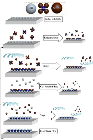
The success of ALD is based on the surface chemistry, since in two stages a layer can be formed after the reaction of two precursors (i.e. reactant and co-reactant) [207] under high vacuum conditions in the order of mTorr. The operation of ALD (Figure 9) is based on four simple steps: precursor (reactant) exposure, precursor purge, co-reactant exposure, co-co-reactant purge.
parameters such as doses times and substrate temperature are controllable via software interface for most ALD systems, operating in a sequence of steps defined by the user (recipes). Therefore, the thickness of the deposited layer is precisely controllable as the film thickness is linearly proportional to the number of ALD cycles completed.
ALD is used to deposit metal oxides such as ZnO, metal nitrides such as TaN, sulfides such as ZnS, and phosphides such as GaP [205]. Each ALD process requires a suitable combination of precursors and co-reactants, which have to be volatile, reactive with each other, and thermally stable in either solid, gas or liquid form [209]. Precursors can be initially classified as reactant (metal) and co-reactant (non-metal), with the co-reactant precursors such as H2O and NH3, being used for depositing oxides and nitrides. The reagents are often inorganic precursors, in which metal atoms are connected to organic ligands groups in order to increase the volatility of the metal at low temperatures. Highly volatile precursors are introduced into the chamber typically using short pulses, while for some involatile precursors it is necessary to bubble gas through the precursor to increase the pickup of vapour into the gas stream.
temperature, but less volatile sources such as tetrakis-ethylmethylamino zirconium precursor, are heated to increase the vapour pressure.
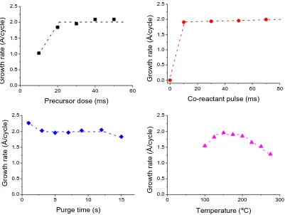
The „ALD window‟ (Figure 10) is shown at the temperature range where the growth rate is fixed (i.e. saturation region). At lower temperatures the reactions cannot occur due to lack of thermal energy, and thus the bonds are not formed (i.e. incomplete reaction) leading to decreased deposition rate. In some cases, condensation may occur at low temperatures leading to an apparent increase in growth rate. If the temperature is higher than the ALD window, the excess thermal energy may induce desorption of the precursor (i.e. break the formed bonds out of the lattice) leading to a reduction in growth rate. Another possibility is the precursor may thermally decompose at high temperatures, leading to CVD-like condensation of growth and hence to an actual increase in growth rate.
Figure 10: Schematic of possible behaviour for the ALD growth per cycle versus temperature [205].
PE-ALD uses plasma as a source of additional energy for reactions that are not feasible with low energy [205]. Hence, plasma can be used at lower growth temperature compared to thermal ALD, which could be particularly useful for temperature sensitive substrates. However, all of the studies mentioned in this report are based on thermal ALD, which could also use low growth temperature and could be more easily used to deposit on high aspect ratio structures.
2.5.1 ZnO deposited by ALD
ALD of ZnO has been extensively studied by many research groups over the last decade [208]-[209],[211]-[217]. Alkyls are the most commonly used precursors for zinc oxide, however, it is reported that these can leave carbon and hydrogen residues [202]. The most commonly used zinc sources are diethylzinc (DEZ) and dimethylzinc (DMZ), with water mostly used as the co-reactant [209], since it allows deposition at temperatures as low as room temperature (i.e. partially crystalline films) [218]. The use of low temperature (90°C) with DEZ allowed deposition of ZnO films on plastic-based polymer solar cells leading to 4.1% power conversion efficiency [211]. DMZ was reported to result in faster growth rate (i.e. up to 3.7 Å/ cycle) than DEZ (i.e. up to 2.1 Å/ cycle) due to shorted ligand of ethyl compared to methyl (i.e. smaller steric hindrance) [212].
higher and lower than the ALD window, the growth rate decreases, due to desorption and incomplete reaction respectively [212]-[213]. The use of DEZ in thermal ALD is reported to result in growth rate of 1.9-2.0 Å/ cycle within the ALD window [215]-[217]. However, when it is used in a PE-ALD the growth rate is higher at 2.8 Å/ cycle due to the high reaction when using oxygen plasma rather than water reactant [217]. The comparison between the two methods also showed higher carrier density for the thermal ALD at low temperatures, while interstitial oxygen sites were formed at low temperature PE-ALD (i.e. <300°C) that acted as electron compensators, making the plasma grown films more suitable for TFT applications [217]. The effect of chamber pressure was also studied and showed that at high pressure of 760 Torr the growth rate increased compared to 2 Torr, attributed to the excess water that remained at the film surface after the water purge step at high pressure, but it is suggested that increased gas velocity can resolve this issue [213].
Similarly to PLD, the increase of zinc interstitials was found to reduce the resistivity [163]
, hence in ALD it was found that at high temperatures the population of those defects increases, leading to higher carrier concentration [219]. The effect of growth temperature on the electrical properties was also studied for low growth temperature at 100°C, which showed low carrier concentration suitable for use in Schottky diodes [220]
. The mobility on the other hand could be increased by increasing film thickness via ALD, as increasing the overall thickness will lead to grain enlargement and hence to the reduction in interfacial and grain boundary scattering [214].
it has the lower surface energy and so grains grow in that direction to minimise the system‟s energy. However, studies also reported films of (10 ̅0) preferred orientation (non-polar) [216],[224]-[227]. In those studies, the growth conditions were different than the standard ALD deposition of ZnO films, including the use of short DEZ doses and short water purge steps [224], the growth at low temperatures (i.e. 150-220°C) [225], and the use of thick films [216],[226]-[227]. The most recent study showing the thickness effect on the grain orientation suggested that the preferred orientation shifted from (0002) to (10 ̅0) direction as the thickness increased [226] (further analysis on the reasons of that change is carried out in chapter 4). Hence, ALD offers the opportunity to set different preferred orientation in ZnO films by changing the film thickness without altering any other growth parameters. A schematic of the crystal structure for both polar and non-polar surface is shown in Figure 11.
Figure 11: Schematic of the top views for polar (c-axis oriented crystals) and non-polar (a-axis oriented crystals) surfaces. The red spheres show zinc atoms and the
Non-polar ZnO films are of interest, in order to avoid electrostatic instability created in the polar surfaces. Polar surfaces lead to spontaneous polarization [228], which creates a non-zero dipole moment that forms macroscopic electric field with perpendicular direction to (0001) plane [229]. This electric charge causes reduction of electron-hole recombination probability and reduces the photons generation [228]. To avoid this effect, non-polar films are more favourable for more efficient optoelectronic devices, such as LEDs and LDs [228],[230]. It was also found important for electrical properties according to Fujimura et al. [231], who stated that ̅ ) oriented films were more conductive compared to ̅ ) and (0001) oriented films. This was also seen by Illy et al., who reported improved photovoltaic performance when the orientation is at ̅ orientation rather than (0002) plane [232].
2.5.2 Doped ZnO deposited by ALD
[image:65.595.113.528.340.517.2]Doping can be easily achieved by ALD using a “delta doping method” (i.e. using one doping cycle in a series of ZnO cycles), such as the one used in this study. As a result, a variety of dopants have been studied using ALD, with focus on producing improved n-type films as shown by some examples in Table 3.
Table 3: List of published doped ZnO films deposited by ALD using different dopants.
Resistivity (Ω·cm)
Carrier density (×1020cm-3)
Carrier mobility (cm2/Vs)
Transp arency Optical gap (eV) Growth T (°C) Film thickness Ref Al
9.7×10⁻⁴ - - >80% - 200 - [242] 3.2×10⁻³ 1.4 14.3 - - 200 45 nm [33] 2.4 ×10⁻³ - - >80% 3.5 150 180 nm [186]
4.4×10⁻³ 1.7 8 92% 3.73 150 100 nm [187] Ga 8.0×10⁻⁴ 1.1 18 - - 300 - [38] Ge 6-7×10⁻³ 2.14 5 >80% 3.62 250 100 nm [27] In 3×10⁻³ 6 20 >85 - 200 180 nm [192] Ti 8.9 ×10⁻⁴ 6.2 10 >80% 3.4 200 100 nm [171] B 6.9×10⁻⁴ ~4 ~20 - - 136 - [247] Hf 6×10⁻⁴ 3.7 20 >80% 3.56 200 200 nm [28] Zr 1.3×10⁻³ 2.2 19.7 92% 3.27 180 100 nm [25]
2.5.3 Zirconium in ALD
Chapter 3
Experimental processes
3.1
Introduction
This chapter addresses the experimental methods used for sample preparation and characterisation. ALD growth is explained in section 3.3, by establishing the growth and sample preparation of all films presented in this thesis. The thickness of these films was then measured by ellipsometry (section 3.2) and confirmed by TEM (section 3.10). TEM was also used to analyse the microstructure of the films, together with XRD (section 3.8) and AFM (section 3.11). The electrical properties of films deposited on glass were characterised using a four-point-probe (part 3.4) and Hall effect measurements (section 3.5), while the chemical state was assessed by XPS (section 3.9). Finally, the optical properties were investigated using photoluminescence (section 3.6) and spectrophotometry (section 3.7).
3.2.
Ellipsometer
and then analyse the reflected elliptically polarised light as shown in Figure 12. The physics behind this technique followed the wave theory of light (Hooke 1660), the polarisation of light theories (Faraday mid 1840s), and the theory of electromagnetic waves (Maxwell 1873) [252]. The development of the first ellipsometer is attributed to Paul Drude (1902). His models are still used today, mostly in spectroscopic ellipsometry, to relate the carrier density with plasma frequency obtained through reflection/transmission as discussed in section 3.7.1.
Figure 12: Schematic of ellipsometer setup.
In ellipsometry two parameters are measured during the scan, the angles Ψ and Δ, which present the light amplitude change and phase change after reflection respectively [252]. From the change in polarisation with ellipse shape (Figure 13), the reflected polarised light consists of two components, the parallel (rp) and the
perpendicular (rs). The numerical components are presented in Equation 1 and
Equation 2, which result in the refractive index (n) calculation in Equation 3.
Polariser Light
source
Analyser
Detector
Sample Linear
polarisation


![Figure 4: Solar spectrum diagram [86].](https://thumb-us.123doks.com/thumbv2/123dok_us/8071184.226964/31.595.148.495.617.708/figure-solar-spectrum-diagram.webp)


![Figure 26: Schematic of the PL experimental setup [267]-[268].](https://thumb-us.123doks.com/thumbv2/123dok_us/8071184.226964/91.595.150.491.291.589/figure-schematic-pl-experimental-setup.webp)
