This is a repository copy of
Effects of rapid thermal annealing on device characteristics of
InGaAs/GaAs quantum dot infrared photodetectors
.
White Rose Research Online URL for this paper:
http://eprints.whiterose.ac.uk/1696/
Article:
Fu, L., Tan, H.H., McKerracher, I. et al. (4 more authors) (2006) Effects of rapid thermal
annealing on device characteristics of InGaAs/GaAs quantum dot infrared photodetectors.
Journal of Applied Physics, 99 (11). 114517-(8 pages). ISSN 1089-7550
https://doi.org/10.1063/1.2202704
eprints@whiterose.ac.uk https://eprints.whiterose.ac.uk/
Reuse See Attached
Takedown
If you consider content in White Rose Research Online to be in breach of UK law, please notify us by
Effects of rapid thermal annealing on device characteristics of InGaAs/ GaAs
quantum dot infrared photodetectors
L. Fu,a兲H. H. Tan, I. McKerracher, J. Wong-Leung, and C. Jagadish
Department of Electronic Materials Engineering, Research School of Physical Sciences and Engineering, The Australian National University, Canberra, Australian Capital Territory 0200, Australia
N. Vukmirović and P. Harrison
School of Electronic and Electrical Engineering, University of Leeds, Leeds LS2 9JT, United Kingdom
共Received 7 November 2005; accepted 17 March 2006; published online 13 June 2006兲
In this work, rapid thermal annealing was performed on InGaAs/ GaAs quantum dot infrared photodetectors 共QDIPs兲 at different temperatures. The photoluminescence showed a blueshifted spectrum in comparison with the as-grown sample when the annealing temperature was higher than 700 ° C, as a result of thermal interdiffusion of the quantum dots 共QDs兲. Correspondingly, the spectral response from the annealed QDIP exhibited a redshift. At the higher annealing temperature of 800 ° C, in addition to the largely redshifted photoresponse peak of 7.4m共compared with the 6.1m of the as-grown QDIP兲, a high energy peak at 5.6m 共220 meV兲 was also observed, leading to a broad spectrum linewidth of 40%. This is due to the large interdiffusion effect which could greatly vary the composition of the QDs and thus increase the relative optical absorption intensity at higher energy. The other important detector characteristics such as dark current, peak responsivity, and detectivity were also measured. It was found that the overall device performance was not affected by low annealing temperature, however, for high annealing temperature, some degradation in device detectivity 共but not responsivity兲 was observed. This is a consequence of increased dark current due to defect formation and increased ground state energy. ©2006 American Institute of Physics.关DOI:10.1063/1.2202704兴
I. INTRODUCTION
With the rapid progress in the growth of self-assembled quantum dots 共QDs兲, their application to high performance optoelectronic devices, such as QD laser diodes and QD infrared photodetectors, have been successfully demon-strated.1–3For developing future optical communication net-works, monolithic integration is a key issue in order to achieve better optical performance, compact size, and low losses. One conventional way of fabricating photonic inte-grated circuits共PICs兲involves repeated etching and regrowth processes, which place a high constraint on the etching and epitaxial growth techniques. In comparison, the approach of postgrowth intermixing 共interdiffusion兲 developed in recent years has offered simple and more practicable schemes for PICs through the modification of the potential profile and thus the optical properties of the quantum-confined hetero-structures. For example, quantum well intermixing 共QWI兲
has been successfully employed to tune the wavelength of quantum well共QW兲lasers4,5and QW infrared photodetectors
共QWIPs兲,6,7 as well as in the fabrication of integrated devices.8 However, due to the large surface area and strain effect, interdiffusion behavior in QDs is much more compli-cated than in QWs. Hence, the technologies that have been developed in QWs cannot be transferred directly to QDs. Although interdiffusion studies have been carried out on
various QD structures using the methods of rapid thermal annealing 共RTA兲,9,10 ion implantation,11,12 and dielectric capping,12,13 few device results have emerged. Midinfrared
共3 – 5m兲 and far-infrared 共8 – 14m兲 photodetectors3,14,15 based on QDs have been predicted to have the advantages of normal incidence and high temperature operation, larger re-sponsivity, and detectivity, in comparison to their QW coun-terpart. However, the operating wavelength of quantum dot infrared photodetectors 共QDIPs兲 is difficult to predict and control accurately due to the extremely sensitive self-organized process of the dot formation. Structure designs such as dots in a well15 have been proposed and demon-strated with flexibilities in altering the operating wavelength of QDIPs by varying the thickness of the quantum well sur-rounding the QDs. However, it still requires highly accurate and reproducible growth conditions. Using the interdiffusion approach, Hwang et al.16 reported the detection wavelength tuning of an InGaAs/ GaAs QDIP after thermal treatment at 700 ° C for 1 min under SiO2capping. A 22 meV redshift of
photocurrent peak was obtained but with a large degradation in device responsivity 共detectivity not reported兲. In this work, a more extensive investigation was carried out to study the postgrowth annealing effects on the intersubband transi-tion of a 15-layer InGaAs/ GaAs QDIP. The device charac-teristics including spectral response, dark current, responsiv-ity, and detectivity were fully investigated and compared after a series of annealing conditions and the implications for the future development of multicolor and broadband photo-detectors are also discussed.
a兲Electronic mail: ful109@rsphysse.anu.edu.au
II. EXPERIMENT
The QDIP structure used in this work was a n-i-n structure17 grown on a semi-insulating GaAs共001兲substrate by metal-organic chemical vapor deposition 共MOCVD兲. Arsine 共AsH3兲, trimethylgallium 共TMGa兲, and trimethyl-indium 共TMIn兲 were used as sources for arsenic, gallium, and indium, respectively. The structure contained 15 layers of 5.7 ML 共monolayer兲 undoped InGaAs 共nominally 50%兲
QDs, separated by 50 nm of GaAs barrier layers and sand-wiched between two highly Si-doped top共300 nm兲and bot-tom共1000 nm兲GaAs contact layers. The growth details have been published in Ref. 18. Rapid thermal annealing was per-formed on the samples at temperatures ranging from 650 to 800 ° C for 30 s under Ar flow. During annealing, the samples were sandwiched between two fresh pieces of GaAs to minimize desorption of As from the surface. Before device fabrication, the samples were examined by cross-sectional transmission electron microscopy 共XTEM兲 using a Philips CM 300 microscope and photoluminescence 共PL兲 using a diode-pumped solid-state frequency-doubled green laser at 532 nm through a 0.5 m monochromator and a cooled In-GaAs photodetector. Then, all of the samples were fabricated into 250⫻250m2 mesa structures using standard photoli-thography, wet chemical etching, and metallization pro-cesses. The 150-m-diameter round top contact and the bot-tom contact were formed by electron-beam evaporation of Ge/ Ni/ Au and alloying at 380 ° C for 60 s. The devices were then mounted in a liquid nitrogen cooled Dewar for further characterization.
III. RESULTS
A. Cross-sectional transmission electron microscopy and photoluminescence
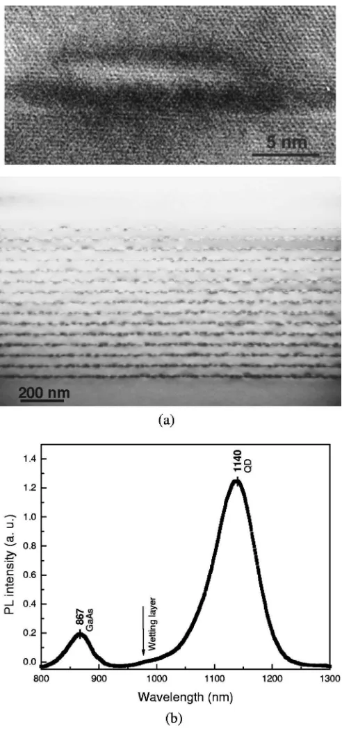
Figure 1共a兲shows the TEM micrographs of the as-grown 15-layer InGaAs/ GaAs QDIPs used in the study. With all 15 QD layers displayed in the structure, no obvious formation of lattice defects such as dislocations can be observed, sug-gesting that good material quality has been maintained after 15-layer dot growth. Figure 1共a兲also shows the high resolu-tion 共HR兲TEM image of a typical QD with a thin wetting layer clearly observed underneath the QD. The QD has a truncated cone shape with ⬃5 nm height and ⬃20 nm base diameter, which agrees well with our atomic force micros-copy measurement.18The HR image also exhibits some con-trast between the middle and outside of the QD, which could have resulted from the nonuniform strain field and/or In dis-tribution in the QDs. The room temperature PL also con-firmed the good quality of the QDIP structure, as shown in Fig. 1共b兲. The main peak of the spectrum was from the dot luminescence and the high energy peak 共⬃867 nm兲 is from the GaAs capping layer/substrate. In addition, a small shoul-der to the main QD peak arising from the wetting layer can also be noted. The high intensity QD peak is located at 1140 nm with the full width at half maximum 共FWHM兲 of 80 meV.
Figure 2 shows the 77 K PL spectra taken from the samples which were annealed from 650 to 800 ° C for 30 s. The QD peak position from the sample annealed at 650 ° C
[image:3.612.314.560.46.572.2]does not show any change compared with that from the as-grown sample. Then, with increasing of the annealing temperature to 700 ° C, the spectrum is blueshifted with a narrowing of the linewidth. The PL energy shift as well as the ratio of the FWHM between the annealed and as-grown samples as a function of annealing temperature are shown in the inset of Fig. 2. It can be seen clearly that with increasing annealing temperature, more intermixing was created, which is consistent with an increase of PL blueshift and a reduction of linewidth. This has been observed previously in FIG. 1.共a兲Bottom: XTEM image of the as-grown 15-layer QDIP structure; top: High resolution XTEM image of a single QD within the 15-layer QDIP structure. 共b兲 Room temperature PL from the as-grown 15-layer QDIP structure.
many studies, as a result of significant thermal inter-diffusion.9,10,13,19However, for our 15-layer QDIP structure, the interdiffusion was initiated at a lower temperature of 700 ° C 关compared with 750 ° C for single and 3-layer QDs
共Ref. 10兲兴, due to a larger accumulated strain. In addition, Fig. 2 also exhibits an enhanced QD luminescence with an-nealing temperature. This is mainly attributed to the spectral narrowing due to the improved QD size homogeneity after interdiffusion as well as the reduction of grown-in defect density around QDs.9,13
B. Detector spectral response
The normal incidence spectral response was measured with a Nicolet Impact 400 Fourier transform infrared共FTIR兲
spectrometer and a SRS 570 low-noise current preamplifier. Figure 3 shows the 77 K spectral response from the device fabricated from the as-grown sample at various positive bi-ases 共on the top contact layer with respect to the bottom contact layer兲. At lower biases, the spectra are very broad and clearly consist of a short wavelength peak at 4.5m
共274 meV兲 and a long wavelength peak at 6.1m
共202 meV兲. With an increase of the bias, the intensity of the 4.5m peak reduces rapidly and the 6.1m peak becomes the dominant peak. To clarify the origin of the two peaks, the spectrum of optical absorption from the ground state was calculated theoretically. Dots in the shape of truncated cones with a base diameter of 20 nm and a height of 5 nm were assumed in accordance with the HR TEM results in Fig. 1共a兲. A wetting layer width of 4 ML and In content of 0.65共larger than the nominal value for growth兲 were assumed. The en-ergy levels and wave functions were calculated using the eight-bandk·pmethod with the strain distribution taken into account via the continuum mechanical model.20In the calcu-lation the dot was embedded in a large cylinder, so that both the wetting layer and the continuum states were discretized that way. The optical absorption cross section on the transi-tion between ground state and any excited state共bound, wet-ting layer, or continuum兲 was calculated as in Ref. 21. Ac-cording to the calculation, the largest optical absorption cross section for x-polarized radiation 共in-plane direction兲 and z-polarized radiation 共growth direction兲 occurs at 42 meV
[image:4.612.51.294.49.219.2]共L1-2兲 and 158 meV 共L1-5兲, respectively, as displayed in Fig. 4. As the states of these energies are below the effective potential barrier共see the schematic of the dot potential in the inset of Fig. 4兲they are localized 共or partially localized兲 to the dot which did not result in detectable photocurrent be-cause the electrons from them have a low escape probability.22Therefore we did not observe any peak related to this transition experimentally. The largest optical absorp-tion cross secabsorp-tion for the bound-to-continuum 共B-C兲 transi-tion under z-polarized light occurs at 202 meV 共L1-6兲 and the next significant transition is at 274 meV共L1-7,⬃10% of the former兲. These two peaks correspond very well with the results from the spectral response measurements. At low bi-ases, although more carriers were excited to the lower energy continuum state共L6兲, many of them could not contribute to photocurrent due to the small electric field. On the other hand, the carriers excited to the higher energy state 共L7兲
travel more easily since they are less likely to be trapped back to the QD energy potentials, thus forming the 4.5m peak共274 meV兲as shown clearly at the bias of 0.3 V in Fig. FIG. 2. The 77 K PL spectra for the QDIP samples annealed at different
temperatures. Inset shows the PL energy shifts 共right兲 and the linewidth
共left兲as a function of annealing temperature.
[image:4.612.242.548.49.220.2]FIG. 3. The spectral response from the as-grown QDIP at various external biases at 77 K.
[image:4.612.49.298.548.728.2]3. With an increase of the bias, the carrier collection effi-ciency is improved much more and most of the carriers cre-ated due to the 202 meV transition can be swept towards the collector, contributing dominantly to the photocurrent at 6.1m.
Figure 5 shows the spectral responses from the QDIPs annealed at different temperatures. The spectra exhibit red-shifted peak wavelengths for the annealing temperatures higher than 650 ° C. The energy and wavelength shifts be-tween the annealed devices and as-grown device are plotted in the inset of Fig. 5. The wavelength redshifting for an-nealed QDIPs is a result of thermal interdiffusion. It is well known23 that interdiffusion of quantum-confined structures
共QWs and QDs兲is able to modify the shape of their potential profiles and thus cause an increase in the interband transition energy 共blueshifted PL兲 and a decrease in that of the inter-subband transition 共redshifted intersubband photocurrent兲. Since the intersubband photocurrent only involves the tran-sitions within conduction band, the energy redshifts obtained in the inset of Fig. 5 are smaller than PL blueshifts in the inset of Fig. 2.
It is interesting to note that for the 800 ° C annealed QDIP, in addition to the large 35 meV energy shift 共or 1.3m wavelength shift兲 obtained from its main peak at 167 meV共7.39m兲 关compared with the 210 meV共6.1m兲
peak of the as-grown sample兴, a second peak at higher en-ergy 共⬃220 meV兲 is clearly displayed in the spectrum, which has not been observed for the other samples. In fact, this high energy peak was detected at all bias conditions from the 800 ° C annealed QDIP and its relative intensity to the low energy 167 meV peak also changed with the bias, as shown in Fig. 6共a兲. Since the 800 ° C RTA introduced the largest degree of interdiffusion, one of its direct effects was the outdiffusion of In from the QD to its surrounding barri-ers, leading to a reduction in the QD In composition and thus a redistribution of the QD energy states and their optical absorption strength. We have approximately modeled these
effects by assuming a smaller In content in the dot of 50%. The calculated absorption spectrum is shown in Fig. 6共b兲, where the two peaks at continuum states共162 and 228 meV兲
show very similar positions to those from the spectral re-sponse of our 800 ° C annealed QDIP. Note that the relative absorption cross section for the high energy peak is increased to 15% of the low energy peak 共10% for the 65% InGaAs QDs兲, which may be a reason for the detection of the high energy peak at all biases. Nevertheless, this is just a simpli-fication of the complicated interdiffusion process. More de-tailed modeling is needed to simulate the intersubband tran-sitions in interdiffused QDs accurately. Due to the presence of two peaks, the 800 ° C annealed QDIP has a broad line-width 共⌬/⬃40%兲, exhibiting a desirable feature for broadband infrared detector applications.
C. Dark current
The dark-current–voltage 共I-V兲 characteristics were measured using a Hewlett-Packard 41408 voltage source at temperatures from 77 to 290 K. Figure 7 shows the bias de-FIG. 5. The spectral responses at 1.2 V from the QDIPs which were
[image:5.612.50.297.47.231.2]fabri-cated from samples annealed at different temperatures. Inset shows the de-vice intersubband transition wavelength shift共right兲as well as the energy shift共left兲as a function of annealing temperature for annealed QDIPs com-pared with the as-grown QDIP.
FIG. 6.共a兲The spectral responses from the 800 ° C annealed QDIP at vari-ous positive biases.共b兲The calculated spectrum of optical absorption cross sections for 50% InGaAs/ GaAs QDs.
[image:5.612.315.560.48.452.2]pendent dark current density for the as-grown QDIP at vari-ous temperatures. Due to the measurement limit, the dark current at low temperatures and small biases cannot be mea-sured accurately 共thus the noisy parts of the curves兲. Also shown in Fig. 7 is the 300 K background photocurrent, indi-cating that the detector is background limited at 77 K for the wide bias range of −2.6 V⬍Vbias⬍3.2 V. The logarithm of
the dark current density versus inverse temperature共1000/T兲
at biases from 0.1 to 1.8 V is shown in Fig. 8. Within the temperature range investigated, each curve shows a consis-tent increase with the temperature, however, the relationship is not linear. Unlike in the case of QWIPs, where thermionic emission is the major source of dark current when tempera-ture is above 77 K, for QDIPs, it has been proposed24 that both field-assisted tunneling and defect-related tunneling
共namely, sequential resonant tunneling or defect-assisted tun-neling兲contribute to the dark current. Consequently, two dif-ferent regions can be distinguished from the temperature de-pendent curves. The high temperature region共⬎125 K兲was ascribed to the thermally limited region共through thermionic emission and field-assisted tunneling兲, and the low tempera-ture region 共⬍125 K兲 to a defect-limited region. From Fig. 8, this transition behavior can also be identified in all the curves at around 125 K, suggesting that the dark current may arise from different sources. Indeed, since the GaAs barriers of our QDIP structure were grown at a low temperature of 550 ° C 共650 ° C is normally used to obtain good quality GaAs兲 to ensure the quality of dot formation, defects are inevitably formed which could result in additional tunneling path for dark current at low temperature. By fitting the linear section of the high temperature region 共⬎125 K兲 of the curves using the Arrhenius relation, the activation energyEa is estimated and shows a decrease as a function of bias, as plotted in the inset of Fig. 8.
The 77 K I-V characteristics for annealed QDIPs are plotted in Fig. 9共a兲. Annealing causes an increase in the dark current of the devices. Compared with as-grown device, the
dark current was increased by one order of magnitude after 650 and 700 ° C annealings whereas 800 ° C annealing in-creased the dark current by about two orders of magnitude. The temperature dependent dark current density at 0.3 V for these samples is plotted in Fig. 9共b兲. The annealed samples display more nonlinear characteristics than the as-grown sample, indicating that their dark currents originated from more temperature-invariant components. We ascribe it to the defects that are generated in the GaAs barriers and at QD interfaces during the high temperature annealing. Normally, annealing is considered to be an effective method to remove defects from the semiconductor structures. However, for a highly strained structure, such as in QDs, it may lead to the formation of extended defects. It has been found by XTEM
[image:6.612.322.559.47.237.2]共Ref. 25兲that annealing at 700 ° C of a 30-layer InAs/ GaAs QDIP 共where some defect centers have already been ob-served in the as-grown sample兲lead to the formation of ex-tended defects due to strain relaxation and dopant-related defect complexes due to high doping in the contact layers. Therefore, up to four orders of magnitude increase of dark current and severely degraded device performance have been observed. For our 15-layer QDIP, although XTEM and PL measurements clearly revealed the good quality of the as-grown QD layers, extended and dopant-related defects may still form during annealing, leading to the increase of dark current. Nevertheless, these defects may be of smaller size and lower concentration in our annealed QDIPs, which have not significantly affected the PL intensity as observed in Fig. 2. High temperature annealing 共at 800 ° C兲 apparently had much stronger effect on increasing the dark current than the low temperature annealing共at 650 and 700 ° C兲. On the other hand, both PL and spectral response results indicate that in-terdiffusion for our 15-layer QDIPs initiates from 700 ° C. It resulted in an increase of ground state energy level and thus a reduction of thermal activation energy of dark current. Therefore, compared with the 650 ° C annealed and as-grown samples, the slope of the dark current density versus FIG. 7. TheI-Vcharacteristics for the as-grown QDIP measured at different
[image:6.612.52.299.48.259.2]temperatures. The 300 K background photocurrent measured at 77 K is also shown.
temperature curve was increasingly reduced for the 700 and 800 ° C annealed samples due to interdiffusion. However, the similar amount of dark current obtained for both 650 and 700 ° C annealed samples again stresses the important con-tribution from the defect-related component.
D. Responsivity and detectivity
The blackbody response photocurrentIph and spectrum
of noise current in for our QDIPs were measured simulta-neously using a low-noise current preamplifier 共SRS 570兲
and a fast Fourier transform spectrum analyzer共SRS 760兲. A germanium block was placed in front of the aperture of the blackbody source to filter out near-IR radiation from the blackbody.3 The signal was measured at a modulation fre-quency of 140 Hz and the absolute peak responsivityRpwas
calibrated with an IR-301 blackbody source at 800 ° C. Fig-ure 10共a兲shows the peak spectral responsivity versus bias for all of the QDIP samples fabricated in this study. For the as-grown QDIP, with increase of positive bias, the responsiv-ity increased from 0.065 mA/ W at 0.1 V to 26 mA/ W at 2 V. For the negative bias, the responsivity is enhanced from 0.041 mA/ W at −0.1 V to 61.8 mA/ W at −2 V. The slightly asymmetric shape of the curve between forward and reverse biases could be due to the intrinsically asymmetric nature of QDs. Different from the results in Ref. 16 where the responsivity was largely decreased after thermal treat-ment, the responsivity of the annealed devices does not show much variation from the as-grown sample, with a marginal improvement at low annealing temperatures. However, the peak responsivity is relatively low and this could be ex-plained by two reasons. Firstly, due to the undoped active region and a large number of QD layers, the supply of car-FIG. 9. 共a兲The 77 KI-Vcharacteristics for the annealed QDIPs compared
[image:7.612.53.302.49.506.2]with the as-grown QDIP.共b兲The dark current density versus inverse tem-perature 共1000/T兲 for the annealed QDIPs compared with the as-grown QDIP at 0.3 V.
FIG. 10. 共a兲The bias dependence of peak responsivity for the annealed QDIPs compared with the as-grown QDIP.共b兲The bias dependence of peak detectivity for the annealed QDIPs compared with the as-grown QDIP.
[image:7.612.300.558.49.500.2]riers from our QDIP structure through background doping and/or contact layers may not be sufficient to occupy most of the QD states. Secondly, due to the shape of our QDs, which are wide in the in-plane direction 共⬃20 nm兲 and narrow in the growth direction 共⬃5 nm兲 as a result of the self-assembled growth process, as mentioned earlier, strong con-finement has been achieved only in the growth direction. Consequently, the B-C transition that dominates the photo-current was generated from thez-polarized light.22However, due to the near-normal incidence geometry used in our mea-surement, only a small amount ofz-polarized light was pro-duced共from the extrinsic light scattering26兲, resulting in the low responsivity in our samples.
The specific peak detectivity was calculated by D*=R
p
冑
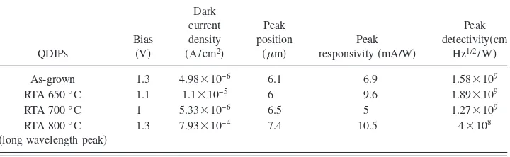
Adet⌬f/in, where Adetis the detector area, in is the noise current, and⌬f is the bandwidth. Figure 10共b兲shows the peak detectivity versus bias curves measured at 77 K. Similar peak detectivities were obtained for the as-grown, and 650 and 700 ° C annealed QDIPs, whereas annealing at 800 ° C caused an obvious reduction of detectivity. Table I summarizes the overall detector performance at 77 K for all the QDIP samples studied in this work, including the dark current density, the peak detection wavelength, the maximum peak detectivity, as well as the corresponding peak respon-sivity. It can be noted that the device performances have been well maintained at low annealing temperatures. For the higher annealing temperature of 800 ° C, the detector detec-tivity was reduced; however, the responsivity was not de-graded. This could be ascribed to combined effects from in-creased ground state energy 共more photocurrent and dark current兲 and more defect formation 共more dark current兲. Nevertheless, the degradation of device properties observed in this study is much less in extent compared with other reported studies under similar conditions,16,25which is attrib-uted to the good growth quality of the QDIP structure. By optimizing the structure design, doping, and other parameters of MOCVD growth, the device performance is expected to be further improved and degradation from thermal annealing can also be minimized. These results are encouraging for the future implementation of multicolor detectors using inter-mixing techniques such as dielectric capping or ion implan-tation. It has been shown12 that in comparison with QWs, large differential wavelength shifts can be achieved in QD structures at low annealing temperatures by low-dose ion im-plantation or dielectric capping. During these processes only a low density of point defects will be created to induce in-terdiffusion, which may not cause too much degradation tothe device performance. On the other hand, the largely broadened spectrum with two detection peaks obtained by simple annealing at higher temperature is also a desirable feature for broadband imaging applications.
IV. CONCLUSIONS
The rapid thermal annealing effects on the main device properties of a 15-layer InGaAs/ GaAs quantum dot infrared photodetector have been investigated. Compared with the de-vice fabricated from the as-grown structure, low annealing temperatures did not cause much change of the device per-formance. A higher annealing temperature produced a large wavelength shift 共up to 1.3m兲 and although there was some degradation on the detector’s peak detectivity, this was relatively small and can be further minimized by improving the QDIP structure design and growth quality. These results suggest that by utilizing intermixing techniques, multicolor or broadband QDIPs can be developed in the future without compromising too much the device performance.
ACKNOWLEDGMENTS
The authors would like to thank M. Aggett, T. Halstead, and D. Gibson for their continuous technical assistance. The financial support from Australian Research Council is also acknowledged.
1
Nano-Optoelectronics, Concepts, Physics and Devices, edited by M. Grundmann共Springer, Berlin, 2002兲.
2
K. Kamath, P. Bhattacharya, T. Sosnowski, T. Norris, and J. Phillips, Elec-tron. Lett. 32, 1374共1996兲.
3
A. D. Stiff, S. Krishna, P. Bhattacharya, and S. W. Kennerly, IEEE J. Quantum Electron. 37, 1412共2001兲.
4
H. H. Tan and C. Jagadish, Appl. Phys. Lett. 71, 2680共1997兲.
5
L. Fu, H. H. Tan, M. B. Johnston, M. Gal, and C. Jagadish, J. Appl. Phys.
85, 6786共1999兲.
6
M. B. Johnstonet al., Appl. Phys. Lett. 75, 923共1999兲.
7
L. Fu, H. H. Tan, C. Jagadish, N. Li, N. Li, X. Q. Liu, W. Lu, and S. C. Shen, Appl. Phys. Lett. 78, 10共2001兲.
8
M. Buda, J. Hay, H. H. Tan, L. Fu, C. Jagadish, P. Reece, and M. Gal, J. Electrochem. Soc. 150, G481共2003兲.
9
R. Leon, Y. Kim, C. Jagadish, M. Gal, J. Zou, and D. J. H. Cockayne, Appl. Phys. Lett. 69, 1888共1996兲.
10
P. Lever, L. Fu, H. H. Tan, C. Jagadish, P. Reece, and M. Gal, in Third IEEE Conference on Nanotechnology, San Francisco, CA, 2003 共IEEE Publishing Co., Piscataway, NJ, 2003兲, p. 852.
11
P. Lever, H. H. Tan, C. Jagadish, P. Reece, and M. Gal, Appl. Phys. Lett.
82, 2053共2003兲.
12
L. Fu, P. Lever, H. H. Tan, C. Jagadish, P. Reece, and M. Gal, IEE Proc.: Circuits Devices Syst. 152, 491共2005兲.
13
P. Lever, H. H. Tan, and C. Jagadish, J. Appl. Phys. 96, 7544共2004兲.
14
[image:8.612.126.486.66.177.2]D. Pan, E. Towe, and S. Kennerly, Appl. Phys. Lett. 73, 1937共1998兲.
TABLE I. Summary of device properties for all the QDIPs studied in this work.
QDIPs
Bias
共V兲
Dark current density
共A / cm2兲
Peak position
共m兲
Peak responsivity共mA/W兲
Peak detectivity共cm
Hz1/2/ W兲
As-grown 1.3 4.98⫻10−6 6.1 6.9 1.58⫻109
RTA 650 ° C 1.1 1.1⫻10−5 6 9.6 1.89⫻109
RTA 700 ° C 1 5.33⫻10−6 6.5 5 1.27⫻109
RTA 800 ° C
共long wavelength peak兲
15
S. Krishna, S. Raghavan, G. v. Winckel, P. Rotella, A. Stintz, C. P. Morath, D. Le, and S. W. Kennerly, Appl. Phys. Lett. 82, 2574共2003兲.
16
S. H. Hwang, J. C. Shin, J. D. Song, W. J. Choi, J. I. Lee, and H. Han, Microelectron. J. 36, 203共2005兲.
17
Z. H. Chen, O. Baklenov, E. T. Kim, I. Mukhametzhanov, J. Tie, A. Madhukar, Z. Ye, and J. C. Campbell, J. Appl. Phys. 89, 4558共2001兲.
18
L. Fu, P. Lever, K. Sears, H. H. Tan, and C. Jagadish, IEEE Electron Device Lett. 26, 628共2005兲.
19
L. Fu, P. Lever, H. H. Tan, C. Jagadish, P. Reece, and M. Gal, Appl. Phys. Lett. 82, 2613共2003兲.
20
O. Stier, M. Grundmann, and D. Bimberg, Phys. Rev. B 59, 5688共1999兲.
21
N. Vukmirović, Z. Ikonić, V. D. Jovanović, D. Indjin, and P. Harrison,
IEEE J. Quantum Electron. 41, 1361共2005兲.
22
H. C. Liu, Opto-Electron. Rev. 11, 1共2003兲.
23
Semiconductor Quantum Wells Intermixing, edited by E. H. Li共Gordon and Breach, Amsterdam, 2000兲.
24
A. D. Stiff-Roberts, X. H. Su, S. Chakrabarti, and P. Bhattacharya, IEEE Photonics Technol. Lett. 16, 867共2004兲.
25
K. Stewart, M. Buda, J. Wong-Leung, L. Fu, C. Jagadish, A. Stiff-Roberts, and P. Bhattacharya, J. Appl. Phys. 94, 5283共2003兲.
26
H. C. Liu, M. Buchanan, and Z. R. Wasilewski, inInternational Workshop on Intersubband Transitions in Quantum Wells: Physics and Devices, ed-ited by S. S. Li and Y. K. Su共Kluwer Academic, Taiwan, 1998兲, p. 50.