This is a repository copy of Electromagnetic coupling to an enclosure via a wire
penetration.
White Rose Research Online URL for this paper:
http://eprints.whiterose.ac.uk/97223/
Version: Accepted Version
Proceedings Paper:
Thomas, D.W.P., Denton, A., Benson, T.M. et al. (6 more authors) (2001) Electromagnetic
coupling to an enclosure via a wire penetration. In: Electromagnetic Compatibility, 2001.
EMC. 2001 IEEE International Symposium on. , pp. 189-188.
https://doi.org/10.1109/ISEMC.2001.950588
[email protected]
https://eprints.whiterose.ac.uk/
Reuse
["licenses_typename_other" not defined]
Takedown
If you consider content in White Rose Research Online to be in breach of UK law, please notify us by
ELECTROMAGNETIC COUPLING
TO AN ENCLOSURE VIA
A
WIRE PENETRATION
D W P Thomas,
A
Denton,
C
Christopoulos,
The University of Nottingham, University Park,Nottingham, UK.
T M Benson,
J
Paul
T Konefal,
J F Dawson,
A
C Marvin,
S
J Porter
The University of York,
York,UK
Abstract:
This paper presents an efficient model, which can be computed in seconds, for the coupling of external electromagnetic fields to the contents of an enclosure via wire penetrations. The coupling path accounts for the coupling of an external electric field to a wire penetration that establishes an internal electric field via the connect and internal wire segment. The internal electric field then couples onto another victim wire segment, inside the box. The accuracy of the model is demonstrated by the good agreement obtained between predicted induced voltage on the victim wire segment, and experimental measurements.Introduction
An important mechanism for the coupling of electromagnetic fields to the interior of an enclosure is through wire penetrations. This paper presents an efficient and accurate model for this type of coupling. An external electromagnetic field induces a current onto an external wire which penetrates an enclosure via a connector. The current on the internal segment of the wire penetration will then excite an internal electromagnetic field in the form of propagating and evanescent waveguide modes within the enclosure. The internal electromagnetic fields can also induce currents on other structures within the enclosure and in this work another wire segment, or monopole is considered.
In the model described, the wire penetrations are represented as monopoles. Equivalent circuits for these monopoles, external source and a transmission line representation of the enclosure waveguide modes are used to represent the complete coupling path. It is generally accepted [1,2] that the method of moments (MOM) [3] gives accurate results for the impedance of dipole or monopole antennas. We have, therefore, used an empirical approximation for the monopole equivalent circuit impedance and effective length (hence antenna factor). This approximation is derived from the analysis of a number of MOM simulations and is similar to that proposed in [4, 51. This equivalent circuit for the monopole is then incorporated into an equivalent circuit model of the coupling of the electromagnetic fields to the wire penetrations and for the excitation of the enclosure internal electromagnetic fields [ 6 ] .
Theory
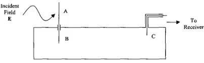
The problem studied is as depicted in Fig. 1.
In Fig.
1 an
external field impinges o n a n external wire (monopole A) protruding from a cuboidal box. The wire passes through aBNC
connector t oa
second
shorter wire (monopoleB)
inside the box. The secondwire
excites electromagnetic fields within the box and these are sensed b y a third wire(monopole C). The signal picked u p b y wire C is passed t o
a
receiver (network analyser) via a 50Q coaxial cable where the receivedpower
is measured. In the analysis ofthis experiment antenna models of the
wires are produced
and a model for the electromagnetic coupling of the wires within thebox are developed.
I
I B
I CI
[image:2.613.329.531.297.360.2]I I
Figure 1 Experimental arrangement studied
Wire radiators
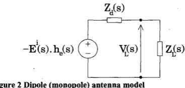
Wire radiators affect EMC by emitting and absorbing radiation in the same way as monopole/dipole antennas. Thus to describe a wire radiator in circuit solutions of EMC problems, the antenna- like properties of the wire are represented by an equivalent circuit in combination with an effective length function. To enable an efficient computational solution of the circuit model, the frequency-dependent impedance and effective length functions arc approximated using simple expressions. As described in [4], the variation of a dipole’s input impedance over a wide frequency range can be modelled as an equivalent circuit containing frequency dependent lumped elements. Further research along these lines by [5] identified the four element circuit model used in this paper. To the authors’ knowledge, an approximation to the frequency-dependent effective length function has not previously appeared in the literature. Fig. 2 shows the model of a dipole (monopole) antenna: Using s to represent the complex frequency,
E‘(’) is the component of the incident electric field polarised in the direction of the antenna, k,(s) is the frequency-dependent effective length function, Z&) is the self impedance, ZL(s) is the load impedance and the voltage developed across the load is
VL6).
From Fig. 2, the antenna factor is
Thus the calculation of the voltage VL(s) across a known load requires knowledge of both the self-impedance Z&) and the effective length function h,(s).
I
Figure 2 Dipole (monopole) antenna model
{
Fig. 3 shows the geometry and the four-element circuit model of the self impedance of a dipole developed by [5]: The tip-to-tip length is 2h and the diameter is 2a. The equivalent circuit consists of the electrostatic capacitance CO in series with a parallel combination of C,, LI and RI.
The circuit model of the dipole yields
1
S-
1 Cl
z d
=-+
1 1 (Q) (2)sco
,2+,-+-ClRl 4 C l
I
:
h
+TIRl
1
Zd(a)= Rr(a)+jXd(0)I
As shown in Fig. 3, by putting s=jwj2nj (2) has the
form
Zd ( f ) = R,. ( f )
+
j x d (f) where R,fl is the radiation resistance and Xdfl is the dipole reactance. This is then fitted to the self impedance obtained using MOM. The low frequency fitting pointis chosen as the half-wave resonant frequency f o = % h , where
R,
( f o ) = Ro = 72Cl and x d ( f o ) = 0 . The high frequency pointis selected as the full-wave resonance frequency fl = % h ,
where R, (fl) = R1 the first maximum value of the radiation resistance. The expressions we have derived differ from [5] because their goal was to approximate the low frequency impedance accurately, whereas we have constructed a model which approximates the self-impedance up to the full-wave resonant frequency. The empirical coefficients are then (with empirical values in the square brackets)
( M W (3)
[l. 15 l]ln(h / a )
+
[64.7 11 hf o =
WHz) (4)
[8.401]in(h/ a)
+
[87.67] hA =
(PF) (5)
[27.88]h
c -
-
ln(h/a)-[1.452]Z,, = [70.88](ln(h/~)-[0.7648]) (Cl) (6) Z,, = [125.2](ln(h/a)-[1.768])
(a)
(7)Up to the full wave resonant frequencyfi the effective length may be approximated using
h o z
(10)
he(s) =
s2
+
s26h+
where it is found that the effective length resonant frequency fh = mh/2n is
[7.609]1nK)+ [92.57]
h (MH4 (11) f h =
and the damping frequency is
where
[image:3.612.319.550.92.310.2](he(- = h(0.7063]lnk)+[0.1387]) (m) (13)
Fig. 4 compares the self-impedance of a typical dipole obtained using MOM with the equivalent circuit model and Fig. 5 compares the effective length of a typical dipole obtained using MOM with the values given by (3).
1500
-
E
'0 10002
m
m 500
m
$a, 0
(I)
-500
. .innn ."__
0 50 100 150 200 250 300 350 400 450 500
[image:3.612.68.289.246.421.2]Frequency (MHz)
Figure
4Self-impedance of a dipole antenna
(2h=0.8189m,
2a=3.0mm).
0
-0.5
1
-1.5
0 50 100 150 200 250 300 350 400 450 500
[image:3.612.320.551.347.645.2]Frequency (MHz)
Figure
5 Effective length of a dipole antenna
(2h=0.8189m, 2a=3.0mm).
Electric dipole coupling to waveguide
Inside a metallic enclosure a wire penetration will excite electromagnetic fields as waveguide modes. Consider a short current carrying wire element AB (electric dipole) which is placed inside the waveguide in the near constant plane z=z,, of any orientation, and let the waveguide be short circuited at z=O and
z=-d. Using the transmission line analogy, the schematic equivalent circuit for a particular mode n is as in Fig. 6. A voltage on the transmission line will induce a current on the dipole. Likewise, a voltage on the dipole will induce a current in the transmission line. The principle of reciprocity dictates that the magnitude of these effects are the same, so that we can model the interaction by a mutual capacitance C where
Idip = jwcvWG (14)
IWG = jwcVdip (15)
In (14) and (15) the currents, voltages and capacitance are all considered to act in the plane z=z,, the location of the dipole or wire element. This is a reasonable assumption if the dipole is short or if it is oriented in the x-y plane. Considering the electric fields of a mode n (TE or TM) produced by the forward voltage
5'"
and reverse voltage V:" on the transmission line,S.C.
VWG
S.C.
Zz;
= j c ~ C ( ~ ) V $ i ( z ~ ) (17)Assuming that in the absence of a cavity the wire element or dipole carries a current IsoUrce, the dipole currents from each mode combine with I,,,,, to produce a total current on the dipole of
n=l
The back current source in transmission line k (see Fig. 5 ) is then given by
I;&
= jo&k)ZintITo, (19)In this way, a single voltage on one transmission line will induce a voltage in every other transmission line, and the modes are properly coupled. The electric dipole itself is characterised by
Isouxe, and Z i n p
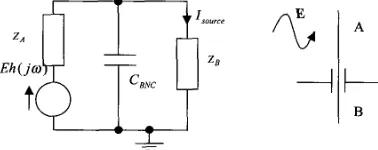
The arrangement for the receiving wire penetration has an equivalent circuit comprising of two monopoles, one external (monopole A) with self-impedance Z, and one internal (monopole B) with self impedance Z, , as shown in Fig 7. The capacitance for the BNC connector can be found from standard equations [7] and was calculated to be 1.39 pF. This is used to derive the
source current as from rearranging (1) we have
The complete input circuit for the internal section of wire penetration is then as given in Fig. 8. The voltage source in Fig. 7 is replaced by the current source I,,,, (20) in series with the self- impedance Z,. This then is coupled to a current source I+
representing the coupling of the internal fields to the wire (monopole B).
Plane of constant or near constant z
Figure 6. Schematic equivalent circuit for electric coupling of current element to waveguide, indicating the role of the mutual Capacitance C.
we can write the induced current on the dipole as
(16) 1
= -
jI
E(") .dlZint
where
E(")
is the combined electric field produced by both forward and reverse voltages of mode n. The voltage reflection coefficient V:'") /bo""
is equal to -1 for a short circuit at z=O.Since the forward and reverse components of E(") depend linearly
on
5"")
and V,"'") respectively, both of these terms can beeliminated from (16), enabling the mutual capacitance C") to be calculated. Details of this calculation are shown in [9]. Zin, is the self-impedance of the wire element given by ( 2 ) .
Wire to waveguide mode coupling
Consider the first N lowest order modes, each with its own mutual capacitance
cc"
to the electric dipole, located in the plane z=zc(n=I
....N.
For a transmission line voltage in mode n of VWG'")(z),the induced current in the dipole is
A
I-
B
Figure 7. Equivalent circuit for wire penetration as two
[image:4.612.67.277.327.424.2]monopoles joined through
a
metal plat viaa
BNC socket [image:4.612.326.515.418.493.2] [image:4.612.323.476.539.654.2]Multimode wire to wire coupling
The equivalent circuit of Fig. 8 may be extended to include two wires, and to take into account several modes of propagation. Figure 9 illustrates the resulting equivalent circuit, where for simplicity only two modes are shown, the TElo and TE20 modes. There are eight nodes in Fig. 9, labelled 1, li, 2, 2i, A l ,
A2,
B1 and B2. The pair of dependent current sources labelled Iwgsl and ZdjpB] effect the mutual coupling of the source wire (monopole B) to the waveguide via the TElo mode (14) and (15). Similarly, coupling of the victim wire (monopole C) to the waveguide via the TE10 mode is achieved by Iwcl and IdjpC]. The source wire (monopole B) couples to the TE20 mode by means of current sources IwB! and IdrpB2, whilst I,, and Idipc2 provide the required TE2o couplmg for the victim wire (monopole C). Note the mechanism by which mode coupling takes place between the TElo and TEz0 modes. currents such as IdjpB] and flow through a common impedance of ZB in series with the parallel combinationZA and the connector capacitance CBNc, inducing a voltage ZBZTo, across the wire monopole impedance ZB. This voltage then induces currents on both the TElo and TEz0 analogous transmission lines, via the current sources IwBl and
IwgB2.
The latter two current sources are the circuit implementations of (1 9)with k referring to the TElo and TEZ0 modes respectively.
The circuit may easily be extended to include higher order modes. For each additional mode n, an extra analogous transmission line is added to the circuit (with its associated current sources and impedances), similar to the two transmission lines illustrated in Fig. 9. Two extra current sources, one across I d @ and the other across IdjpC, are also added to the circuit for every additional mode considered. These extra current sources provide the coupling of the voltage on the analogous transmission line for mode n to the source and victim wires illustrated in Fig. 9, as prescribed by (17). They are linearly dependent on the mutual capacitances CB@) and
CC") between the analogous transmission line and the source and
victim wires respectively. The process of current combination described by (1 8) takes place on both the input and output circuits of Fig. 8, while completion of the mode coupling process described by (19) is effected by current sources such as IwBl and
Iwcl which are strapped across the analogous transmission lines. Once again, IwBl and IwcI are linearly dependent on Cs(") and
c,",
respectively.The mutual capacitance for waveguide mode mn for the source wire (monopole B) can be derived from (1 6) and can be reduced to
The victim wire is loaded by the 50!2 cable impedance. The mutual capacitance of the victim wire (monopole C) for waveguide mode mn, found from (1 6), and can be reduced to where the waveguide width is a and terms s and transverse wave impedance Z,, are defined in the appendix.
I
I
Figure 8. Equivalent circuit for wire to wire coupling inside an enclosure
For each transmission line, current sources P , H and impedances
Z,, represent the Norton equivalent circuit of the section of transmission line between the two wire monopoles. For example, for the TElo analogous transmission line of Fig. 8, we have
9
= T 2 v ~ 1+
T l v ~ 2 and H i = TlVA1 + T ~ V A ~ where 1and T, = -(1- coth(y,,h)). Here h is 1
TI =
=lo siWy10h) z10
the distance along the waveguide propagation axis between the two monopoles. This form of dependency for P and H is particularly useful for nodal analysis of the circuit. Z,, and Z,,
represent the impedances of the short circuited sections of transmission line between the wires and the two ends of the box. For example, ZS2 = Z20 tanh(yzoZ) where I is the distance of the source wire from the plane z=-d. Z,, is taken as the transverse wave impedance of the mode [ 81.
[image:5.612.328.528.97.318.2]Equation 22 reflects directly the fact that the voltage across the 50Q cable impedance is hidden from view as far as the waveguide is concerned. In (21), when the voltage VA2 is positive, the
voltage
Vzi
is negative. Hence the additive sign in this equationto eliminate the effect of the 'hidden' voltage across the 5OQ resistance in the output circuit of Fig. 8. The remaining coupling capacitances and current sources are treated in a similar fashion for all the other modes considered. This complication arises in the theory simply because the wires cannot be totally isolated from the waveguide walls.
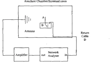
EXPERIMENTAL MEASUREMENTS
Antenna
The full experimental arrangement inside the screened room and inside the anechoic chamber is as shown if Fig. 9. In the screened room a Log-periodic antenna was used and in the anechoic chamber a Bilog antenna was used. The external wire was 8cm long and the internal wires B and C were 5cm and 2.1 cm respectively. All wires are 0.8mm diameter and located along the centre line of the box (x=uL'). The initial box was of dimensions 29.2cm x29.2cmxl1.5cm. Below 700 MHz all the waveguide modes are evanescent. Between 700 MHz and lGHz only the TElo mode propagates. Also, since the source and victim wires are located along the box centre line, the TElo is the dominant excited mode. The measurement results for the experiments performed in the screened room and anechoic chamber are shown in Fig. 10 and 11 compared with the theoretical results considering only the TElo mode. The results show good agreement above 500 MHz. Below 500 MHz the results are
masked by the noise level of the amplifier. The differences between Figs. 10 and 1 1 are due to the different antennas used and the different output powers of the amplifiers.
Return
Simulated sZ1 magnitude usrng TEIO mode only
ZW 300 4W 5W 600 700 800 900 IMQ
Frequency (MHz)
Figure 10. Experimental results from the screened room compared with the theoretical results.
Anechoic ChamberiScreened room
-lw 2w I 3W 4W SW 6W 703 8W 9M IWO I
F q v e n c y (MHz)
[image:6.612.321.532.82.650.2]Only the TElo mode was considered in the theoretical results of Fig. 10 and 11. The experiments of Fig. 10 and 11 were repeated using a larger box of dimensions 60cmx50cmx3cm. This larger box supported several propagating mode below IGHz. The source and victim wires were also located off centre so that several modes were excited other than the TElo mode. In this case wire A wise identical to the earlier experiments while wires B and
C consisted of wire sections of length 5cm and diameter Imm. In this case the TE and TM modes up to and including m = 4 and
n=4, is compared with the experimental results. The results are shown in fig. 12 and it again gives very good agreement between theory and experiment. Below 300 MHz the results are masked by the noise level of the amplifier. I
[image:6.612.327.530.101.247.2]Figure 11. Experimental results from the anechoic chamber compared with the theoretical results.
Figure 9. Experimental arrangement in the screened room and anechoic chamber
m
Figure 12 Experimental and theoretical results for the lager box in the anechoic chamber
CONCLUSIONS
[image:6.612.96.280.419.526.2]wire impedances and the coupling path. The results show excellent agreement with the experimental results carried out in
two separate environments and two different box sizes.
REFERENCES
[ l ] M J Salter and M J Alexander. EMC antenna calibration and the design of an open field site. Measurement Science and Technology, 2510-519, 1991.
[2] S F Kawako and M Kanda. Effective length and input impedance of NIST standard dipoles. IEEE Transactions on Electromagnetic Compatibility, 39(4):404-408, November 1997.
[3] R F Harrington. Field computation by moment methods. Macmillan,
NY,
1962.[4] G W Streable and L W Pearson. A numerical study on realizable broad-band and equivalent admittances for dipole and loop antennas. IEEE Transactions on anteenas and propagation, 29(5):707-717, September 1981.
[5] T G Tang, Q M Tieng and M W Gunn. Equivalent circuit of a dipole antenna using frequency-independent lumped elements. IEEE Transactions on Antennas and Propagation, 41 (1): 100- 103, January 1993.
[6] T Konefal, J F Dawson, A Denton, S J Porter, A C Marvin, T M Benson, C Christopoulos and D W P Thomas, Electromagnetic field predictions inside screened enclosures containing radiators EMC York 1999, IEE Pub. 464, July 1999, pp 95-100.
[7] Sander, K.F. and Reed,G.A.L., Transmission and propagation of electromagnetic waves, 2* edition, Cambridge University Press, 1986.
[8] Collin, R.E., 'Field theory of guided waves,' 2nd edition, IEEE Press, New York, 1991.
Acknowledgements
The authors wish to thank EPSRC (Research grants GRL-89723 and GR/L-89716), BAe BASE, Matra BAe Dynamics, ALSTOM Research and Technology Centre and Zuken-Redac for their support during this project.
APPENDIX 1
1
(W
P,
= - j r (P,
real and positive when w>
0, ) (A4)pT =-1 (A71