cavity QED
Thesis by Paul Edward Barclay
In Partial Fulfillment of the Requirements for the Degree of
Doctor of Philosophy
California Institute of Technology Pasadena, California
2007
c
2007
Acknowledgments
Since my first visit to Caltech, Oskar Painter has been exceedingly generous with his time, energy, and insight. Oskar’s enthusiasm for the work of his students, his curiosity, and his desire to deeply understand whatever he is working on has never ceased to be inspiring, and I feel fortunate to have learned so much about all aspects of research from him.
I have also been fortunate to interact with Hideo Mabuchi, with whom meetings always ended with fresh ideas and optimism. Hideo’s combination of creativity and perspective is something I hope to be able to replicate.
In my experience, the greatest strength of Caltech is its students. In Kartik Srinivasan, with whom I have shared an office since arriving in Pasadena, one couldn’t ask for a better colleague. Matthew Borselli never ceased being helpful. Thomas Johnson could always be counted on to do things precisely. Building up the lab with this trio was a great experience, and I’m sure that its future will be bright in the hands Raviv Perahia, Jessie Rosenberg, Chris Michael, and Matt Eichenfeld. In the atomic physics lab, I was lucky to work closely with Benjamin Lev. Ben always generously treated his hard work as if it were ours. With help from Michael Armen, John Stockton, Andrew Berglund, Kevin McHale, and everyone else in Mabuchi-lab, Joe Kerckhoff and I have had an exciting time catching up on Ben’s considerable knowledge after he graduated, and I am grateful for Joe’s dedication.
Two people from my time at the University of British Columbia have had a lasting influence. For two summers, Garry Clarke gave me the best job that I’m likely to ever have, and in the process convinced me to go to graduate school. Jeff Young showed me how much fun doing physics can be. I am ever thankful for their continued support and advice.
in Pasadena earlier.
Abstract
The sub-wavelength optical confinement and low optical loss of nanophotonic devices dra-matically enhances the interaction between light and matter within these structures. When nanophotonic devices are combined with an efficient optical coupling channel, nonlinear optical behavior can be observed at low power levels in weakly-nonlinear materials. In a similar vein, when resonant atomic systems interact with nanophotonic devices, atom-photon coupling effects can be observed at a single quanta level. Crucially, the chip based nature of nanophotonics provides a scalable platform from which to study these effects.
This thesis addresses the use of nanophotonic devices in nonlinear and quantum optics, including device design, optical coupling, fabrication and testing, modeling, and integration with more complex systems. We present a fiber taper coupling technique that allows effi-cient power transfer from an optical fiber into a photonic crystal waveguide. Greater than 97% power transfer into a silicon photonic crystal waveguide is demonstrated. This optical channel is then connected to a high-Q(>4×10⁴), ultra-small mode volume (V <(λ/n)3) photonic crystal cavity, into which we couple>44% of the photons input to a fiber. This permits the observation of optical bistability in silicon for sub-mW input powers at telecom-munication wavelengths.
To port this technology to cavity QED experiments at near-visible wavelengths, we also study silicon nitride microdisk cavities at wavelengths near 852 nm, and observe resonances withQ >3×10⁶ andV <15 (λ/n)3. ThisQ/V ratio is sufficiently high to reach the strong coupling regime with cesium atoms. We then permanently align and mount a fiber taper within the near-field an array of microdisks, and integrate this device with an atom chip, creating an “atom-cavity chip” which can magnetically trap laser cooled atoms above the microcavity. Calculations of the microcavity single atom sensitivity as a function of Q/V
Contents
Acknowledgments v
Abstract vii
List of figures xxi
List of tables xxii
Glossary of Acronyms xxiii
Publications xxv
1 Introduction 1
1.1 Microcavities . . . 2
1.2 Fiber optic coupling at the nanoscale . . . 3
1.3 Organization . . . 3
2 Interfacing photonic crystal waveguides with fiber tapers: design 5 2.1 Coupled-mode theory . . . 7
2.2 k-space design . . . 12
2.3 Contradirectional coupling in a square lattice PC . . . 16
2.4 Supermode calculations . . . 21
2.5 Conclusion . . . 24
3 Efficient fiber to cavity coupling: theory and design 25 3.1 Efficient and ideal waveguide-cavity loading . . . 26
3.2 Mode-matched cavity-waveguide design . . . 28
4 Probing photonic crystals with fiber tapers: experiment 34
4.1 Experimental details . . . 35
4.1.1 Fiber taper fabrication . . . 36
4.1.2 Fiber probing measurement apparatus . . . 37
4.1.3 Photonic crystal fabrication . . . 38
4.2 Efficiently coupling into photonic crystal waveguides . . . 41
4.3 Real- and k-space waveguide probing . . . 45
4.3.1 Bandstructure mapping . . . 46
4.3.2 Real-space mapping . . . 49
4.4 Efficient coupling into PC microcavities . . . 50
4.5 Conclusion . . . 56
5 Nonlinear optics in silicon photonic crystal cavities 57 5.1 Modeling nonlinear absorption and dispersion in a microcavity . . . 58
5.1.1 Nonlinear absorption . . . 58
5.1.2 Nonlinear and thermal dispersion . . . 62
5.2 Nonlinear measurements . . . 66
5.3 Conclusion . . . 72
6 Silicon nitride microdisk resonators 73 6.1 SiNx Microdisk fabrication . . . 74
6.2 Microdisk mode simulations . . . 76
6.2.1 High Q modes of 9 μm diameter microdisks at 852 nm . . . 78
6.2.2 Scaling of Qrad and V with microdisk diameter . . . 80
6.3 Microdisk testing using a fiber taper . . . 82
6.3.1 Waveguide microdisk coupling . . . 82
6.3.2 Microdisk testing at 852 nm . . . 84
6.3.3 Comparison with PECVD microdisks . . . 86
6.4 Resonance wavelength positioning . . . 87
6.5 Multidisk arrays . . . 88
6.6 Predicted microdisk cavity QED parameters . . . 90
6.6.1 Cavity QED with Cs atoms . . . 92
6.6.3 Practical limitations . . . 94
6.7 Conclusion . . . 96
7 An atom-cavity chip 97 7.1 Fiber coupled microcavities for atom chips . . . 98
7.1.1 Robust fiber mounting . . . 98
7.1.2 Installation in a UHV chamber . . . 102
7.2 Microcavity surface sensitivity to Cs vapor . . . 103
7.3 Atom trapping on the atom-cavity chip . . . 107
7.3.1 Atom chip basics . . . 107
7.3.2 Integrating cavities with atom chips . . . 110
7.4 Conclusions and outlook . . . 114
8 Microcavity single atom detection 116 8.1 Atom induced modification of fiber coupled cavity response . . . 118
8.1.1 Single mode cavity . . . 118
8.1.2 Whispering gallery mode cavity . . . 123
8.1.3 Simulations . . . 128
8.2 Single atom detection: signal to noise . . . 132
8.2.1 Signal to noise ratio . . . 133
8.2.2 Photon detection schemes . . . 135
8.2.3 Simulations . . . 138
8.3 Summary . . . 142
A Bloch modes and coupled mode theory 144 A.1 Formulating Maxwell’s equations . . . 144
A.1.1 Orthogonality of Bloch modes . . . 146
A.1.2 Additional properties of Bloch modes . . . 148
A.2 Coupled mode equations: Lorentz reciprocity method . . . 152
A.2.1 Coupling between two periodic waveguides . . . 155
A.2.2 Power conservation . . . 157
B.2 Field normalization . . . 161 B.3 Coupling efficiency . . . 162
List of Figures
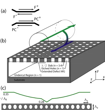
2.1 (a) Schematic of the coupling scheme, showing the four mode basis used in the coupled mode theory. (b) Coupling geometry. In the case considered here, the coupling is contra-directional. (c) Grading of the hole radius used to form the waveguide, and a top view of the graded-defect compressed-lattice (Λx/Λz = 0.8) waveguide unit cell. . . 6
2.2 Approximate bandstructure of fundamental even (TE-like) modes for a square lattice PC of air holes with radiusr/Λ = 0.35 in a slab of thicknessd= 0.75Λ and dielectric constant= 11.56. Calculated using an effective index ofneffTE= 2.64, which corresponds to the propagation constant of the fundamental TE mode of the untextured slab. The inset shows the first Brillouin-zone of a rectangular lattice. . . 13
2.3 Projection of the square lattice bandstructure onto the first Brillouin-zone of a line defect with the same periodicity of the lattice and oriented in the
X1 → Γ direction. Bandedges whose modes have dominant wavenumbers in
theX1→Γ direction (i.e. k=kˆz) are drawn with solid black lines. Bandedges
whose modes have dominant wavenumbers in the X2 → M direction (i.e.
k=kzˆz+π/Λxˆx) are drawn with dashed black lines. . . . 14
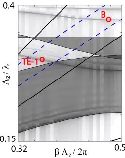
2.5 3D FDTD calculated bandstructure for the waveguide shown in Fig. 2.1(c). The dark shaded regions indicate continuums of unbound modes. The dashed lines are the dispersion of fiber tapers with radius r = 0.8Λz = 1Λx (upper line) and r = 1.5Λz = 1.875Λx (lower line). The solid black lines are the air (upper line) and fiber (lower line) light lines. The energies and wavenumbers of modes TE1 and B are ˜ωΛz/2π = 0.304 and 0.373 at βΛz/2π = 0.350 and 0.438 respectively. . . 17
2.6 Mode TE1field profiles calculated using FDTD. Dominant magnetic field
com-ponent (a) |By(x, y = 0, z)|; and (b) |By(x, y, z = 0)|; (c) Dominant electric field component transverse Fourier transform|E˜x(kx, y= 0, z)|. Note that the dominant transverse Fourier components are near kx = 0. . . 18
2.7 (a) Power coupled to PC mode TE1from a tapered fiber with radiusr = 1.15Λx
placed with a d= Λx gap above the PC as a function of detuning from phase matching and coupler length. (b) Power coupled at ω=ω0 to the forward and
backward propagating PC and fiber modes as a function of coupler length. . 19
2.8 Mode B field profiles calculated using FDTD. Dominant magnetic field com-ponent (a) |By(x, y = 0, z)|, (b) |By(x, y, z = 0)|. (c) Dominant electric field component transverse Fourier transform |E˜x(kx, y = 0, z)|. Note that the dominant transverse Fourier components are near kx =±π/Λx. . . 20
2.9 Power coupled to PC mode B from a tapered fiber with radius r = 1.55Λx placed with a d= Λx gap above the PC as a function of detuning from phase matching and coupler length. . . 22
2.10 (a) FDTD calculated bandstructure of the full fiber taper photonic crystal system. The fiber taper has a radius r = 1.17Λz = 1.46Λx, and is d = Λz = 1.25Λx above the PC waveguide. The TE1-like and fiber-like dispersion
3.1 (a) Schematic of the fiber taper to PC cavity coupling scheme. The blue arrow represents the input light, some of which is coupled contradirectionally into the PC waveguide. The green arrow represents the light reflected by the PC cavity and recollected in the backwards propagating fiber mode. The red colored region represents the cavity mode and its radiation pattern. (b) Illustration of the fiber-PC cavity coupling process. The dashed line represents the “local” band-edge frequency of the photonic crystal along the waveguide axis. The step discontinuity in the bandedge at the PC waveguide - PC cavity interface is due to a jump in the longitudinal (ˆz) lattice constant. The parabolic “potential” is a result of the longitudinal grade in hole radius of the PC cavity. The bandwidth of the waveguide is represented by the gray shaded area. Coupling between the cavity mode of interest (frequencyω0) and the mode matched PC
waveguide mode (ωWG =ω0) is represented by γ0e, coupling to radiating PC
waveguide modes is represented byγj>e 0, and intrinsic cavity loss is represented by γi. . . 26
3.2 (a,b) High-Q defect cavity mode profiles. Plots of the magnetic field pattern are shown in (a) the x−z plane (|By(x, y = 0, z)|), and (b) the x−y plane (|By(x, y, z = 0)|). (c,d) PC waveguide TE1 mode field profiles, taken in the
(a) the x−z plane and (b) the x−y plane. . . 30
3.3 Coupling from the defect cavity to the PC waveguide for varying waveguide lattice compression at instances in time when the cavity magnetic field is a minimum (left) and a maximum (right). The envelope modulating the waveg-uide field is a standing wave caused by interference with reflections from the boundary of the computational domain. The diagonal radiation pattern of the cavity is due to coupling to the square lattice M points, and is sufficiently small to ensure a cavity Q of ≈ 105. |B| for (a) ΛWG
4.1 Schematic of the coupling scheme. (a) Illustration of the fiber taper in the “U-mount” configuration that is employed during taper probing of the PC chip. (b) Illustration of the fiber taper positioned in the near field of the PC waveguide, and the contra-directional coupling between waveguide that occurs on-resonance. . . 35
4.2 Illustration of the optical path within the fiber optic measurement apparatus. DT and DR represent photodetectors used to measure the transmitted and
reflected signals respectively. . . 38
4.3 SEM image of a fabricated photonic crystal array. One of the devices is posi-tioned below a fiber taper. Also visible is the edge of the “isolation” mesa on which the PC array is defined. . . 40
4.4 (a) Waveguide geometry and finite-difference time-domain (FDTD) calculated magnetic field profile (By) of the TE1 mode. (b) SEM image of the high (r1)
reflectivity waveguide termination. The PC waveguide has a transverse lattice constant Λx = 415 nm, a longitudinal lattice constant Λz = 536 nm, and length L = 200Λz. (c) Dispersion of the PC waveguide mode, and the band edges of the mirror termination for momentum along the waveguide axis (ˆz). The shaded region is the reflection bandwidth of the mirror. . . 42
4.5 (a) Reflection and (b) transmission of the fiber taper as a function of wave-length for a taper height of 0.20μm. Both signals were normalized to the taper transmission with the PC waveguide absent. (c) Measured taper transmission minimum, reflection maximum, and off-resonant transmission as a function of taper height. Also shown are fits to the data, and the resulting predicted coupler efficiency, |κ|2. . . 45
4.6 (a) Approximate bandstructure of the PC waveguide studied in Sec. 4.3. Only the TE-like modes that couple most strongly with the fiber taper are shown. The dispersion of a typical fiber taper is also indicated. (b) FDTD calculated magnetic field profile for the TE1mode, taken in the mid-plane of the dielectric
4.7 3D FDTD calculated dispersion of the TE1 (dotted line), TE2 (dashed line),
and TM1 (dot-dashed line) modes for the (a) un-thinned (tg = 340 nm), and
(b) thinned (tg = 300 nm) graded lattice PC waveguide membrane structure
(nSi = 3.4). Measured transmission through the fiber taper as a function of
wavelength and position along the tapered fiber for (c) un-thinned sample and (d) thinned sample (different tapers were used for the thinned and un-thinned samples, so the transmission versus lc data cannot be compared directly).
Transmission minimum (phase-matched point) for each mode in the (e) un-thinned and (f) un-thinned sample as a function of propagation constant. In (a-b), the lightly shaded regions correspond to the tuning range of the laser source used. . . 48
4.8 Coupling characteristics from the fundamental fiber taper mode to the TE1
PC waveguide mode of the thinned sample (tg = 300 nm). Transmission versus wavelength for (a) 1.9μm and (b) 1.0 μm diameter taper coupling regions for varying taper-PC waveguide gap,g. Transmission in (a,b) has been normalized to the transmission through the fiber-taper in absence of the PC waveguide. . 49
4.9 Coupling characteristics from the fundamental fiber taper mode to the TE1
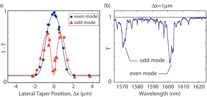
PC waveguide mode of the thinned sample (tg = 300 nm). (a) 1−Tminversus
lateral position (Δx) of the 1.0μm diameter fiber taper relative to the center of the PC waveguide (g = 400 nm). (b) Transmission versus wavelength for Δx ∼ 1 μm. Transmission in (a-b) has been normalized to the transmission through the fiber-taper in absence of the PC waveguide. . . 50
4.10 SEM image of an integrated PC waveguide-PC cavity sample. The PC cavity and PC waveguide have lattice constants Λ ∼ 430 nm, Λx ∼ 430 nm, and Λz ∼550 nm. The surrounding silicon material has been removed to form a diagonal trench and an isolated mesa structure to enable fiber taper probing. 51
4.11 (a) Illustration of the device and fiber taper orientation for (i) efficient PC waveguide mediated taper probing of the cavity, and (ii) direct taper probing of the cavity. (b) Normalized depth of the transmission resonance (ΔT) at
4.12 (a) Measured reflected taper signal as a function of input wavelength (taper diameter d∼1 μm, taper heightg= 0.80 μm). The sharp dip at λ∼1589.7 nm, highlighted in panel (b), corresponds to coupling to the A02 cavity mode. (c) Maximum reflected signal (slightly detuned from the A02 resonance line), and resonance reflection contrast as a function of taper height. The dashed line at ΔR = 0.6 shows the PC waveguide-cavity drop efficiency, which is independent of the fiber taper position forg≥0.8 μm. . . 54
5.1 (a) Measured cavity response as a function of input wavelength, for varying PC waveguide power (taper diameter d∼1μm, taper height g= 0.80 μm). . 67
5.2 (a) Power dropped (Pd) into the cavity as a function of power in the PC waveguide (Pi). The dashed line shows the expected result in absence of nonlinear cavity loss. (b) Resonance wavelength shift as a function of internal cavity energy. Solid blue lines in both Figs. show simulated results. . . 68
5.3 (a) Simulated effective quality factors for the different PC cavity loss channels as a function of power dropped into the cavity. (b) Contributions from the modeled dispersive processes to the PC cavity resonance wavelength shift as a function of power dropped into the cavity. (Simulation parameters: ηlin∼0.40,
ΓthdT /dPabs = 27 K/mW,τ−1 ∼0.0067+(1.4×10⁻⁷)N0.94whereN has units
of cm−3 and τ has units of ns.) . . . 70
5.4 Dependence of free-carrier lifetime on free-carrier density (red dots) as found by fitting Δλo(Pi) and Pd(Pi) with the constant material and modal param-eter values of Table 5.1, and for effective PC cavity thermal resistance of ΓthdT /dPabs = 27 K/mW and linear absorption fraction ηlin = 0.40. The
solid blue line corresponds to a smooth curve fit to the point-by-point least-squared fit data given byτ−1∼0.0067 + (1.4×10⁻⁷)N0.94, whereN is in units of cm−3 and τ is in ns. . . 71
6.2 Electric field magnitude distribution of the four highestQrad modes with
res-onance wavelengths near 852 nm for a 9 μm diameter, 250 nm thick SiNx microdisk with a 45 degree sidewall profile. The calculated radiation quality factor Qrad, optical mode volume Vo (assuming a standing wave mode), and normalized peak exterior energy density η are also indicated for each mode. . 77
6.3 Resonance wavelength andQradof the lowest radial order (highestmandQrad)
modes with resonance wavelengths near 852 nm for a 9 μm diameter, 250 nm thick SiNx microdisk with a 45 degree sidewall profile. . . 79
6.4 FEM calculated Vo and Qrad of the p = 1 TE and TM modes as a function
of microdisk diameter, for h = 250 nm. (a) Qrad at λ = 852 nm. (b) Vo at λ = 852 nm. (c) Qrad at λ = 637 nm. (d) Vo at λ = 637 nm. In all of the mode volume calculations, it was assumed that the microdisk supports standing wave modes. . . 81
6.5 (a) Schematic of fiber taper coupling to a microdisk traveling wave mode. (b) Generalization of the coupling process depicted in (a) to represent a microdisk that supports standing wave modes. s and t are the input and output field amplitudes of the fiber taper field, respectively (see Ch. 8). . . 82
6.6 Taper transmission when the taper is aligned close the perimeter of a 9 μm diameter microdisk. This wide wavelength scan was obtained by performing a DC motor sweep of the laser diode grating position. This data shows a typical “family” of microdisk modes. The high frequency noise on the off-resonance background is due to etalon effects in the laser. . . 84
6.7 Fiber taper transmission when the taper is positioned in the near field of a 9μm diameter microdisk, for two fiber taper positions. The data in (a), (b), and (c) are for different nominally identical microdisks fabricated simultaneously on the same chip. The red lines are fits using a model that includes coupling between the microdisk and the tapers, as well as between traveling wave modes of the microdisk. . . 85
6.9 (a) Optical microscope image of part of an array of 10 microdisks, aligned with a fiber taper. (b) Transmission spectra of the fiber taper when it is aligned with an array of 10 microdisks. . . 89 6.10 Cavity QED parameters for a Cs atom in the microdisk near field, as a function
of microdisk diameter. The Cs atom is taken to be at the field maximum outside of the microdisk. The microdisk thickness is h = 250 nm, and λ ∼
852 nm. In calculating κ, Q = min4×106, Qrad
. (a,b) Interaction and decoherence rates for the fundamental (a) TE mode, (b) TM mode. (c) Strong-coupling parameter. (d) Bad cavity parameter. . . 93 6.11 Cavity QED parameters for an diamond NV center interacting with the
mi-crodisk near field, as a function of mimi-crodisk diameter. The NV center is taken to be at the field maximum outside of the microdisk. The microdisk thickness is h = 250 nm, and λ ∼ 637 nm. In calculating κ, Q = min4×106, Qrad
. (a,b) Interaction and decoherence rates for the fundamental (a) TE mode, (b) TM mode. (c) Strong coupling parameter. (d) Bad cavity parameter. . . 95
7.1 Illustration of a fiber taper mounted in a “U” configuration to a glass slide. The fiber taper is bonded to the glass slide using UV curable epoxy. . . 99 7.2 (a) Illustration of a fiber coupled photonic chip integrated with an atom chip.
(b) SEM image of a fiber taper permanently mounted to a microdisk using epoxy microjoints. . . 100 7.3 Resonance wavelength shift of the 9μm diameter SiNxmicrodisk studied in Ch.
6 as a function of time exposed to Cs. The Cs partial pressure was 10−9−10−8 Torr. . . 104 7.4 Simulated accumulated Cs film thickness as a function of time for varying
background pressure. For the upper curve, at the time indicated by the dashed vertical line the Cs partial pressure is reduced by an order of magnitude. . . 106 7.5 (a) Illustration of a magnetic trap formed by superimposing a homogeneous
7.6 Illustration of the laser beam and microwire geometry used to form the atom chip mirror-MOT. During the MOT formation, current flows through the “u” section of the “h” microwire circuit. . . 109
7.7 Illustration of the laser beam and microwire geometry used to form a mirror-MOT when the cavity-mirror is integrated with the atom chip. (a) Top view, (b) end view, (c) side view. The zoomed-in detail (d) shows how a MOT can be formed above an array of cavities on an otherwise uniform mirror. The shadow from the cavities only extends above the surface as high as the cavity footprint. . . 111
7.8 SEM images of a cavity-mirror chip. The mesa contains a 3×10 array of 9
μm diameter microdisks, and is isolated by ∼ 20 μm above the surrounding gold coated Si substrate. . . 112
7.9 Photoluminescence images of laser cooled atoms being delivered to the micro-cavity array on the atom chip. The red-colored area highlights the position of the cavity array. The atom-cavity chip is oriented as in Fig. 7.7(b). Each im-age is taken by halting the experiment at the specified time after the transfer from the the macro mirror-MOT to the cavity has begun, zeroing the magnetic fields, and exciting the atoms using the MOT beams. The resulting photo-luminescence, as well as light scattered by the atom chip surface, is imaged using a zoom lens, and is collected by a CCD camera. . . 113
8.1 Depiction of microdisk atom detection experiment. . . 117
8.3 Same simulations as in Fig. 8.3, but including a degenerate whispering gallery mode (|β| = 0). Also shown is the reflected waveguide signal. Both fully-quantum and semiclassical solutions were used, as indicated. For the spectra on the right, the semiclassical and fully-quantum results can not be differenti-ated by eye. The power dependent calculations in (a) were limited to Pi < Ps for computational reasons. . . 131 8.4 Same simulations as in Fig. 8.3, but with microcavity induced coupling
be-tween the degenerate whispering gallery modes (|β|/2π = 9 [GHz], β real). The atomic dipole is detuned by −|β| from the uncoupled cavity resonance frequency, so that is spectrally aligned with the lower frequency standing wave mode. Although γe is unchanged from the simulation results in Figs. 8.3 and 8.2, in the standing wave basis K → K = K/(K + 1) = 0.34. Also shown is the reflected waveguide signal. The semiclassical and fully-quantum results cannot be differentiated by eye. . . 132 8.5 Calculated SNR for a fiber coupled single mode (left) and degenerate
whis-pering gallery mode (right) microcavity with g/2π = 1 GHz and (a) Q= 106, (b) Q = 105, (c) Q = 104. In all of the calculations, λo = 852 nm, γa/2π = 0.005 GHz, Δωa = Δωc = 0, K = 0.52 (Te,o = 0.1). The various detector parameters are given in Table 8.1. The power dependent calculation in (a) was limited to Pi< Ps for computational reasons. . . 141 8.6 Calculated SNR for fiber coupled single mode microcavities with g/2π =
10 GHz and (a)Q= 105, (b)Q= 104. In all of the calculations,λo= 852 nm,
List of Tables
5.1 Nonlinear optical coefficients for the Si photonic crystal microcavity. . . 69
Glossary of acronyms
APD Avalanche photodiode.
cQED Cavity quantum electrodynamics.
CCDCharge coupled detector.
CW Continuous wave.
e-beam Electron beam.
FCA Free carrier absorption.
FCD Free carrier dispersion.
FDTD Finite difference time domain.
FEM Finite element method.
FEMLAB Finite element method software package distributed by Comsol.
FSR Free spectral range.
HD Heterodyne.
ICP-RIEInductively coupled reactive ion etch.
MOT Magneto-optical trap.
LIAD Light induced atom desorption.
LPCVD Low pressure chemical vapor deposition.
SEMScanning electron microscope.
SOISilicon on insulator.
SPCMSingle photon counting module.
TETransverse electric.
TM Transverse magnetic.
TPATwo photon absorption.
NV Nitrogen vacancy.
PC Photonic crystal.
PCWG Photonic crystal waveguide.
PECVDPlasma enhanced chemical vapor deposition.
PMMAPolymethyl methacrylate.
RPMRevolutions per minute.
Q Quality factor.
QED Quantum electrodynamics.
UV Ultra-violet.
UHV Ultra high vacuum.
Publications
• P. E. Barclay, K. Srinivasan, M. Borselli, and O. Painter. Experimental demonstration of evanescent coupling from optical fibre tapers to photonic crystal waveguides. IEE Elec. Lett., 39(11) 842–844, 2003.
• K. Srinivasan, P. E. Barclay, O. Painter, J. Chen, A. X. Cho, and C. Gmachl.
Exper-imental demonstration of a high quality factor photonic crystal microcavity. Appl. Phys. Lett., 83(10) 1915–1917, 2003.
• O. Painter, K. Srinivasan, and P. E. Barclay. Wannier-like equation for the resonant
cavity modes of locally perturbed photonic crystals. Phys. Rev. B, 68(3) 035214, 2003.
• P. E. Barclay, K. Srinivasan, and O. Painter. Design of photonic crystal waveguides for evanescent coupling to optical fiber tapers and integration with high-Q cavities.
J. Opt. Soc. Am. B, 20(11) 2274–2284, 2003.
• P. E. Barclay, K. Srinivasan, M. Borselli, and O. Painter. Efficient input and output
optical fiber coupling to a photonic crystal waveguide. Opt. Lett., 29(7) 697–699, 2004.
• B. Lev, K. Srinivasan, P. E. Barclay, O. Painter, and H. Mabuchi. Feasibility of
detecting single atoms using photonic bandgap cavities. Nanotechnology, 15 S556– S561, 2004.
• S. A. Maier, P. E. Barclay, T. J. Johnson, M. D. Friedman, and O. Painter. Low-loss fiber accessible plasmon waveguide for planar energy guiding and sensing. Appl. Phys. Lett., 84(20) 3990–3992, 2004.
and spatial properties of planar photonic crystal waveguide modes via highly efficient coupling from optical fiber tapers. Appl. Phys. Lett., 85(1) 4–6, 2004.
• K. Srinivasan, P. E Barclay, and O. Painter. Fabrication-tolerant high quality factor
photonic crystal microcavities. Opt. Expr., 12(7) 1458–1463, 2004.
• K. Srinivasan, P. E. Barclay, M. Borselli, and O. Painter. Optical-fiber based mea-surement of an ultra-small volume high-Q photonic crystal microcavity. Phys. Rev. B, 70 081306(R), 2004.
• M. Borselli, K. Srinivasan, P. E. Barclay, and O. Painter. Rayleigh scattering, mode
coupling, and optical loss in silicon microdisks. Appl. Phys. Lett., 85(17) 3693–3695, 2004.
• P. E. Barclay, K. Srinivasan, and O. Painter. Nonlinear response of silicon photonic
crystal microresonators excited via an integrated waveguide and a fiber taper. Opt. Expr., 13 801–820, 2005.
• K. Srinivasan, P. E. Barclay, M. Borselli, and O. Painter. An Optical-Fiber-Based
Probe for Photonic Crystal Microcavities. IEEE JSAC, 23 1321–1329, 2005.
• S. A. Maier, M. D. Friedman, P. E. Barclay, and O. Painter. Experimental demon-stration of fiber-accessible metal nanoparticle plasmon waveguides for planar energy guiding and sensing. Appl. Phys. Lett., 86(7) 071103, 2005.
• K. Srinivasan, M. Borselli, T. J. Johnson, P. E. Barclay, O. Painter, A. Stintz, and S. Krishna. Optical loss and lasing characteristics of high-quality-factor AlGaAs microdisk resonators with embedded quantum dots. Appl. Phys. Lett., 86 151106, 2005.
• P. E. Barclay, B. Lev, K. Srinivasan, H. Mabuchi, and O. Painter. Integration of
Chapter 1
Introduction
From afar, fabrication of nanoscale optical components can appear to be predominantly mo-tivated by the same forces that have driven developments in the microelectronics industry, where we have become accustomed to equating smaller with more powerful. Unsurpris-ingly, to a large degree this intuition is correct. Optical chips containing dense arrays of devices have the potential for high bandwidth data processing, and already play a role in the telecommunications industry [1, 2, 3]. However, as a scientist, the motivation for minitur-ization can come from elsewhere: the desire to study optical effects that cannot be observed easily, if at all, without the help of wavelength scale confinement of light. Reassuringly, these two views of optical miniturization are not in conflict. Instead, these interests drive each other: Novel chip-scale optical phenomena often find applications in practical devices, and the usefulness of a scalable, integrated optical platform is not lost on physicists wanting to study increasingly complex systems.
1.1
Microcavities
Optical microcavities [7] confine light to wavelength scale volumes for relatively long times, and are the cornerstone of nanophotonics. At resonant frequencies, they enhance the local electromagnetic energy density, and support extremely large field strengths for low input powers. Generally speaking, the high quality factor (Q) and small mode volume (V) of microcavities make them sensitive to intensive and extensive properties, respectively, of their host environment. For example, a high-Q cavity can be extremely sensitive to small changes in the bulk susceptibility of its environment, while a smallV cavity can be sensitive to local changes.
While microcavities can be fabricated from a wide range of geometries, including pho-tonic crystal [8, 9, 10, 11, 12] and whispering gallery mode [13, 14, 15, 16, 17] resonators, any given microcavity can be characterized by Q and V. These quantities are defined in terms of the local field supported by the microcavity. For a microcavity resonance excited by a single photon, the field maxima Emax inside the cavity is simply written as
Emax=
ω
2V , (1.1)
where ω is the optical frequency of the resonance, and is the dielectric constant of the microcavity at the field maximum. To maintain this field strength in steady state, it is necessary to replenish the microcavity with new photons at the same rate at which they leak out due to imperfections or limitations in the microcavity design. This decay rate is related to Q:
dN dt =−
ω
QN, (1.2)
where N is the number of photons stored in the cavity at a given time t. From energy conservation, this indicates that the power required to storeN photons in the cavity scales as 1/Q. Using the above two equations, for a given power dropped into a cavity, the peak intracavity energy density can be shown to scale with Q/V.
all-optical switching [24, 25, 26] has been observed. LargeQ/V is also essential for experiments in cavity QED [4, 5, 6], which study the coherent energy exchange between single photons and single atoms [27, 28, 29] or quantum dots [30, 31, 32, 33]. Within the cavity, the atom-photon interaction rate and atom-photon dissipation rate scale with 1/V1/2and 1/Q, respectively, and when the atom-photon interaction rate is sufficiently strong compared to the photon and atomic decoherence rates, the coupled atom-cavity system can be used in applications such as single photon generation [34, 35, 36, 37] and quantum state transfer [38, 39] for quantum information processing.
1.2
Fiber optic coupling at the nanoscale
In addition to requiring large field enhancements and photon lifetimes, any useful application of microcavities in nonlinear and quantum optics demands an efficient optical interface between the microcavity and external optics. The mismatch in both spatial dimensions and refractive index between wavelength-scale photonics and conventional fiber optics is severe, and without engineering a transition between the macro- and the nano-scale, the loss of optical fidelity is extremely high.
Fiber tapers [40, 41] are versatile tools that make this transition adiabatically. They have been used to efficiently excite resonances in whispering gallery mode cavities [42, 43, 15, 44, 45], and as discussed in this thesis, photonic crystal waveguides [46, 47, 48] and microcavities [11]. The highly integrated nature of chip based photonics also comes to our aid, as microcavities can be efficiently sourced from on-chip waveguides [25, 49] that are in turn coupled to the outside world. Using these tools to establish efficient optical channels between the laboratory and nanophotonic devices, the next challenge is to integrate fiber coupled devices with more complex experimental systems, such as those used in neutral atom based cavity QED experiments.
1.3
Organization
into practice in Ch. 4, where we demonstrate nearly perfect coupling at telecommunication wavelengths between a fiber taper and a Si photonic crystal waveguide, and use the taper to probe the dispersive and spatial properties of the bound photonic crystal waveguide modes. Efficient coupling between the photonic crystal waveguide and a high-Q, ultra-small V
photonic crystal microcavity is also demonstrated. The nonlinear optical properties of this Si microcavity are studied in Ch. 5, where optical bistability is observed at sub-mW input powers.
Chapter 2
Interfacing photonic crystal waveguides
with fiber tapers: design
The utility of photonic crystal (PC) devices relies heavily upon one’s ability to efficiently couple light into and out of them. At the outset of the work contained in this thesis, no efficient technique had been demonstrated for efficiently exciting guided modes of planar photonic crystal waveguide structures. Initial photonic crystal waveguide experiments [52, 53] relied upon end-fire coupling between single mode fibers and the cleaved facet of a PC waveguide, and exbited extremely small coupling efficiency (<20 dB) because of the extreme spatial and refractive index mismatch between subwavelength high-index PC structures and optical fibers.
A number of methods for overcoming this problem have been studied. Perhaps the most obvious approach is to use adiabatic transitions [54, 55, 56] from “standard” ridge waveguides to source PC waveguides. However, coupling from fibers into high refractive index ridge waveguides poses similar problems, and requires the use of on-chip spot-size converters [57, 49, 58, 53] for high efficiency. Other groups have developed free-space grating assisted coupling techniques [59, 60] that utilize the periodicity of the photonic crystal waveguide to scatter light at near-normal incidence into bound photonic crystal waveguide modes, with modest efficiency.
Undercut Region (n = 1)
λ / 2 Slab (n = 3.4) Substrate
Extended Defect WG Etched Holes (n = 1)
(c)
(b)
z x
y
Λx
Λz
0.35
0.28
r / Λz
F
PC
PC
F
++
[image:32.612.117.460.88.445.2]-(a)
Figure 2.1: (a) Schematic of the coupling scheme, showing the four mode basis used in the coupled mode theory. (b) Coupling geometry. In the case considered here, the coupling is contra-directional. (c) Grading of the hole radius used to form the waveguide, and a top view of the graded-defect compressed-lattice (Λx/Λz= 0.8) waveguide unit cell.
scale probe” for testing of multiple devices on a planar chip.
Evanescent coupling
between waveguides. Full power transfer requires that, in addition, no other radiation or guided modes of either waveguide participate in the coupling, either due to a large phase mismatch and/or weak transverse overlap. Fiber taper coupling has been shown to be extremely valuable in this regard (in comparison to simple prism coupling, which involves a continuum of modes), and was first used to provide near perfect single mode coupling to dielectric microsphere [61, 42, 62] and toroid [14] resonators for ultra sensitive measurement of high-Q whispering gallery modes. In a similar manner, fiber taper probes can be used to couple to two dimensional PC membrane waveguides, thanks to their undercut air-bridge structure that suppresses radiation from the fiber into the substrate, and their zone-folded dispersion that enables phase matching between the dissimilar fiber and PC modes. Thus, by designing a PC waveguide whose defect mode has a transverse field profile that sufficiently overlaps the fiber taper’s, efficient power transfer between the waveguides can be achieved. Furthermore, the flexibility in lattice engineering afforded by PCs allows this waveguide to be designed to couple efficiently to PC defect cavities, providing a fiber-PC waveguide-PC cavity optical probe.
In the remainder of this chapter, closely following Ref. [63], we discuss the design of a PC waveguide that satisfies the requirements outlined above. In Sec. 2.1, a simple coupled mode theory that models coupling between a fiber taper and a PC is presented, and the desired waveguide properties are illuminated mathematically and discussed in more detail. In Sec. 2.2, a generalk-space analysis of bulk PC bandstructures is used to determine which types of defect modes have the desired properties. The results from these sections are then applied to the design and analysis of a PC waveguide in a square lattice in Sec. 2.3, and are further illustrated with FDTD supermode calculations in Sec. 2.4.
2.1
Coupled-mode theory
tubes [64], and, more recently, of optical devices such as filters, directional couplers, and distributed feedback lasers (Ref. [65] and references therein). However, because the dielec-tric contrast of a PC grating is large, the fiber-PC coupling picture differs from that of a traditional (weak) grating assisted coupler, and rather than analyze coupling between plane-waves of the untextured waveguides, we must consider the Bloch eigenmodes of the PC waveguide. Although rigorous coupled mode theories for Bloch modes have been devel-oped in the context of non-linear perturbations to Bragg fibers [66], photonic crystals [67], and coupled-resonator optical waveguides [68], none of these formalisms consider coupling between parallel waveguides. In order to evaluate the properties of evanescent coupling be-tween a fiber and a PC defect waveguide, a coupled mode theory is presented in this section that can approximately predict the power transfer between the PC Bloch modes and the fiber planewave modes as a function of propagation distance, transverse coupling strength, and phase-mismatch. More detailed derivations of the following equations, as well as some useful properties of Bloch modes, are given in Appendix A.
The physical system being modeled is specified by the dielectric constants of the inter-acting waveguides μ(r), each of which individually supports a set of modes Eμν(r), where
μ labels the waveguides and ν labels the eigenmodes of each waveguide. For e−iωt time dependence, Maxwell’s equations require that each of these modes satisfies the eigenvalue equation
∇×∇×Eμν(r) = ˜ω2μ(r)Eμν(r) (2.1)
where ˜ω =ω/cis the free space wavenumber.
The fundamental approximation of waveguide coupled mode theories is that after some propagation distance the field of the composite system represented by(r) =1∩ 2...∩ n can be approximated by some linear combination of the modes of the constituent systems represented by μ(r):
E(r) = μν
Cνμ(z)Eμν(r) (2.2)
have zdependence of the form Eμν(x, y, z+ Λz) =eiβνΛzEμν(x, y, z), and Eq. (2.1) becomes
Hβνe μ
βν(r) = ˜ω
2
μ(r)eμβν(r) (2.3)
where
Hβν = (−βν2ˆz׈z+iβν(ˆz×∇+∇׈z) +∇×∇)×, (2.4)
eμβν(x, y, z+ Λz) = eμβν(x, y, z), and −π/Λz < βν ≤π/Λz (i.e., βν is restricted to the first Brillouin zone) so that the eigenmodes are not over-counted. Equation (2.3) is often solved as an eigenvalue problem for ˜ων parameterized by the wavenumber β, giving a dispersion relation ˜ων = ˜ων(β). In linear media, only modes degenerate in ˜ω have non-zero time averaged coupling over typical laboratory time-scales, and it is convenient to label the modes at fixed ˜ωby their wavenumberβν(˜ω). Both conventions are equivalent and interchangeable. Typically (as discussed below), for weak coupling only modesnearly resonant inβ (modulo a reciprocal lattice vector 2π/Λz) to the exciting field need to be included in expansion (2.2); this is the basic assumption of the coupled mode theory. For weak coupling, this assumption that only nearly resonant modes interact is reasonable; however, the question of completeness is less clear. In general, Eq. (2.2) cannot satisfy Maxwell’s equations since the eigenmodes of waveguide μ1 do not satisfy the boundary conditions of waveguide μ2,
and vice versa. This issue was debated vigorously in the late 80s, but was not resolved, and is well summarized in Ref. [70]. In Ref. [71], Haus and Snyder showed that in some cases the ansatz Eq. (2.2) can be improved by modifying the modes used in the expansion so that they satisfy the boundary conditions of the composite system. This improvement is non-trivial in the case of a photonic crystal slab, however, and will not be used here. This deficiency is minimized for TE-like modes but exists nonetheless if the waveguides lack translational invariance or planar geometry, as is the case in photonic crystal waveguides and fiber tapers, respectively. Despite this limitation, we proceed under the assumption that in the limit of weak coupling the resulting model is a useful design tool that correctly describes the dependence of the coupling on the physical parameters but whose absolute results may deviate from the exact values.
non-magnetic materials:
∂ ∂z
z
(E1×H∗2+E∗2×H1)·ˆzdx dy=iω˜
z
E1·E∗2(1−∗2)dx dy (2.5)
where (E,H)1,2 satisfy Maxwell’s equations for1,2. Setting
E1 =
j
Cj(z)Ej(r)
E2 =Ei (2.6)
and correspondingly
1 =
2 =i (2.7)
where the single index, i= (μi, νi), labeling both the waveguide and the mode is adopted for clarity, and substituting Eqs. (2.6-2.7) into Eq. (2.5), the following power-conserving coupled mode equations are obtained:
Pij
dCj
dz =iωK˜ ijCj (2.8)
where
Pij(z) =
z
(E∗i ×Hj+Ej×H∗i)·ˆzdx dy (2.9)
Kij(z) =
z
E∗i ·Ej(−j)dx dy (2.10)
and it has been assumed that all dielectric constants are real. Equation (2.8) is similar to the coupled mode equations given in Ref. [73], with the only differences arising from the fact that no specific form of z dependence of the eigenmodes has been assumed. When the mode amplitudes are fixed at some z =z0, Eq. (2.8) can easily be solved numerically,
giving a transfer matrix that maps the amplitudes at z0 to z0+L. In order to correctly
should be fixed at z0 +L. Since Eq. (2.8) is linear and origin independent, Eq. (2.8) can
be solved with these mixed boundary conditions by first calculating the transfer matrix (which mapsCi±(z0)→ Ci±(z0+L) where the sign superscript represents the propagating
direction of modej ) and then transforming it to the appropriate scattering matrix (which maps Ci+(z0)→Ci+(z0+L) and Ci−(z0+L)→Ci−(z0)).
From Eq. (2.5), the diagonal terms, Pii, of the power matrix are constant, and are typ-ically normalized to plus or minus unity depending on the sign of the group velocity of modei. Additionally it can be shown that Bloch modes of the same waveguide are power orthogonal so thatPij = 0 ifi =j andEi=Ej. However, modes from neighboring waveg-uides are not power orthogonal, resulting in non-zero off-diagonal z-dependent components inPij which must be retained for Eq. (2.8) to be power conserving. In the fiber taper-PC system, the PC fields’z-dependence is the product of a planewave part and a periodic part, whereas fiber fields have planewave-like z-dependence. Expanding the periodic part of the PC field as well the PC dielectric constant in a Fourier series, thez-dependence of Pij and
Kij can be written in terms of superpositions of exp [i(βi−βj −2πm/Λz)z] terms, where
2.2
k-space design
Photonic crystal defect waveguides are formed by introducing a line of defects into an otherwise two or three dimensionally periodic PC. Here we consider pseudo-2D membrane structures whose typical geometry is shown in Fig. 2.1. In absence of the defects, the eigenmodes of the bulk 2D slab are Bloch modes whose in-plane wavenumber, k, is a good mode label and who are bound to the slab ifω(k) is below the cladding and substrate light-lines; i.e., ω(k) < c k/nc, s, where ns and nc are the indices of refraction of the substrate and cladding respectively. (We will not consider bound modes that exist at special points inω−kspace above the light-line, as shown in [74].) The air-bridge membrane structures considered here have nc=ns= 1, maximizing the area inω−kspace where bound modes exist, and also ensuring that the bound modes of a fiber taper (nf ≈1.45) do not leak into the PC substrate.
The PC modes can be classified as either even or odd, depending on their parity under inversion about the x−z mirror plane of the slab (see Fig. 2.1 for the coordinate system), and it can be shown that the lowest order even modes (i.e., modes with no zeros in they
direction) are TE-like, while the lowest order odd modes (i.e., modes with one zero in they
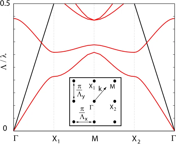
direction) are TM-like. We only consider coupling to TE-like modes (the fiber can couple to either). Furthermore, we assume that the slab is thin enough to ensure that the frequencies of the second order odd modes (which are also TE-like) are above the frequency range of interest, so that only the fundamental TE-like mode needs to be considered. Figure 2.2 shows the approximate bandstructure of the fundamental TE-like modes of the bulk square-lattice PC slab considered in this paper. This bandstructure is calculated using an effective index 2D planewave expansion model that takes into account the finite thickness of the slab but neglects the vector nature of the field, providing a useful guide for analyzing theω−kspace properties of potential PC waveguide modes.
Γ
X
M
X
Γ
0
0.5
Λ
/
λ
1 2
X
X M
Γ
1
2
k
[image:39.612.155.458.106.355.2]Λ
π
xΛ
π
yFigure 2.2: Approximate bandstructure of fundamental even (TE-like) modes for a square lattice PC of air holes with radiusr/Λ = 0.35 in a slab of thicknessd= 0.75Λ and dielectric constant = 11.56. Calculated using an effective index ofneffTE = 2.64, which corresponds to the propagation constant of the fundamental TE mode of the untextured slab. The inset shows the first Brillouin-zone of a rectangular lattice.
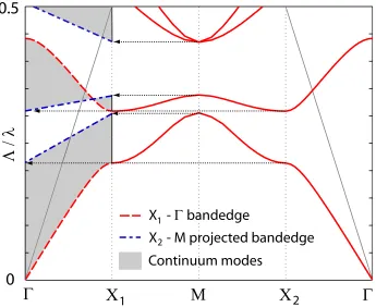
in Fig. 2.3, and by a discrete set of modes whose field is localized to the defect region. In k-space the localized and delocalized modes are characterized by β and a transverse wavenumber distribution. The projection creates continuums of delocalized modes in ω−β
Γ
Γ
Χ
Μ
Χ
Λ / λ
0.5
X -
Γ
bandedge
Continuum modes
0
1 2
[image:40.612.118.463.86.368.2]X - M projected bandedge
2 1Figure 2.3: Projection of the square lattice bandstructure onto the first Brillouin-zone of a line defect with the same periodicity of the lattice and oriented in the X1 → Γ direction.
Bandedges whose modes have dominant wavenumbers in theX1 →Γ direction (i.e. k=kˆz)
are drawn with solid black lines. Bandedges whose modes have dominant wavenumbers in theX2→M direction (i.e. k=kzˆz+π/Λxx) are drawn with dashed black lines.ˆ
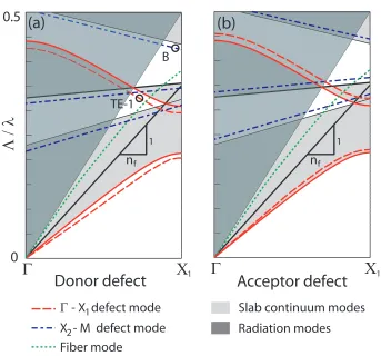
To determine what PC waveguidek-space properties are desirable for efficient coupling, it is necessary to consider the fiber taper mode properties. Guided fiber taper modes are confined to the region inω−β space bounded by the air and fiber (usually silica,nf ≈1.45) light lines, as shown in Fig. 2.4, which immediately limits the PC modes with which the fiber can phase match. A suitable fiber typically has a radius on the order of a PC lattice constant, and the corresponding linearly polarized fundamental fiber mode (HE11±HE1−1)
Γ
Χ
Λ / λ
0
0.5
Γ
Χ
Donor defect
Acceptor defect
Γ- X defect mode
1 1
X - M defect mode Fiber mode
1
2
Slab continuum modes
Radiation modes TE-1
B
(a)
(b)
n 1
f n
1
[image:41.612.154.497.77.397.2]f
Figure 2.4: Approximate projected bandstructure for (a) donor type and (b) acceptor type, compressed square lattice waveguides. Possible defect modes and the fundamental fiber taper mode are indicated by the dashed lines.
direction here).
These ideas are illustrated in Fig. 2.4, which shows a bulk compressed square lattice band structure projected onto the first Brillouin zone of a line defect in the X1 → Γ
mode degenerate inω is detuned sufficiently inβto suppress coupling, due to its large phase mismatch. Although lattice compression is not required to achieve this, it is sometimes advantageous to distort the lattice in order to optimize the window inω−β space, as was done here. Compressing the lattice in the transverse direction effectively raises the energy of the bands at theX2 point and M point in Fig. 2.3, modifying the projection of the full
bandstructure onto the first Brillouin zone of the defect waveguide, as reflected in Fig. 2.4. Once an appropriate lattice and defect waveguide type have been selected, and the ap-proximate location of the desired mode inω−β space determined using these approximate 2D techniques, 3D finite-difference time-domain (FDTD) can be used to numerically cal-culate the field profiles and exact dispersion of the 3D PC waveguide eigenmodes. The numerical results are used in turn in the coupled mode theory to model the coupling to the tapered fiber modes. These design principles are applied in the next section to design a compressed square lattice PC defect waveguide that can couple efficiently to fiber tapers.
2.3
Contradirectional coupling in a square lattice PC
The PC waveguide modes considered in this paper are formed within an optically thin (thicknesstg = 3/4 Λx) semiconductor (n= 3.4) membrane perforated with a square array of air holes. From the approximate band structure for the bulk compressed square lattice waveguide shown in Fig. 2.4, there are several potential defect waveguide modes that are not in a continuum and that can phase match with a fiber taper (whose typical disper-sion is also shown). Of these modes, only waveguide mode A has the desired transverse wavenumber components: It comes off a bandedge projected from theX1→Γ band of the
bulk bandstructure, while the other modes come from M →X2 bandedges. Because mode
TE1 is not in a full frequency bandgap, it is not an obvious candidate in the context of the
existing literature, which focuses on waveguide modes within a full bandgap. However, as we will show, this mode is confined to the defect region, can be coupled selectively with a fiber taper, and can be used to probe high-Q cavity modes (Ch. 3).
Λ / λ
z
β Λ / 2π
z
B
0.4
0.15
0.32
0.5
[image:43.612.196.452.84.408.2]TE-1
TE-1
Figure 2.5: 3D FDTD calculated bandstructure for the waveguide shown in Fig. 2.1(c). The dark shaded regions indicate continuums of unbound modes. The dashed lines are the dispersion of fiber tapers with radiusr = 0.8Λz = 1Λx(upper line) andr= 1.5Λz = 1.875Λx (lower line). The solid black lines are the air (upper line) and fiber (lower line) light lines. The energies and wavenumbers of modes TE1 and B are ˜ωΛz/2π = 0.304 and 0.373 at
βΛz/2π= 0.350 and 0.438 respectively.
of interest (circle “TE1” in Figs. 2.4 - 2.5). Although other donor defect geometries could
have been used, the hole radius grading and the lattice compression used here are important design features of the waveguide for a number of reasons. As discussed in Ch. 3, the field profile of Ref. [76]’s graded cavity mode is very similar to that of waveguide mode TE1
(a)
(b)
(c)
x / Λx 5
-5
z /
Λz
0 2
x / Λx 5
-5
y /
Λz
-2 2
Λx x k / π
-3 3
z /
Λz
0 1
[image:44.612.146.441.86.401.2]-1 1
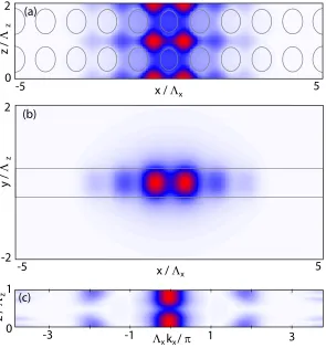
Figure 2.6: Mode TE1 field profiles calculated using FDTD. Dominant magnetic field
com-ponent (a)|By(x, y= 0, z)|; and (b)|By(x, y, z= 0)|; (c) Dominant electric field component transverse Fourier transform |E˜x(kx, y = 0, z)|. Note that the dominant transverse Fourier components are near kx = 0.
donor mode without any stitching of the lattice required. (Choosing ΛPC
x = ΛCavx requires that ΛPCz /ΛCavz = ˜ωCav/ω˜PC.) The two sets of localized states expected from Fig. 2.4 are seen to form, one originating from the X1-point in the 2D reciprocal lattice, and the other
from theM-point. The most localized of each set are the fundamental (transverse) modes, which we label as mode TE1 and modeB in Figs. 2.4 - 2.5. The magnetic field profiles and
the transverse Fourier transforms of these localized modes are shown in Figs. 2.6 - 2.8. The Fourier transforms confirm that the dominant transverse Fourier components of mode TE1
are centered aboutkx = 0, while those of modeBare centered aboutkx=±π/Λx. Both of these modes have negative group velocity, indicating that coupling to them from the fiber will becontradirectional in nature.
0
150
0
1
L /
Λ
|C |
2
j
[image:45.612.170.468.82.497.2]z
| C (0) |-PC 2
| C (L) |+PC 2
| C (L) |+F 2
| C (0) |-F 2
(a)
(b)
ω = ω
0L /
Λ
(ω − ω ) / ω
0 00.025
0.96
0
0
150
0
z
- 0.025
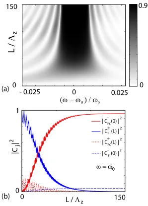
Figure 2.7: (a) Power coupled to PC mode TE1from a tapered fiber with radiusr= 1.15Λx placed with ad= Λx gap above the PC as a function of detuning from phase matching and coupler length. (b) Power coupled atω=ω0 to the forward and backward propagating PC
and fiber modes as a function of coupler length.
fiber taper, and including only those PC and fiber modes that are nearly phase-matched (as well as their backward propagating counterparts) in the coupled mode theory, the mode amplitudes at the coupler outputs were calculated as a function of coupler length and detuning of ω from the phase matching frequency ω0. Figure 2.7(a) shows the resulting
(a)
(b)
(c)
x / Λx 5
-5
z /
Λz
0 2
x / Λx 5
-5
y /
Λz
-2 2
Λ k / x x π
-3 3
z /
Λz
0 1
[image:46.612.145.442.87.400.2]-1 1
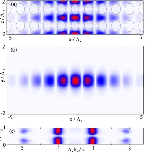
Figure 2.8: Mode B field profiles calculated using FDTD. Dominant magnetic field com-ponent (a) |By(x, y = 0, z)|, (b) |By(x, y, z = 0)|. (c) Dominant electric field component transverse Fourier transform |E˜x(kx, y = 0, z)|. Note that the dominant transverse Fourier components are near kx =±π/Λx.
of coupler length at the phase matching condition. For reference, at an operating wavelength (λ0) of 1.55μm, Λx ≈0.5μm, which corresponds to a taper diameter (2r) of roughly 1μm
and a waveguide-to-waveguide gap (d) of 0.5μm in this case. For ω = ω0 and L = 50Λz the coupled power is greater than 80%, and reaches 95% for L = 80Λz (≈ 40μm). The remaining power is coupled to the backward propagating fiber mode. Note that because the PC mode has negative group velocity, this is contra-directional coupling resulting in monotonically increasing power transfer as a function of coupler length when the transverse coupling is stronger than the detuning in β [78]. The bandwidth is approximately 1.5% of
ω0, and it was verified that within this frequency range coupling to other modes is negligible
model used here this results in stronger coupling to the backward propagating fiber mode and a decreased asymptotic coupling efficiency. In addition, such strong coupling is best modeled using a more complete basis within coupled mode theory or using a fully numerical approach such as FDTD.
To illustrate the importance of a mode’s dominant transverse Fourier components for efficient coupling, Fig. 2.9 shows the power transfer as a function of coupler length and detuning to mode B in Fig. 2.5 from an appropriately phase matched fiber taper placed
d= Λx above the PC1.
Although modeB is even about the mirror plane in the center of the waveguide, because it is constructed from Bloch modes around the M-point it has relatively small amplitude for transverse Fourier components near zero, resulting in a small transverse overlap factor (Kij) with the fiber taper mode. This results in a coupler length ≈200 times longer than that for mode TE1, as well as an extremely narrow bandwidth of≈10−4% ofω0 (a property
further amplified by modeB’s low group velocity). Calculations not shown here that studied acceptor defect modes arising from the valence band edge (M−X2) yield similar results,
despite their very broad field profiles, which would be expected to match well with the fiber. These calculations demonstrate that by selecting a mode composed from the appropri-ate regions in kspace, efficient power transfer between a tapered fiber and the PC can be achieved that is mode selective and that (thanks to its contradirectional character) does not depend critically on the coupling length above some critical minimum. Using a more numer-ically intensive supermode calculation, we now confirm that the simple coupling analysis used above is valid.
2.4
Supermode calculations
In order to verify the coupling picture between the individual waveguide modes presented in the previous section, it is useful to calculate the bandstructure of the hybrid fiber taper-PC waveguide system. Because this system retains the discrete translational symmetry of the PC waveguide, the bandstructure of its modes (the supermodes) can be calculated using FDTD with a combination of Bloch and absorbing boundary conditions in a similar manner
1Besides the very weak coupling between this mode and the fiber taper, higher order odd slab modes may
make coupling in this region ofkspace impractical. Nonetheless, the calculations shown here demonstrate
L /
Λ
(ω
−
ω
0
)
/
ω
00.6
0
0
3000
0
z
- 2.5 x 10
-42.5 x 10
-4Figure 2.9: Power coupled to PC mode B from a tapered fiber with radius r = 1.55Λx placed with ad= Λx gap above the PC as a function of detuning from phase matching and coupler length.
as the bandstructure of the isolated PC waveguide. The resulting bandstructure provides information about the coupling between the modes of the individual waveguides. For weak coupling, it resembles the superposition of the individual waveguide bandstructures (for example Fig. 2.5), but with anti-crossings where the modes intersect and are coupled. The amount of deflection at an anti-crossing is related to the strength of the coupling between the modes, and can be used to back out physical parameters that describe the power transfer.
Figure 2.10(a) shows the bandstructure for a fiber taper of radius r= 1.17Λz = 1.46Λx placed d = Λz = 1.25Λx above the PC waveguide studied in the previous sections. These parameters differ slightly from those used in the previous section, but do not change the results significantly; the larger separation results in a longer coupling length and a smaller bandwidth, while the larger fiber radius lowers the phase matching frequency slightly. The mirror symmetry about the y−z plane of the fiber-PC system is used to filter for modes that are even about this plane, but the fiber breaks the mirror symmetry in the x−z
anti-_
+
Fiber dispersion
Supermode dispersion
_
+
(a)
(c)
(d)
0.27
0.32
0.32
0.40
Λ / λ
z
β Λ / 2π
z
Mode TE-1
x
x
y
-0.5
0
1
0
1
Figure 2.10: (a) FDTD calculated bandstructure of the full fiber taper photonic crystal system. The fiber taper has a radius r= 1.17Λz = 1.46Λx, and is d= Λz = 1.25Λx above the PC waveguide. The TE1-like and fiber-like dispersion is identified, and the symmetric
and antisymmetric superpositions of these modes at the anti-crossing are labeled by the
± signs. (b) The By(x, y,0) component of the symmetric supermode. (c) The By(x, y,0) component of the antisymmetric supermode.
crossing where they intersect indicates that the two modes are coupled. In addition, the fundamental fiber taper mode couples strongly to a series of PC modes at higher frequencies than mode TE1, which was not predicted from the analysis in the previous section. These