A 6.7-GHz Active Gate Driver for GaN FETs to
Combat Overshoot, Ringing, and EMI
Harry C. P. Dymond, Jianjing Wang
, Dawei Liu, Student Member, IEEE, Jeremy J. O. Dalton, Neville McNeill,
Dinesh Pamunuwa, Senior Member, IEEE, Simon J. Hollis, and Bernard H. Stark
Abstract—Active gate driving has been demonstrated to
beneficially shape switching waveforms in Si- and SiC-based power converters. For faster GaN power devices with sub-10-ns switch-ing transients, however, reported variable gate drivswitch-ing has so far been limited to altering a single drive parameter once per switch-ing event, either durswitch-ing or outside of the transient. This paper demonstrates a gate driver with a timing resolution and range of output resistance levels that surpass those of existing gate drivers or arbitrary waveform generators. It is shown to permit active gate driving with a bandwidth that is high enough to shape a GaN switching during the transient. The programmable gate driver has integrated high-speed memory, control logic, and multiple paral-lel output stages. During switching transients, the gate driver can activate a near-arbitrary sequence of pull-up or pull-down out-put resistances between 0.12 and 64Ω. A hybrid of clocked and asynchronous control logic with 150-ps delay elements achieves an effective resistance update rate of 6.7 GHz during switching events. This active gate driver is evaluated in a 1-MHz bridge-leg converter using EPC2015 GaN FETs. The results show that aggressive manip-ulation of the gate-drive resistance at sub-nanosecond resolutions can profile gate waveforms of the GaN FET, thereby beneficially shaping the switch-node voltage waveform in the power circuit. Examples of open-loop active gate driving are demonstrated that maintain the low switching loss of constant-strength gate driving, while reducing overshoot, oscillation, and EMI-generating high-frequency spectral content.
Index Terms—Active gate driver, electromagnetic interference
(EMI), gate signal profiling, GaN FETs, gate overshoot, oscillation, programmable gate resistance.
I. INTRODUCTION
A
CTIVE gate driving dynamically changes the gate resis-tance [1]–[6], gate voltage [7]–[9], or gate current [10]–Manuscript received October 26, 2016; accepted January 31, 2017. Date of publication March 17, 2017; date of current version October 6, 2017. This work was supported by the U.K. Engineering and Physics Sciences Research Council (EPSRC) under Grant EP/K021273/1 and Grant EP/K034804/1. Recommended for publication by Associate Editor B. Chen. (Corresponding author: B. H. Stark.)
H. C. P. Dymond, J. Wang, D. Liu, J. J. O. Dalton, D. Pamunuwa, and B. H. Stark are with the Faculty of Engineering, University of Bristol, Bris-tol, BS8 1UB, U.K. (e-mail: [email protected]; jianjing.wang@ bristol.ac.uk; [email protected]; [email protected]; Dinesh. [email protected]; [email protected]).
N. McNeill is with the Department of Electronic and Electrical Engineer-ing, University of Strathclyde, Strathclyde, G1 1RD, U.K. (e-mail: neville. [email protected]).
S. J. Hollis is with the IBM Research–Almaden Labs, San Jose, CA 95120 United States (e-mail: [email protected]).
Color versions of one or more of the figures in this paper are available online at http://ieeexplore.ieee.org.
Digital Object Identifier 10.1109/TPEL.2017.2669879
[16], with the intention of controlling switching waveforms of power semiconductor devices, as opposed to conventional gate drives that apply a voltage step function to the gate via a fixed resistance. Benefits that have been demonstrated in MOS-gated silicon devices include current balancing in parallel devices [3], voltage balancing in series devices [10], [11], reduction of current and voltage overshoot [4]–[7], [13], suppression of EMI generation without significantly affecting power loss [8], [9], [12]–[15], and optimization of power efficiency under con-stantly changing load conditions [7], [16].
With the move to faster wide-bandgap devices, the need for shaping the switching waveforms increases. Two commonly reported challenges encountered in the application of wide-bandgap devices are voltage overshoots and oscillation [8], [17]– [19]. Conventional methods to address these issues at the source can be divided into two categories:
1) Minimizing parasitic inductances introduced by device packaging and PCB layout: Asdi/dtanddv/dtincrease dramatically in wide-bandgap devices, the amount of par-asitic inductance necessary to generate voltage overshoots or oscillation is greatly reduced [17]. Optimized PCB lay-out techniques cannot eliminate parasitic inductance com-pletely and may even conflict with the requirements for thermal and mechanical design [18].
2) Slowing down the switching speed: With conventional gate drivers, overshoots and oscillation are traded off for increased switching loss, thus undoing some of the benefit of using wide-bandgap devices [8]. In bridge-leg topolo-gies, it also implies an increase in the dead time that further increases power loss [19].
Another reported challenge is that commercially available low-voltage GaN devices exhibit a low margin between the gate-source voltage required to enhance the channel, and the absolute maximum gate-source voltage above which the gate is permanently damaged [20]. Maximum switching speed is thereby limited under conventional gate driving, as there is a minimum gate resistance requirement to avoid overshoot at the gate (see [21], eq. (3.1)]), as illustrated in Fig. 1. By con-trast, active gate driving can achieve the switching speed of a constant gate resistance lower than this minimum requirement, without incurring any gate overshoot (see Fig. 1), as demon-strated later. To fully take advantage of wide-bandgap devices, active gate driving that accommodates more degrees of free-dom for shaping the switching waveforms is therefore highly desirable.
Fig. 1. Minimum allowable gate resistance versus gate loop inductance for a GaN FET with 1-nF input capacitance under conventional (according to [21], eq. (3.1)]) and active gate-driving scenarios.
Fig. 2. Active gate driving for GaN FET in bridge-leg topology.
While some studies in gate voltage profiling for SiC power devices have been reported [1], [5], it remains unclear to what extent GaN devices are controllable via the gate. Reported vari-able gate driving for GaN devices has been limited to local dead-time management [22], single change in driving strength [23], and the use of three gate voltage levels for loss reduction during dead time [24]. Two particular challenges arise: first, the time resolution or bandwidth of the active gate driver must be commensurate with the sub-10-ns-level switching time of GaN devices; second, the low-pass filter composed of driver package, PCB tracks and the input capacitance of the GaN FET makes it harder to deliver a shaped gate signal—high-frequency shaping components may be filtered out, while components around the resonant frequency of the gate-drive loop will be emphasized and give rise to underdamped parasitic oscillation.
In this paper, the first gate driver [25] capable of open-loop active gate driving of GaN devices is demonstrated, and driving strategies are developed. The integrated active gate driver, as illustrated in Fig. 2, can be programmed to vary its output resis-tance every 150 ps, which is shown using a 10-V, 4-A, 1-MHz GaN FET bridge leg.
This paper focusses on three example objectives:
1) turning GaN gates on faster, without incurring gate voltage overshoot;
2) eliminating overshoot in switch-node voltage waveforms; 3) attenuating high-frequency components of switch-node
voltage spectra.
A SPICE modeling technique and a gate driving strategy are proposed, which permit the accurate evaluation of active gate driving for GaN FETs. This modeling takes into account driver, interconnect, layout, and component parasitics, and is validated by experiment. It provides insight into the high-bandwidth cir-cuit currents, which are difficult to measure in compact GaN-based circuits without a significant increase in layout parasitics [21]. The model allows the calculation of switching loss per transient, which is useful in the search for optimized switch-ing waveforms with improved balances of switchswitch-ing loss and power-circuit overshoots, oscillation, and EMI-generating, high-frequency spectral content.
This paper is organized as follows: Section II presents the 150-ps high-speed programmable resistance gate driver for GaN FETs. In Section III, this gate driver is modeled and simu-lated in a GaN-based switching circuit, and gate driving strate-gies for shaping the turn-on and turn-off switching waveforms are provided. Section IV describes the test circuit and mea-surement methods used. Section V shows measured switch-ing waveforms for constant-strength gate drivswitch-ing contrasted against active gate driving that target the aforementioned three objectives. The corresponding spectra and power losses are also provided. Section VI draws conclusions on the potential and lim-itations of the presented method of active gate driving for GaN FETs.
II. HIGH-SPEEDACTIVEGATEDRIVER WITHPROGRAMMABLE
OUTPUTRESISTANCE
A. Overview of the Driver Architecture
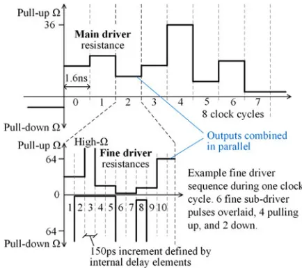
On arrival of a pulsewidth-modulated (PWM) edge, the driver activates a sequence of pull-up and pull-down resistances. This programmable sequence contains the desired output resistances, the polarities (direction of pull, up or down), and the timing values. The driver’s architecture, shown in Fig. 3, comprises three main circuit blocks:
1) An output stage consisting of two parallel drivers: a “main” driver with28output resistance levels and a time resolution adjustable between 1.6 and 2.5 ns, and a “fine” driver with 26 output resistance levels and a time res-olution of 150 ps. The main driver pulls up when the input PWM control signal is logic high and pulls down when PWM is low. In either case, it can alternatively be programmed to be in a high-impedance state if required. Apart from its higher time resolution, the fine driver dif-ferentiates itself from the main driver by being able to either pull up or pull down regardless of the logic stage of the input PWM signal.
2) Memory that holds the gate drive sequences and logic that controls the output stages during transients that are triggered by the PWM signal. This block is controlled by a system clock, and programmed with sequences from external circuitry.
[image:2.594.44.290.242.376.2]Fig. 3. Architecture of the gate driver chip with programmable output resis-tance.
B. Signal Generation to Control the Output Stage
The desired turn-on and turn-off sequences are loaded into a 1024-bit memory by an external controller. The two sequences contain resistances for the main driver and the resistances, tim-ings, and polarities for the fine driver. The data required for the main driver are less, as the fast internal system clock provides its timing, and the PWM edge defines the polarity of pull. Re-sistance sequences are triggered by the PWM signal edges and last for eight clock cycles. An on-chip, voltage-controlled os-cillator (VCO) generates the system clock, variable from 1.6 ns (625 MHz) to 2.5 ns (400 MHz), to permit use for different rise and fall times of the gate transient. The main driver changes resistance on each clock edge. The subclock pulse generator is triggered on each clock edge to produce six pulses of con-trolled delay and duration for the fine driver, during a single clock period. Delay and duration are controllable in increments of 150 ps (equivalent to 6.7 GHz sampling), using selectable delay elements. This allows the sampling frequency to exceed the nominal maximum clock frequency for a given fabrication process. After the eight clock cycles, both drivers retain their final resistance setting until the next PWM transition.
C. Main and Fine Driver
The main driver is a synchronous system, controlled by eight pull-up and eight pull-down signals, which control eight parallel-connected subdrivers, as indicated in Fig. 3. Each subdriver level-shifts its two input signals from 1.8 to 5 V (∼500 ps delay) and buffers them to controlN parallel iden-tical unit driver cells comprising HV PMOS and NMOS FETs (shown in thick line in Fig. 3). The use of identical unit cells ensures consistent timing. The eight subdrivers contain
N = 1, 2,4,8,16,32,64, and 128 identical cells,
respec-TABLE I GATEDRIVERSPECIFICATION
Main Driver Fine Driver Resistance range 0.14–36Ω 1–64Ω
Resistance levels 28(0x01-0xFF) 26(0x01-0x3F)
Time steps 8 11 per main driver step Time resolution 1.6−2.5 ns 150 ps Output polarity Same as PWM Selectable
tively, thus allowing any number of unit cells between 0 and 255 to be selected using 8 bits.
The fine driver is an asynchronous system, controlled by 12 pulse signals with programmable delay and pulse length. These control six parallel-connected subdrivers, which buffer and distribute their two input signals toM parallel identical unit cells (shown in thick line in Fig. 3). These unit cells are cascode connections of fast 1.8-V transistors and slower 5-V in order to attain the required fast resistance change-over. A cascode in the high-side inverts and shifts its input A V to(5−A) V, to enable level-shifting with a delay of only 80 ps. The six subdrivers of the fine driver stage containM = 1,2,4,8,16, and 32 identical unit cells, respectively, thus allowing any number of unit cells between 0 and 63 to be selected using 6 bits.
D. Output Resistance Values and Drive Strength
The selectable drive resistances are 0.14 to 36 Ω for the main driver and 1 to 64Ωfor the fine driver (see Table I). The combined minimum nominal output resistance is 120 mΩ.1
These nominal resistances are defined here as the on-state resistances of the pull-up and pull-down branches of the unit driver cells when 5 V is applied to the respective branches. Under these conditions, the transistors are saturated, and the cell acts as a current source. The resistance against output volt-age of a main driver pull-down NMOS transistor, determined by prelayout simulation using Cadence Spectre, is shown in Fig. 4. The transistor is seen to reduce its on-state resistance from 5 to 2 V, where it is seen to enter the ohmic region. The instantaneous resistance thus varies significantly during active gate driving from the stored programmed nominal resistance. Therefore, simulations in Section III use this characteristic.
In the following sections, for simplicity, resistance sequences are provided using nominal resistances. The maximum resis-tance, where all driver transistors are off, is denoted as “High
Ω.”
E. Degrees of Freedom in the Generation of Drive Resistance Sequences
In each of the eight clock cycles following the PWM edge, the main driver pulls with a constant nominal resistance in the
1The driver is thermally capable of driving continuously into a short circuit, as
Fig. 4. Simulated output characteristics of a single pull-down NMOS transis-tor in the main driver.
Fig. 5. Example of an output resistance sequence.
direction indicated by the PWM signal. In each of these eight clock cycles, the six fine driver substages can be individually delayed (by 0 to 7×150 ps) and then activated for a selectable duration (0, 1, 2, 4, or 6×150 ps), to either pull up or down. This provides many degrees of freedom for the nominal driving sequence, one of which is illustrated in Fig. 5.
The parallel connection of the fine subdrivers forms a se-quence of up to 11 resistance changes per clock cycle. The sequence for each of the eight clock cycles is independently programmable. In the example of Fig. 5, the gate driver is shown transitioning from pull down that holds a power device off to pulling up to a variable degree to shape a turn-on transient.
III. MODELING OFACTIVEGATEDRIVING OFGAN FETS
This section studies whether the programmable driver output can adequately profile the gate-source voltage of a GaN power device despite the effect of the driver package, PCB tracks, and gate impedances of the GaN FETs creating a parasitic low-pass filter between the driver and the GaN FET, and further, whether the achievable profiling is adequate to shape the power-circuit switching waveforms with appreciable benefits.
Fig. 6. Circuit model of the experimental GaN-based bridge-leg circuit used in Section V. Parasitic circuit elements are shown in thick lines.
A GaN FET bridge-leg topology is selected as an evalua-tion platform for waveform shaping, as it incorporates a hard-switched control device and a soft-hard-switched synchronous device in one circuit. Active gate driving can be applied to either or both devices. In this paper, the active gate driver is used to drive the control device only. The gate and source terminals of the synchronous device are shorted, resulting in the equivalent be-havior of a body diode. It is reasonable to hold the gate of the synchronous device off, as both turn-on and turn-off current and voltage commutations happen between the control device and the equivalent body diode of the synchronous device.
A. Circuit Model and Extraction of Parasitics
The SPICE model equivalent to the real bridge-leg circuit in Fig. 2 and used in Section V is shown as in Fig. 6, with a view to investigating hard-switched GaN FET switching behavior under the influence of gate signal profiling. An active gate driver controls the low-side control GaN device. The parasitic elements considered are shown in thick lines.
The active gate driver is modeled as follows: A voltage source
Vdr(t)steps to 5 V for pull-up and back to 0 V for pull-down. There is an on-chip decoupling capacitance whose parasitic in-ductance is negligible; therefore, the parasitic inin-ductance in the gate driver decoupling loop is neglected. Rdr(t, vout)models the varying equivalent output resistance of the active MOS tran-sistors. During pull-down,Rdrequals a third-order polynomial approximation of the voltage-dependent resistanceRdrs of a
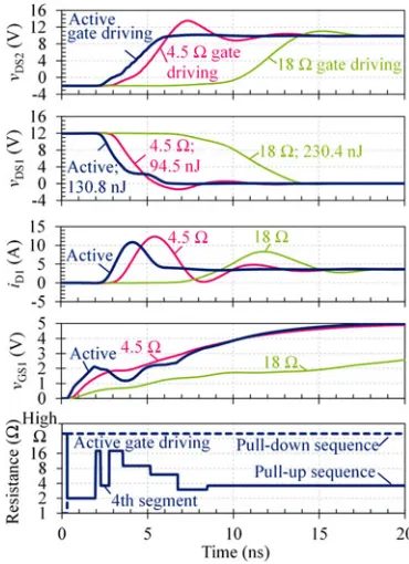
[image:4.594.57.274.237.430.2]Fig. 7. Simulated (solid) and measured (dashed) switching waveforms for
vG S 1,vD S 1, andvD S 2(Fig. 6). Top: turn-on transient with 4.5Ωgate driving.
Bottom: turn-off transient with 4Ωgate driving.
and PMOS transistors in all output stages and is derived from post-layout simulation, the two resulting components being
CDS(NM OS)= 10−10−10−11·VOUT (1)
and
CDS(PM OS) = 10−10−10−11·(5−VOUT). (2)
Based on these approximations, the sum of these capacitances is 150 pF and independent of voltage, which appears to be suffi-ciently accurate for the purpose of using in the model. This ca-pacitance has a significant effect on the gate voltage waveforms prior to reaching the GaN FET’s gate threshold. The parasitic inductancesLdr1 andLdr2of the driver package are extracted using Q3D Extractor and represent the bond-wire inductance. The remaining circuit components and layout-dependent para-sitics of Fig. 6 are derived for the real circuit that is used to verify the simulations in Fig. 7 and to obtain the experimental results of Fig. 16 onward. The inductive load includes interturn capac-itance, derived from the specified self-resonant frequency, and the dc-link capacitors are modeled with equivalent series induc-tance (ESL) and equivalent series resisinduc-tance (ESR) as measured at 1 MHz with 10-V dc bias on a Wayne-Kerr 65120P impedance analyzer. A 0.5-Ωdamping resistance is placed in series with the capacitance closest to the GaN devices. The GaN FETs are modeled using the EPC2015 Spice model available in [26]. The layout-dependent inductances of the power and gate loops are derived by creating a simplified geometric model of the circuit layout and device packages in Q3D Extractor. The model of Fig. 6 also shows nodes representing the Kelvin source connec-tion (SS1) for the gate loop, and the source connecconnec-tion (S1) for the power loop. This separation reduces the effect of the para-sitic source inductance, whose influence on switching losses is significant [19], [21].
The resulting model (see Fig. 6) is simulated in LTspice for load current flowing into the switch node. Fig. 7 shows the sim-ulated switching waveforms compared to measured waveforms,
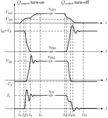
Fig. 8. Representative switching waveforms ofvG S 1,vD S 1,vD S 2, andiD1,
and the delineation of eight control phases.
for constant-strength gate driving using a nominal 4.5Ωfor turn on and 4Ωfor turn off; it is worth recalling that constant nom-inal resistance settings do not provide a constant instantaneous resistance (see Section II-D).
It is apparent that delay times and overshoots are relatively accurate as are the trends and slopes; however, the damping and oscillation frequencies of the model appears to be slightly too low. This could be due to the omission of skin-effect models for the conductors. In the following, this model is used to illus-trate the active gate driving sillus-trategy and find suitable resistance sequences.
B. Gate Driving Strategy
The aim of active gate driving here is to strike a better bal-ance between power-circuit switching-waveform overshoot and the switching loss of the control device. Both the turn-on and turn-off of the synchronous device are soft-switched, generating negligible switching loss during the switching of the control de-vice [21], and thus, the influence of active gate driving on losses in the synchronous devices is not considered in this paper.
[image:5.594.67.260.66.251.2]Turn-on delay time(t1. . . t2): The gate voltage is below the gate threshold voltage,Qcontrolremains off, and the gate driving strength affects primarily the duration of this phase. A strong pull-up is applied to reduce the delay time.
Current rise time (t2. . . t3): The gate voltage controls the commutation of current from Qsync toQcontrol. As the drain current slew rate determines the current overshoot and oscil-lation in the next two phases, the pull-up strength is reduced slightly to slow down the rate of change of current while keep-ing the overlap loss low. Short durations of deviations from this average strength can be used to counteract ringing.
Voltage fall time (t3. . . t4): The pull-up strength is further decreased at the beginning of this phase to reduce the voltage slew rate and the resultant displacement current flowing through
Qcontrol. In order not to greatly increase the overlap loss, the pull-up strength is increased asvDS1approaches zero.
Oscillation time(t4. . . t5): AftervDS1 reaches steady state, the gate driving strength does not affect the oscillation and overshoot iniD1 andvDS2. If necessary, the pull-up strength is briefly reduced to prevent gate overshoot. Afterwards, the pull-up strength is increased to hold the device on.
Likewise, a general gate driving strategy for turn-off transi-tions is proposed.
Turn-off delay time(t6. . . t7): The gate voltage is still above the value whereQcontrol would exit the ohmic region, and the gate driving strength affects mainly the duration of this phase. A strong pull-down strength is applied to reduce the delay time. Voltage rise time(t7. . . t8): The device exits the ohmic re-gion, and the gate voltage controls the voltage slew rate ofvDS1 as long as the channel remains on. A strong pull-down would turn the channel off quickly, leaving the voltage slew rate to be determined by the load current and nonlinear parasitic ca-pacitance at the switch node. Load current is shed intoQsync to discharge its output capacitance, which reduces overlap loss. Therefore, a driving strength is sought that is strong enough to reduce loss but that does not turn off the channel and thereby lose control of the switching. If this does occur, control can be regained by weakening the pull-down or by momentarily pulling up.
Current fall time(t8. . . t9): A weak pull-down is applied at the beginning of this phase to reduce the current slew rate and the resultant voltage overshoot invDS1. In order not to greatly increase the overlap loss, the gate driving strength is increased asvDS1approaches the peak.
Oscillation time(t9. . . t10): AftervGS1falls below the thresh-old voltageVTH, gate driving strength does not affect the oscil-lation or overshoot iniD1andvDS1. If necessary, the pull-down strength is briefly reduced to prevent gate undershoot. After-wards, a strong pull-down is applied to hold the device off.
C. Simulated Application of the Active Gate Driving Strategy
Fig. 9 shows turn-on switching waveforms for two constant-strength and one active gate-driving scenarios. The turn-on switching loss [27]
Esw on =
[image:6.594.336.521.65.320.2](iD1×vDS1)dt+ECo s s (3)
[image:6.594.336.523.379.510.2]Fig. 9. Simulated turn-on waveforms, with constant-strength gate driving (4.5 and 18Ω), and active gate driving (nominal resistance sequence plots at bottom) to eliminate the overshoot.
Fig. 10. SimulatedvD S 2overshoot versus turn-on switching loss with
con-stant and active gate driving.
of each scenario is calculated, and provided in the line labels of the vDS1 graph in Fig. 9. The energy ECo s s that is stored
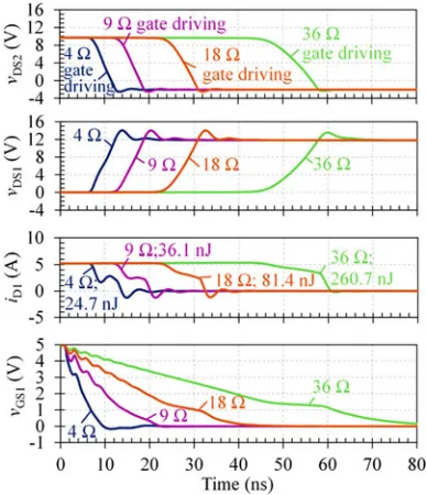
Fig. 11. Simulated turn-off switching waveforms with different constant gate driving strengths.
fourth segment. The final gradual decrease of drive resistance prevents in-circuit oscillation while providing a strong pull-up for the remaining on state. This strategy is seen to eliminate the overshoot, however, with an increase in switching loss by only 38.4%. This is a significantly better trade-off of overshoot against switching loss than 18Ωconstant driving. It is also ob-served that active gate driving has eliminated the oscillation in the displacement current, see the graph ofiD1 in Fig. 9, at the expense of additional spectral content in the shaped gate voltage waveformvGS1.
Fig. 10 plotsvDS2overshoot against turn-on switching loss, for both constant and active gate driving. The constant gate driving strength is swept from 36 to 3Ω, and the active gate driving results are obtained by sweeping the value of the fourth segment of the sequence (starting at 2.3 ns in Fig. 9) from 3.9 to 1.9Ω, where 3.9Ωprovides the waveforms of Fig. 9 and the lowest overshoot. It is apparent that active gate driving is the more efficient way of reducing overshoot.
Fig. 11 shows turn-off switching waveforms for 4, 9, 18, and 36Ωconstant driving, and their respective turn-off switching loss [27]
Esw off =
iD1×vDS1dt−ECo s s (4)
which is provided in the line labels in theiD1graph.
Slowing the turn-off ofQControlusing the 9 or 18Ωsettings has little effect on its voltage overshootvDS1. This is because the channel is turned off before the overshoot begins, as seen by the absence of a gate-voltage Miller plateau. From this point onward, the voltage gradient dvDS1/dt is determined solely by the load current charging the nonlinear GaN FET output capacitances. The weakest gate drive strength (36Ω) reduces the overshoot by 24.3%, as here the channel remains on until the overshoot; however, the switching loss has increased tenfold
Fig. 12. Simulated shaping of turn-off waveforms using active gate driving compared to constant gate driving.
with respect to the 4 Ω switching. It follows that increasing the gate resistance is an unsuitable means of reducing turn-off voltage overshoot in this scenario.
Fig. 12 shows turn-off shaped by active gate driving, against the 4 Ω constant driving waveforms. The active gate driver loses control over turn-off at around 10 ns when the gate sig-nal passes through the threshold voltage, and thevDStransients begin. The driver regains control of the device at around 15 ns after the driver has been in a high-impedance state for 1.8 ns and Miller current has raised the gate voltage. ThevDS1overshoot is reduced by 54.6%, with no apparent slowing of the switching, and a 2.7 times increase in switching loss. This is a marked improvement over the constant drives of Fig. 11. The fact that the delay time does not increase using this method means that short dead times can be maintained, minimizing the time dur-ing which significant reverse conduction loss is incurred in the synchronous GaN FET [19], [21].
[image:7.594.66.260.65.290.2]Fig. 13. Simulated turn-off switching loss versusvD S 1overshoot.
IV. SYSTEMIMPLEMENTATION FORACTIVEGATEDRIVING OFGAN FETS
To test active gate driving in GaN-based converters, a bridge leg of two EPC2015 GaN enhancement-mode FETs is used (see Fig. 2). This circuit replicates the device interaction and hard-switching transitions of a synchronous buck converter.
In contrast to the classic clamped-inductor circuit used for double-pulse testing, the load here containsRo andCo to
fa-cilitate continuous operation where the duty cycle of the PWM signal determines the test current level. This allows the accu-rate measurement of total circuit loss via the dc input and out-put values. In addition, the load is referenced to the high side, which placesQcontrolon the low side; and therefore, measure-ments of gate and device voltages do not have common-mode components. This also permits a ground-referenced gate drive interface. For simplicity, the gate and source terminals of the top GaN FETQsync are shorted, since the driving ofQcontrol actually determines the current and voltage commutations of both devices. Note thatvDS2 is equivalent to the switch-node voltage of a synchronous buck converter.
Near-constant dc-link and gate-drive supply voltages are pro-vided by carefully designed bypass networks incorporating high-frequency damping. The PCB design is optimized follow-ing recommendations in [17] to minimize loop inductance. The circuit board is composed of four layers with 2-ounce copper thickness. The overall board thickness is 0.5 mm. The distance between the top copper layer and the first inner layer is 95µm. The simulated in-circuit power loop inductance is 0.57 nH. Such a low parasitic inductance is required to fully utilize the switch-ing capability of the GaN devices [17]. A higher inductance would worsen the switching waveforms, but would not affect the feasibility of active gate driving.
Fig. 14 shows the power board under test. This test circuit is switched continuously at 1 MHz in order to obtain periodic switching waveforms for frequency-domain analysis. It also al-lows the circuit to reach thermal equilibrium before perform-ing data capture, which is verified usperform-ing a Fluke E30 thermal camera.
[image:8.594.341.521.65.198.2]The test facility is shown in Fig. 15. The PC sends the desired gate drive sequences to a Digilent Zedboard FPGA development board, which programs the gate driver IC. Once programmed, the gate driver is fully autonomous. The programmer uses its
Fig. 14. Detailed view of the test circuit and measurement probes. Not shown is the 2-GHz RT-ZD30 probe connected to the underside of the power board to measure vD S 2.
Fig. 15. Test facility with driver programming, and power and signal mea-surement.
ARM CPU on the Xilinx SoC to communicate with the host PC, to allow the user to change resistance sequences. When a new sequence is sent to the programmer, the PWM signal is interrupted, the gate driver output disabled, new sequences programmed to the driver, the driver re-enabled, and the PWM signal resumed. This control sequence takes place in a few hundred milliseconds.
A pair of 8 GHz Rhode & Schwarz RT-ZZ80 transmission-line probes measure vGS1 and vDS1, while a 2 GHz Rhode & Schwarz RT-ZD30 active differential probe with RT-ZA15 attenuator capturesvDS2. MATLAB, running on the host PC, configures the 4 GHz, 10 GSa/s Rhode & Schwarz RTO1044 oscilloscope to trigger onvDS2 rising edges, and to capture and average 8,192 consecutive waveforms in order to lower the measurement noise floor [8]. The process is repeated forvDS2falling edges. A complete pulse train is reconstructed in MATLAB for analysis.
[image:8.594.341.516.247.439.2]mea-Fig. 16. Measured turn-on switching waveforms showing reduction of gate overshoot by active gate driving.
sured using Keysight U1273A and Fluke 8845A multimeters. The nominal absolute accuracy of the input and output power measurements are each of the order of 100 mW; however, the majority of this is due to temperature dependency of the equipment. Therefore, groups of measurements that are com-pared in Section V are carried out in quick succession at the same temperature. It has been verified that the relative changes in loss as a function of gate driving strategy are repeatable and consistent.
V. EXPERIMENTALRESULTS
A. Experiment 1: Speeding Up Turn On
The aim of this experiment is to demonstrate that active gate driving can suppress gate voltage overshoot and, therefore, allow faster driving than is possible with constant-strength driving. Fig. 16 shows the measured turn-on switching waveforms for three gate-driving scenarios: constant 3.6 and 2Ωdriving and active gate driving, whose nominal resistance sequences are shown in the bottom graph of Fig. 16.
[image:9.594.67.259.66.288.2]3.6Ωdriving provides the fastest turn-on speed of the control GaN FET with no visible overshoot at the gate. 2Ωdriving is seen to not only speed up the switching but also lead to a gate-voltage overshoot to within 0.5 V of the GaN FET’s absolute-maximum gate-source voltage of 6 V. The active driving strat-egy eliminates the gate voltage overshoot while maintaining the speed of 2Ωdriving. The active gate driving strategy of Fig. 16 shows the driver resistance being changed at the frequency of the internal clock using the main drivers only. The maximum time during which changes can be made is eight clock cycles, and in this case, seven changes are made. It is apparent that no subclock changes are made; the fine drivers are inactive. The transition starts with a low resistance, to switch the control device as fast as possible. The resistance is then increased to introduce damping
Fig. 17. MeasuredvD S 1 97%–3% fall time versus gate overshoot for the
[image:9.594.330.523.67.193.2]control GaN FET under constant-strength and active gate-driving scenarios.
Fig. 18. Measured turn-on switching waveforms and power-circuit losses, showing elimination ofvD S 2 overshoot without increased loss, by means of
active gate driving.
into the gate-drive loop. The result is that active gate driving has allowed the speed of 2Ωdriving to be combined with the gate voltage overshoot of 3.6Ωdriving. This is also shown in Fig. 17, where the measured 97%–3% fall time ofvDS1is plotted against voltage overshoot at the gate, for a range of constant driv-ing strengths, and the active gate drivdriv-ing sequence of Fig. 16. Active gate driving achieves a power device switching edge that is faster than constant drive resistances down to 2Ωwhile avoiding the overshoot that the lower resistances incur.
B. Experiment 2: Elimination of Switch-Node Voltage Overshoot
[image:9.594.328.521.235.458.2]Fig. 19. Spectral envelopes, calculated from the measured time-domain data of complete switching cycles, for the three gate-driving scenarios in Fig. 18.
thevDS1graph also include the measured power-circuit loss for the respective operating condition. Constant-strength driving is used for the turn-off edge (not shown), with a value of 4Ωin all three scenarios.
18 Ωconstant gate driving incurs novDS2 overshoot. Any lower resistances show overshoot, with the 4.5Ωdriving pro-ducing a significant overshoot of 4 V, with a reduction in delay by 5 ns, however. The increased speed reduces switching loss, as evidenced by the total circuit loss dropping by 8% from 1.63 to 1.50 W. The net reduction in turn-on switching loss is more than 8% as these power values include other constant losses, such as those incurred at the turn-off edge and the conduction loss ofQsyncwith a shorted gate. It is also worth noting that for 1 MHz switching, approximately 0.12 W of loss is due to the
Cossof the GaN FETs, which is independent of the speed of the transients and which therefore puts a lower bound on switching loss. In this experiment, faster switching is possible but does not noticeably reduce total loss.
In contrast to Experiment 1, the active gate driving sequence now uses one fine driver activation at 2.5 ns, when the resis-tance is seen to change for 300 ps within a 1.6 ns clock period. The turn-on sequence starts at 2Ω, to reach the threshold voltage quickly, which is the reason that the switching delay is reduced by 1 ns relative to constant 4.5Ωdriving. The drive resistance is then increased to slow the switching transition, with the fine drivers briefly adjusting the drive strength in order to optimize the shape of the switching waveform. The drive resistance is then reduced, to ensure the switching transition is completed fast enough to not incur excessive loss but slow enough not to excite any power-circuit resonances. The result is a control-device switching transient as fast as the 4.5Ωconstant-strength case but with novDS2 overshoot, 20% lower delay, and no in-crease in total measured loss.
Frequency transformations of the time-domain data of Fig. 18 are shown in Fig. 19. The high-frequency spectral content of the
vDS2 signal has a special significance in terms of the potential EMI generation. This is because thevDS2 signal is equivalent to the switch-node voltage of a buck converter, which would be connected to an output filter and load. At high frequencies, out-put filters can have reduced effectiveness due to parasitic circuit elements, especially the parasitic capacitance of the choke [28]. The output filter, load, and their interconnection can therefore form a structure which may radiate the high-frequency content that the output filter fails to attenuate. Consequently, a reduc-tion in the high-frequency content of this signal can be beneficial from an EMI perspective.
The inverse relationship between loss and high-frequency spectral content of thevDS2 is apparent for constant-strength driving. Active gate driving alters this relationship by having the same loss as the faster constant-strength driving, but with re-duced spectral content ofvDS2on visual inspection, over most of the spectrum, but in particular in the regions of 400 to 700 MHz and 900 MHz to 1.1 GHz. It is worth considering that these spectra include the contribution of turn off, which reduces the visible net influence of active gate driving on a single edge. It is also worth noting that the simulation results of Fig. 9 indicate that overshoot and subsequent ringing in the device currentiD1 are reduced as well.
This improvement comes at the expense of increased spectral content in thevGS1andvDS1signals. As these signals are inter-nal to the circuit, their associated trace lengths can be kept short relative to the electrical wavelength, and therefore, these signals are unlikely to be radiated efficiently. It is beyond the scope of this paper; however, a valuable area of future research could be to explore the transfer of high-frequency content between internal signals and the switch-node voltage and how this would affect EMC compliance, dependent upon the specific hardware layout and resultant parasitic radiative and conductive structures of particular converters.
Fig. 20. Comparison of waveform shaping with and without use of the fine driver.
Fig. 21. Measured turn-off switching waveforms for a variety of constant gate-driving strengths.
C. Experiment 3: Reduction of the High-Frequency Spectrum of the Switch-Node Voltage
The aim of Experiment 3 is to shape the turn-off edge to reduce high-frequency spectral components of the switch-node waveformvDS2. Fig. 21 shows the measured turn-off switch-ing waveforms for four situations: 4, 9, 18, and 36Ωconstant driving.
4Ωdriving shows a turn-off voltage overshoot onvDS1and a sharp undershoot onvDS2. It is apparent that the gate voltage has dropped below the gate threshold voltage of around 1.5 V, turn-ing the channel off, prior to the rise in device voltage. Therefore, the gate driver is not in control of the device voltage transients. These are instead set by the load current charging the GaN de-vices’ voltage-dependent output capacitances. With increasing gate resistance, the point where loss of control occurs moves to later in the device voltage transients, leading to the
gradi-Fig. 22. Spectral envelopes, calculated from the measured time-domain data of complete switching cycles, for the four gate-driving scenarios in Fig. 21.
ent ofvDS1 being reduced until this point. At 9Ωand below, the gradient and voltage overshoot onvDS1 are independent of gate resistance. With 36Ωdriving, control is maintained until half way into the vDS1 rising edge, and therefore, a reduction in the gradient of the entire voltage rise and a slight reduction in overshoot are obtained. As drive resistance increases from 4 to 36 Ω, a significant increase in switching delay is observed. This is due to an increase in the time taken to discharge the control device’s gate capacitance to the voltage required to exit the ohmic operating region.
[image:11.594.67.262.66.284.2] [image:11.594.66.260.333.504.2]Fig. 23. Measured turn-off switching waveforms under constant-strength and two active gate-driving sequences. The inset in the top graph shows the detail of the end of the switching transition. The bottom trace shows a horizontal zoom of the active gate-driving strength sequence.
The results demonstrate the inextricable inverse relationship, when constant-strength gate driving is used, between circuit loss and high-frequency content of the switch-node voltage. To reduce the EMI generating potential of the circuit, an increase in circuit loss must be accepted.
The 4Ωtransition in the time domainvDS2waveform starts smoothly but has an abrupt end, accompanied by high-frequency ringing, both of which are now targeted by active gate driving as follows: In order for the control device to have influence over the final part of the switching trajectory, it is momentarily turned back on. Fig. 23 shows the measured time-domain waveforms for the turn-off transition under fixed 4Ωdriving (identical to Fig. 21) and for two active gate driving sequences.
[image:12.594.336.522.65.470.2]The sharpness and ringing in thevDS2waveform and the over-shoot invDS1have been visibly reduced. In order to be able to reactivate the control device at the end of the transient, the gate driver’s internal clock period is 2.1 ns. Both active gate-driving sequences contain two fine driver activations which pull up, that is, in opposition to the polarity indicated by the PWM signal. This is seen to reverse the gradient of the control device’s gate-source voltage. Just prior to the 10 ns time point, the main drivers are switched into a high-impedance state in order to maintain the gate-source voltage. The two active gate-driving scenarios differ only in the main driver strengths used from 12 ns onward. The zoomed inset in the top graph shows how these active gate drives significantly reduce both the amplitude of the initial undershoot and the high-frequency oscillations invDS2. The benefits of ac-tive gate driving are clearly observable in the frequency domain,
Fig. 24. Spectral envelopes, calculated from the measured time-domain data of complete switching cycles, for the four gate-driving scenarios in Fig. 21 and the two active gate-driving scenarios in Fig. 23.
as shown in Fig. 24. Also shown here are the power-circuit losses under each gate-drive scenario. As before, the turn-on edges are driven with a constant 12Ωin all three cases.
delay or significant losses. It should be noted that as with the turn-on transition, there is an increase in spectral content on the gate signalvGS1. This method also requires a gate driver with sufficient active duration to target the end of a transient, and the ability to pull in both directions during a transient.
VI. CONCLUSION
Active gate driving of a 40 V, 3.2 mΩGaN FET has been demonstrated for both turn-on and turn-off transitions, using a silicon integrated active gate driver, whose output resistance and direction of pull can be programmed to change up to 88 times and with a 150 ps resolution, during each switching transition. A SPICE modeling method that takes into account circuit layout and component and device parasitics is shown to behave with sufficient high-bandwidth accuracy to analyze the impact of 150 ps resolution active gate driving sequences. An active gate driving strategy is proposed and tested with this model. Exper-imental results show that gate voltage overshoot can be elimi-nated. This allows the switching speed to be increased without running the risk of damaging GaN gates that have a limited voltage margin. Drain-source voltage overshoots at turn-on and turn-off are also eliminated or reduced, without an increase in switching loss. The high-frequency content of the switching waveforms that correspond to the switch-node of a synchronous buck converter has been reduced at both turn on and turn off. This has brought about a smaller increase in switching loss (2.5%) than if the fixed gate resistance is increased. The high-frequency content of the complimentaryvDSand gate signal has increased; however, this is a worthwhile trade-off, as these two signals are internal and less prone to causing radiation. Simula-tions show that active gate driving can also reduce the overshoot and ringing in current waveforms.
Generally, it has been shown that, with respect to constant-strength gate driving, active gate driving for 40 V GaN FETs provides favorable trade-offs between overshoots, oscillations, circuit losses, switching delay, and high-frequency spectral con-tent of both voltage and current. The gate driver can be imple-mented as a separate silicon driver, rather than integrating the driver onto the GaN FET.
Further work will include the application of algorithms such as those in [28] to optimize and adapt drive resistance sequences in real time and the application of the driver to 650 V GaN FETs.
REFERENCES
[1] R. Grezaud, F. Ayel, N. Rouger, and J. Chebier, “An adaptive output impedance gate drive for safer and more efficient control of wide bandgap devices,” in Proc. IEEE Workshop Wide Bandgap Power Devices Appl., Oct. 2013, pp. 68–71.
[2] A. Shorten, W. T. Ng, M. Sasaki, T. Kawashima, and H. Nishio, “A segmented gate driver IC for the reduction of IGBT collector current over-shoot at turn-on,” in Proc. IEEE Int. Symp. Power Semicond. Devices ICs, Mar. 2013, pp. 73–76.
[3] M. Sasaki, H. Nishio, and W. T. Ng, “Dynamic gate resistance control for current balancing in parallel connected IGBTs,” in Proc. IEEE Appl. Power Electron. Conf. Expo., Mar. 2013, pp. 244–249.
[4] R. Hemmer, “Intelligent IGBT drivers with exceptional driving and pro-tection features,” in Proc. Eur. Conf. Power Electron. Appl., Sep. 2009, pp. 1–4.
[5] K. Miyazaki et al., “General-purpose clocked gate driver (CGD) IC with programmable 63-level drivability to reduce Ic overshoot and switching loss of various power transistors,” in Proc. IEEE Appl. Power Electron. Conf. Expo., Mar. 2016, pp. 1640–1645.
[6] J. Gottschlich and R. W. De Doncker, “A programmable gate driver for power semiconductor switching loss characterization,” in Proc. IEEE Power Electron. Drive Syst., Jun. 2015, pp. 456–461.
[7] N. Idir, R. Bausiere, and J. J. Franchaud, “Active gate voltage control of turn-on di/dt and turn-off dv/dt in insulated gate transistors,” IEEE Trans. Power Electron., vol. 21, no. 4, pp. 849–855, Jul. 2006.
[8] N. F. Oswald, P. Anthony, N. McNeill, and B. H. Stark, “An experimental investigation of the tradeoff between switching losses and EMI generation with hard-switched all-Si, Si-SiC, and all-SiC device combinations,” IEEE Trans. Power Electron., vol. 29, no. 5, pp. 2393–2407, May 2014. [9] N. F. Oswald, B. H. Stark, D. Holliday, C. Hargis, and B. Drury,
“Anal-ysis of shaped pulse transitions in power electronic switching waveforms for reduced EMI generation,” IEEE Trans. Ind. Appl., vol. 47, no. 5, pp. 2154–2165, Sep.–Oct. 2011.
[10] P. R. Palmer and A. N. Githiari, “The series connection of IGBTs with active voltage sharing,” IEEE Trans. Power Electron., vol. 12, no. 4, pp. 637–644, Jul. 1997.
[11] I. Baraia, J. A. Barrena, G. Abad, J. Segade, and U. Iraola, “An ex-perimentally verified active gate control method for the series connec-tion of IGBT/diodes,” IEEE Trans. Power Electron., vol. 27, no. 2, pp. 1025–1038, Feb. 2012.
[12] Y. Lobsiger and J. W. Kolar, “Closed-loop di/dt and dv/dt IGBT gate driver,” IEEE Trans. Power Electron., vol. 30, no. 6, pp. 3402–3417, Jun. 2015.
[13] B. Wittig and F. W. Fuchs, “Analysis and comparison of turn-off active gate control methods for low-voltage power MOSFETs with high current ratings,” IEEE Trans. Power Electron., vol. 27, no. 3, pp. 1632–1640, Mar. 2012.
[14] X. Yang, Y. Yuan, and P. R. Palmer, “Shaping high-power IGBT switching transitions by active voltage control for reduced EMI generation,” IEEE Trans. Ind. Appl., vol. 51, no. 2, pp. 1669–1677, Mar./Apr. 2015. [15] M. Blank, T. Gl¨uck, A. Kugi, and H. Kreuter, “Digital slew rate and
S-shape control for smart power switches to reduce EMI generation,” IEEE Trans. Power Electron., vol. 30, no. 9, pp. 5170–5180, Sep. 2015. [16] Z. Zhang, J. Fu, Y. F. Liu, and P. C. Sen, “Adaptive current source
drivers for efficiency optimization of high-frequency synchronous buck converters,” IEEE Trans. Power Electron., vol. 27, no. 5, pp. 2462–2470, May 2012.
[17] D. Reusch and J. Strydom, “Understanding the effect of PCB lay-out on circuit performance in a high-frequency gallium-nitride-based point of load converter,” IEEE Trans. Power Electron., vol. 29, no. 4, pp. 2008–2015, Apr. 2014.
[18] J. Popovic, J. A. Ferreira, J. D. van Wyk, and F. Pansier, “System integra-tion of GaN converters—Paradigm shift,” in Proc. Int. Conf. Integr. Power Syst., Feb. 2014, pp. 1–8.
[19] E. A. Jones, F. Wang, and B. Ozpineci, “Application-based review of GaN HFETs,” in Proc. IEEE Workshop Wide Bandgap Power Devices Appl., Oct. 2014, pp. 24–29.
[20] Efficient Power Conversion, EPC2015—Enhancement Mode Power Tran-sistor. (2013).[Online]. Available: epc-co.com
[21] A. Lidow, J. Strydom, M. de Rooij, and D. Reusch, GaN Transistors for Efficient Power Conversion, 2nd ed. New York, NY, USA: Wiley, 2015.
[22] R. Grezaud, F. Ayel, N. Rouger, and J. Crebier, “A gate driver with integrated dead-time controller,” IEEE Trans. Power Electron., vol. 31, no. 12, pp. 8409–8421, Dec. 2016.
[23] M. K. Song, L. Chen, J. Sankman, S. Terry, and D. Ma, “16.7 A 20 V 8.4 W 20 MHz four-phase GaN DC-DC converter with fully on-chip dual-SR bootstrapped GaN FET driver achieving 4ns constant propagation delay and 1ns switching rise time,” in Proc. IEEE Int. Solid-State Circuits Conf., Feb. 2015, pp. 302–303.
[24] X. Ren, D. Reusch, S. Ji, and Z. Zhang, “Three-level driving method for GaN power transistor in synchronous buck converter,” in Proc. IEEE Energy Convers. Congr. Expo., Sep. 2012, pp. 2949–2953.
[25] H. C. P. Dymond et al., “Reduction of oscillations in a GaN bridge leg using active gate driving with sub-ns resolution, arbitrary gate-resistance patterns,” in Proc. IEEE Energy Convers. Congr. Expo., Sep. 2016, pp. 1–6. [26] http://epc-co.com/epc/DesignSupport/DeviceModels, Jul. 2015. [27] Y. Xiong, S. Sun, H. Jia, P. Shea, and Z. J. Shen, “New physical insights
[28] S. Wang, F. C. Lee, and J. D. van Wyk, “Design of inductor winding capacitance cancellation for EMI suppression,” IEEE Trans. Power Electron., vol. 21, no. 6, pp. 1825–1832, Nov. 2006.
[29] D. J. Rogers and B. Murmann, “Digital active gate drives using sequential optimization,” in Proc. IEEE Appl. Power Electron. Conf. Expo., Mar. 2016, pp. 1650–1656.
Harry C. P. Dymond received the M.Eng. and Ph.D. degrees in electrical and electronic engineering from the University of Bristol, in 2003 and 2010, respec-tively. His thesis involved the development of a high-performance, high-bandwidth AC active load for the evaluation of audio amplifier efficiency.
His research interests include audio, analog, and switch-mode power electronics. Currently, he is a Senior Researcher with the University of Bristol’s Electrical Energy Management group, developing next-generation gate driving techniques for GaN power devices.
Jianjing Wang received her B.Eng. degree in control science and engineering from Huazhong University of Science and Technology, Wuhan, China, in 2009, and the Ph.D. degree in power electronics from City University of Hong Kong, Hong Kong, in 2014.
She is currently a Research Associate with Elec-trical Energy Management group at the University of Bristol. Her research interests include active gate driving for WBG devices, and high-fidelity measure-ment of fast switching transients.
Dawei Liu (S’14) received the B.S. and M.S. degree in Microelectronics from Harbin Institute of Technol-ogy, Harbin, China, in 2005 and 2007, respectively. He is currently with the Electrical Energy Manage-ment group at the University of Bristol, as a Ph.D. student and Research Associate.
His research interests are analogue and power IC design, high-speed gate driver design.
Jeremy J. O. Dalton received his M.Eng. degree in electrical and electronic engineering from University of Bristol, in 2014. He is now working toward the Ph.D. degree with the Electrical Energy Management group at the same university.
His research interests include active gate driving and wide bandgap devices and applications.
Neville McNeill received the M.Phil. and Ph.D. de-grees in power electronics from Napier University, Edinburgh, Scotland, in 2003 and 2008, respectively. His career has included periods working for elec-tric vehicle and renewable energy companies. From 2004 to 2016 he was at the University of Bristol, Bris-tol, England, where he was latterly Senior Lecturer in Power Electronics. He is now Senior Research Fellow in Power Electronics at the University of Strathclyde, Glasgow, Scotland. His main research interests are in high-efficiency multi-kilowatt power electronic con-version for aerospace, renewable energy and electric vehicle applications.
Dr McNeill is a Member of the Institution of Engineering and Technology, a Chartered Engineer with the Engineering Council of the U.K., and a Fellow of the Higher Education Academy.
Dinesh Pamunuwa (M’04–SM’09) received the B.Sc. degree in electrical and electronic engineer-ing from the University of Peradeniya, Sri Lanka, in 1997, and the Ph.D. degree in Electronic System De-sign from the Royal Institute of Technology (KTH), Stockholm, Sweden, in 2003. During his Ph.D. he interned at the Berkeley Research Labs of Cadence Design Systems in Berkeley, CA, working on timing and signal integrity analysis in integrated circuits.
He was appointed to a Lectureship at Lancaster University in May 2004 and made a Senior Lecturer in 2010. He joined the Electrical and Electronic Engineering Department of the Merchant Venturers School of Engineering, University of Bristol as a Reader in Microelectronics in 2011. He works on technologies for the realisation of next generation computing platforms.
Simon J. Hollis received the M.A. and Ph.D. de-grees in computer science from Cambridge Univer-sity, U.K., in 2004 and 2007, respectively.
From 2007 to 2015 he was a Lecturer in computer science at the University of Bristol, UK, research-ing energy efficient computresearch-ing, many-core systems, processor energy measurement, and high-speed pro-grammable drivers. He is now with IBM.
Bernard H. Stark received the M.S. degree in elec-trical engineering from the Swiss Federal Institute of Technology (ETH), Zurich, in 1995, and the Ph.D. degree in engineering from Cambridge University, U.K., in 2000.
![Fig. 1.Minimum allowable gate resistance versus gate loop inductance for aGaN FET with 1-nF input capacitance under conventional (according to [21],eq](https://thumb-us.123doks.com/thumbv2/123dok_us/1376288.90892/2.594.44.290.242.376/minimum-allowable-resistance-versus-inductance-capacitance-conventional-according.webp)