Volume 2012, Article ID 764084,7pages doi:10.1155/2012/764084
Research Article
Detailed Theoretical Model for Adjustable Gain-Clamped
Semiconductor Optical Amplifier
Lin Liu,
1Craig Michie,
1Anthony E. Kelly,
2and Ivan Andonovic
11Department of Electronic and Electrical Engineering, University of Strathclyde, Glasgow G1 1XW, UK 2Department of Electronics and Electrical Engineering, University of Glasgow, Glasgow G12 8LT, UK Correspondence should be addressed to Ivan Andonovic,[email protected]
Received 1 October 2011; Revised 7 February 2012; Accepted 11 February 2012
Academic Editor: Luciano Mescia
Copyright © 2012 Lin Liu et al. This is an open access article distributed under the Creative Commons Attribution License, which permits unrestricted use, distribution, and reproduction in any medium, provided the original work is properly cited.
The adjustable gain-clamped semiconductor optical amplifier (AGC-SOA) uses two SOAs in a ring-cavity topology: one to amplify the signal and the other to control the gain. The device was designed to maximize the output saturated power while adjusting gain to regulate power differences between packets without loss of linearity. This type of subsystem can be used for power equalisation and linear amplification in packet-based dynamic systems such as passive optical networks (PONs). A detailed theoretical model is presented in this paper to simulate the operation of the AGC-SOA, which gives a better understanding of the underlying gain clamping mechanics. Simulations and comparisons with steady-state and dynamic gain modulation experimental performance are given which validate the model.
1. Introduction
Semiconductor optical amplifiers (SOAs) have attracted considerable attention during the last two decades, for use in evolving optical communication networks. SOAs can be used as not only optical amplifiers, but also signal processing devices such as wavelength converters [1], optical switches [2], and electro-optical mixers [3]. In terms of optical ampli-fication, the key issue of operating SOAs is the management of the input optical signal power, which must be maintained within the linear regime of operation; otherwise the device would be driven into saturation causing unwanted inter-symbol interference (ISI) or patterning. In order to solve this implementation problem, many different types of gain-clamped semiconductor optical amplifiers (GC-SOAs) have been proposed [4,5]. Recently, an adjustable gain-clamped semiconductor optical amplifier (AGC-SOA) designed to maximize the output saturated power at a clamped gain which can be adjusted was reported [6].
2. AGC-SOA
The AGC-SOA is a semiconductor optical amplifier topology which has the unique capability to provide variable gain and
maintain linear operation through gain clamping over a wide (40 dB) dynamic range, without compromising the saturable output power of the device [6]. A key advantage of this approach is that there are no mechanical tuning elements, and hence the gain can be adjusted via direct electrical con-trol at ns timescales. While the operation of this device has been presented previously for the static gain case [6], and its behaviour under dynamic gain modulation conditions [7], the underlying mechanics is not well understood. Here, a theoretical model for an AGC-SOA has been established, based on the wideband steady-state numerical model of a SOA [8]. The travelling amplified spontaneous emission (ASE) power and spectrum within a ring cavity, steady-state, and dynamic gain modulation have been studied. Simula-tions are in broad agreement with experiment results.
Figure 1illustrates conceptually the design of the
SOA1 200 mA
WDM WDM
SOA2 variable current
P C C P
[image:2.600.315.544.72.259.2]R R
Figure 1: Counterpropagating ring laser adjustable gain-clamped
SOA (AGC-SOA) implementation.
12 10 8 6 4 2 0
−2
0 5 10 15 20 25
Gain (dB)
Psat
[image:2.600.54.287.72.136.2](dBm)
Figure 2:Psat(dBm) variation as a function of SOA gain (dB).
by controlling the drive to SOA2, the gain imparted by SOA1 can be adjusted. SOA1 is continually operated at full current, and therefore, the AGC-SOA allows signals to be amplified by SOA1 at a clamped gain which is varied by SOA2. This maximises the saturation output power thereby maintaining an extended linear regime [6].
The key advantage that the AGC-SOA offers over other optical amplifiers is that it enables the gain to be adjusted directly through the drive current to the clamping SOA without the dramatic loss ofPsat. Hence, linear operation is maintained over a wider range of input signals. In standard SOAs, it is possible to adjust the gain by altering the drive current however, as is demonstrated in the experimental measurement shown inFigure 2, and this leads to a dramatic loss inPsat.
At high gains, where the SOA is highly inverted, thePsat
value is at its highest. However, in this region, adjusting the small signal gain through bias current has a dramatic effect on thePsatvalue. In the example depicted inFigure 2, at high gains thePsatchanges with gain at a rate of∼3 dBm/dB i.e., for every dB that the gain is reduced, thePsatvalue drops by 3 dBm. As the drive current is further reduced, the drop inPsatwith gain is weaker at∼0.4 dBm/dB. However, by the time that this point has been reached, thePsatvalue is already significantly compromised (5 dBm compared to the high gain value of 10 dBm). The AGC-SOA enables gain modu-lation to be achieved without this dramatic loss ofPsatvalue.
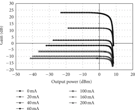
Figure 3depicts the gain of AGC-SOA as a function of
output power for a set of different clamping currents ranging from 0 mA to 200 mA. ThePsatvalues are constant over the range of clamping currents despite significant gain reduction (>20 dB), demonstrated inFigure 4.
−50 −40 −30 −20 −10 0 10 20
30 25 20
10 15
5 0
−5
−10
−15
−20
Output power (dBm)
Gain (dB)
0 mA 20 mA 40 mA 60 mA
100 mA 160 mA 200 mA
Figure 3: AGC-SOA gain as a function of output power at different clamping currents. Legend: bias current of SOA2.
16 14 12 10 8 6 4 2 0
−15 −10 −5 0 5 10 15 20 25
Gain (dB)
Psat
[image:2.600.59.283.190.327.2](dBm)
Figure 4:Psat(dBm) variation as a function of AGC-SOA gain (dB).
Additional steady-state experimental results such as gain, Noise Figure (NF), andPsatvalue were demonstrated in [6]. The dynamic gain modulation performance of AGC-SOA was further studied in [7]. In a dynamic packet equalisation scenario, the AGC-SOA is able to adjust and stabilise its gain in less than 2 ns, within the period of the guard band of the passive optical network (PON) transmission at 1.25 Gbit/s on the upstream direction, 32 bit periodsis equates to 26 ns. Similarly for 10-Gigabit-capable, PON system, the guard time is 64 bits at 2.5 Gbit/s on the upstream direction [9], this equates to 26 ns [9].
3. Model of AGC-SOA
[image:2.600.315.542.307.481.2]Table 1: Device parameters used in AGC-SOA simulation.
Symbol Parameters SOA1 SOA2
Lc Central active region length 400μm 840μm
Lt Tapered active region length 200μm 160μm
d Active region thickness 0.4μm 0.1μm
W Active region width 0.4μm 1.1μm
y Molar fraction of arsenide 0.892 0.816
Γ Confinement factor 0.15 0.15
R1 Input facet reflectivity 5×10⁻⁵ 1×10⁻⁵
R2 Output facet reflectivity 5×10⁻⁵ 1×10⁻⁵
ηin Input coupling loss 3 dB 2 dB
ηout Output coupling loss 3 dB 2 dB
K0 Carrier-independent absorption loss coefficient 6200 m−1 3000 m−1
K1 Carrier-dependent absorption loss coefficient 7.5×10⁻²¹m2 6.83×10⁻²¹m2
n1 Active region refractive index 3.22 3.56
C1
Recombination coefficients
3.7×10⁸s−1
C2 5.6×10⁻¹⁶m3/s
C3 3×10−41m6/s
αcoupler WDM coupler pass band insertion loss 0.5 dB
j n
1
Output ASE
Output ASE
SOA2
j n
1 ASE
from SOA2
SOA2 forward
ASE testpoint SOA1
Input
signals signals
SOA1 backward
ASE testpoint
[image:3.600.58.285.339.536.2]Output
Figure 5: Schematic of the simulation model for an AGC-SOA.
spontaneous emission (ASE) power still remains largely un-known. In this study, the wideband steady-state SOA model [8] is adapted to form a ring cavity; the evolution of travelling ASE power and spectrum within the ring cavity, important for gain clamping, is then characterised. The gain, Noise Figure (NF), and maximum output power at gain saturation (Psat) of an AGC-SOA under different clamping currents are
also studied. Based on this model, the timescale for adjusting and stabilising the gain, crucial for dynamic packet equalisa-tion, is evaluated.
As shown inFigure 5, ASE circulating within the AGC-SOA travels in clockwise and counterclockwise directions, however, the isolator in the ring cavity ensures that ASE trav-elling in the clockwise direction is not amplified. Thus, the
counterclockwise ASE generated by both SOAs accounts for gain clamping. In this model, the two SOAs are simulated as independent modules using different sets of material param-eters summarised in Table 1. (Typical bulk SOA parame-ters from [8,14,15]). Both SOAs generate ASE in the forward and backward directions in the active regions. In each SOA, the ASE profile extends over 1300 nm ∼1650 nm and is partitioned into discrete frequency bands.
In order to simulate the wideband ASE profile for a single SOA, the material gain coefficient of the SOA active region in an InGaAsP direct bandgap bulk material is given by [8,16]
gm(ν,n)= c
2
4√2π3/2n2
1τν2
2memhh
(me+mhh)
3/2
×
∞
0
ν−Eg h
1/2
×fc(ν)−fν(ν)
×
2T0
1 + (ν−ν)2
(2πT0)2
dν
= c2
4√2π3/2n2
1τν2
2memhh
(me+mhh)
3/2
×
ν−Eg
h
1/2
×fc(ν)−fν(ν)
,
(1)
wherecis the velocity of light in vacuum,νis the optical fre-quency,n1is the active region refractive index,τis the
radia-tive carrier recombination lifetime,is the normalized Plan-ck constant,meis the effective mass of an electron in conduc-tion band (CB),mhhis the effective mass of a heavy hole in
valence band (VB),Egis the band gap energy of the material, T0is the mean lifetime for the coherent interaction of
[image:3.600.319.548.473.616.2]The gain coefficient can be divided into two parts: stimu-lated emission rateReand stimulated absorption rateRa,
gm(ν,n)=Re(ν,n)−Ra(ν,n), (2)
where
Re(ν,n)= c
2
4√2π3/2n2
1τν2
2memhh
(me+mhh)
3/2
×
ν−Eg
h
1/2
×fc(ν)
1−fν(ν),
Ra(ν,n)= c
2
4√2π3/2n2
1τν2
2memhh
(me+mhh)
3/2
×
ν−Eg
h
1/2
×fv(ν)
1−fc(ν)
.
(3)
The propagation of optical field in the SOA can be des-cribed as
dA+
j
dz = −iβ+
1 2
Γgm(ν,n)−α
A+
j,
dA−j
dz = iβ−
1 2
Γgm(ν,n)−α
A−j,
(4)
whereA+
j andA−j are the forward and backward travelling waves of the jth active region section, respectively,βis the propagation constant,Γis the confinement factor, andαis the internal loss coefficient.
The propagation of the spontaneous emission field is pre-sented as
dS+
k dz =
Γgm(νk,n)−α
S+
k+Rsp(νk,n),
dS−k dz =−
Γgm(νk,n)−α
S−k −Rsp(νk,n).
(5)
S+
k andS−k are the forward and backward amplified spontane-ously emitted photon densities per unit frequency spacing centred at frequency νk. Rsp(νk,n) is the ASE noise
cou-pled into S+
k or S−k, and it is expressed as Rsp(νk,n) =
ΓRe(νk,n)Δν,Δνis frequency spacing. The carrier rate equation is presented by
dn(Z)
dt =
I
qV −R(n(z))− n
j=1
Γgm(ν,n)
Across
A+
j +A−j
−
m
k=1
2Γgm(νk,n)
Across
S+
k+S−k
.
(6)
The recombination rate termR(n(z)) is given by
R(n)=C1n+C2n2+C3n3, (7)
whereC1,C2, and C3 are the nonradiative recombination,
bimolecular radiative recombination, and auger recombina-tion coefficients, respectively.
The numerical model for the whole system ofFigure 5is achieved using iterative circulations. In the first iteration, the ASE in both directions of SOA2 is calculated assuming no
0 5 10 15 20 25 30 35 12 10 8 6 4 Loops ASE po w er (dBm)
[image:4.600.315.543.70.229.2]SOA1 backward ASE power SOA2 forward ASE power
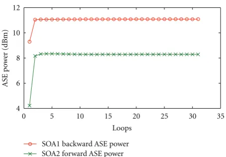
Figure 6: Counterclockwise ASE power afterNloops. Cross: SOA2 output ASE power. Circle: SOA1 output ASE power.
ASE power is coupled in. Then the ASE generated by SOA2 travels in both clockwise and counterclockwise order towards SOA1. Under this boundary condition, the ASE originated from SOA2 together with the one generated by SOA1 is amp-lified by SOA1 as it travels through; however, only the back-ward ASE inside the SOA1 is input to SOA2. For any succes-sive iterations, the ASE from SOA1 couples into SOA2 be-fore SOA2 generates ASE. When ASE travels inside the ring cavity, the facet reflectivity and coupling loss of both SOAs, the insertion loss for the isolator, and WDM couples are taken into account. The round trip time is∼1.67 ns namely, the fibre length is about 0.5 m. Therefore, fibre loss and dispersion are neglected. The iterative procedure is terminat-ed when the maximum difference of the ASE powers at each discrete frequency band between successive iterations is less than the desired tolerance. The numerical model is impleme-nted using Matlab.
4. Simulation Results and Discussions
The characteristics of AGC-SOA were studied from the initial state when no input signal is introduced. The ASE power after every counterclockwise ASE round trip is recorded.
InFigure 6, the counterclockwise output ASE powers from
SOA2 and SOA1 are displayed after each loop transit. The ASE power increases rapidly within the first 3 loops and then stabilises. Since the cavity round trip time is
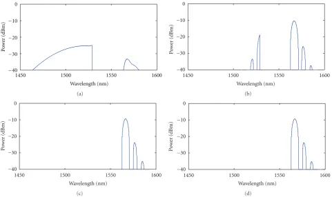
∼1.7 ns, stabilising the travelling ASE power in the loop takes between 1.7 and 5.1 ns (several round trips). The ASE spec-trum within the clamping mode was examined after every circulation. Figure 7 shows the SOA2 output ASE spectr-um at different loop transits. In the first loop, the output ASE power from SOA2 is relatively low, and the whole spectrum is divided into two parts falling outside the C-band due to presence of the WDM coupler in the ring cavity.
[image:4.600.71.289.102.256.2]Initially, the ASE power within the S-band is greater than that within the L-band. However, as the lasing mode becomes established, the output ASE power develops as predicted in
Figure 6. With the ASE power within the S-band decreasing
1450 1500 1550 1600 0
−10
−20
−30
−40
Wavelength (nm)
P
o
w
er (dBm)
(a)
1450 1500 1550 1600
−40 −30 −20 −10 0
Wavelength (nm)
P
o
w
er (dBm)
(b)
1450 1500 1550 1600
−40 −30 −20 −10 0
Wavelength (nm)
P
o
w
er (dBm)
(c)
1450 1500 1550 1600
−40 −30 −20 −10 0
Wavelength (nm)
P
o
w
er (dBm)
[image:5.600.60.542.72.358.2](d)
Figure 7: Modeled SOA2 ASE spectrum (counterclockwise). (a) Loop number=1; (b) loop number=10; (c) loop number=20; (d) loop number=100.
0 5 10 15 20 25
−2 −1.5 −1 0
Loops after signal added
Si
gn
al gain (dB)
−0.5
Figure 8: CW light (1550 nm, −20 dBm) gain as a function of circulating ASE loops after AGC-SOA stabilisation.
As ASE circulations progress, ASE emission in the S-band is further restrained becoming negligible, and ASE within the L-band accounts for gain clamping. This results from the fact that the lasing threshold is lower at longer wavelengths hence once lasing action is established, the shorter wavelength energy states are depleted. The results agree well with experi-mental observation.
Having established the steady-state conditions of model operation, an input optical signal was introduced after the ASE inside the AGC-SOA cavity stabilizes. The gain of 1550 nm CW light as a function of travelling ASE loop num-bers is depicted in Figure 8. An optical signal power of −20 dBm was injected into SOA1. The drive current of SOA1
was set at 200 mA, and SOA2 at 65 mA. The simulation demonstrates that the signal gain settles within the first ASE loop transit and then remains unchanged; thus, after AGC-SOA stabilizes from the initial state (shown in the evolution depicted inFigure 7), it takes<2 ns (within one loop time) for the gain to settle.
The variation of the gain with clamping SOA drive cur-rent was modelled over a range of clamping curcur-rents to cor-roborate that the model faithfully reproduced the experim-ental behaviour of the AGC-SOA. The model outputs
(Figure 9) indicate broadly that the model is predicting the
trends. There is no significant loss ofPsatwith gain
reduc-tion, however, the exact values of gain andPsatdiffer slightly
from experimental measurements. This difference most like-ly derives from small differences between the physical para-meters used in the model and the real device.
The DC parametric operation of the AGC-SOA can be estimated using the above model. CW light (1550 nm) was introduced into AGC-SOA once the steady-state operation was established. The input signal power was then increased steadily from−35 dBm to 20 dBm, and the normal perfor-mance metrics of gain, maximum output power at gain satu-ration (Psat), and noise figure (NF) were recorded for a given
[image:5.600.55.288.413.543.2]−40 −30 −20 −10 0 10 20 −20
−10 0 10 20 30
0 mA 20 mA 40 mA
60 mA 80 mA
Output power (dBm)
Fiber
-t
[image:6.600.56.287.70.238.2]o-fiber gain (dB)
Figure 9: AGC-SOA gain as a function of output power at different clamping currents (modeling result).
50 150 200
−20 0 20 40
Gain (dB) and NF (dB)
0
Gain
100
0 5 10 15 20
Noise figure
Output satur
ation po
w
er (dBm)
Control current (mA)
−5
[image:6.600.315.542.73.203.2]Psat
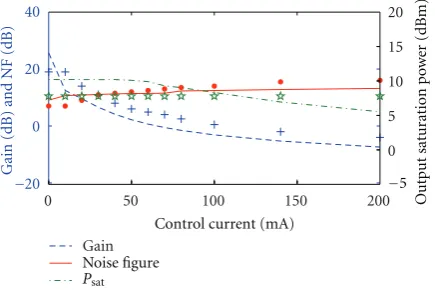
Figure 10: Experimental [6] and theoretical steady-state AGC-SOA performance comparisons. Red line: simulation results of NF. Red dot: experimental results of NF. Blue line: simulation results of gain. Blue cross: experimental results of gain. Green line: simulation results ofPsat. Green star: experimental results ofPsat.
0 mA. Experimentally this value was observed to be nearer 10 mA before there was sufficient gain within the clamping SOA to overcome loop losses and allow the lasing mode to stabilize. This difference is mainly due to the overestimation of ASE noise within the model [8]. Strong clamping is ob-served when the control SOA is operated at high gain levels; here, the AGC-SOA is driven into attenuation. As the gain is clamped, the NF increases, but in the main, thePsatvalue
re-mains relatively constant when the clamping current is
<100 mA.
The theoretical model could also be used to better under-stand the dynamic behaviour of the AGC-SOA. In order to do this, the model was run under the following conditions. Firstly, stable operation of the AGC-SOA was ensured by running the simulation with only ASE for the first 30 loop iterations and at an SOA2 (clamping SOA) bias of 20 mA. At this point, a 0 dBm input signal was introduced, and it can be seen that the gain of the AGC-SOA is around 10 dB. The clamping SOA bias current was then increased every 10
0 20 40 60 80 100 120 140
−10 −5 0 5 10
Loops
[image:6.600.63.281.293.438.2]Gain (dB)
Figure 11: Dynamic gain variation as a function of clamping
current.
loops, from 20 mA to 200 mA, in steps of 20 mA and the gain change observed (Figure 11). It is clear from these simula-tions that the gain is indeed adjusted and stabilized within 1 or 2 loops of the model iteration. This implies therefore that the gain can be adjusted within nanosecond timescales which agree with experimental results [7].
5. Conclusion
A detailed wideband model for adjustable gain-clamped semiconductor optical amplifier (AGC-SOA) has been estab-lished, which can be used to analyse steady-state and dyna-mic gain modulation performance of the device. The simula-tions agree with the experimental results, showing the advan-tage of AGC-SOA not only lies in extended linear amplifica-tion regime and adjustable device gains, but also the ability of adjusting and stabilising its gain within nanosecond time-scales. This feature could enable the device to work as power equalizer and linear amplifier in packet-based dynamic sys-tems such as passive optical networks (PONs).
Acknowledgments
Strathclyde University gratefully acknowledges funds receiv-ed from the British Council under the Prime Ministers Initia-tive II, Research Cooperation. This work was also supported in part by the Glasgow Research Partnership in Engineering (GRPe).
References
[1] L. Banchi, M. Presi, A. D’Errico, G. Contestabile, and E. Cia-ramella, “All-optical wavelength 10 and 40 Gbit/s RZ-to-NRZ format and wavelength conversion using semiconductor opti-cal amplifiers,” Journal of Lightwave Technology, vol. 28, no. 1, pp. 32–38, 2010.
[3] C. Boh´emond, A. Sharaiha, T. Rampone, and H. Khaleghi, “Electro-optical radiofrequency mixer based on semiconduc-tor optical amplifier,” Electronics Letters, vol. 47, no. 5, pp. 331– 333, 2011.
[4] P. Doussiere, F. Pommereau, J. Y. Emery et al., “1550 nm polar-ization independent DBR gain clamped SOA with high dyna-mic input power range,” in Proceedings of the 22nd European
Conference on Optical Communication (ECOC ’96), vol. 3, pp.
169–172, September 1996.
[5] D. A. Francis, S. P. DiJaili, and J. D. Walker, “A single-chip lin-ear optical amplifier,” in Proceedings of the Optical Fiber
Com-munication Conference, pp. PD13/1–PD13/3, Anaheim, Calif,
USA, March 2001.
[6] C. Michie, A. E. Kelly, I. Armstrong, I. Andonovic, and C. To-mbling, “An adjustable gain-clamped semiconductor optical amplifier (AGC-SOA),” Journal of Lightwave Technology, vol. 25, no. 6, pp. 1466–1473, 2007.
[7] L. Liu, C. Michie, A. E. Kelly, and I. Andonovic, “Packet equal-isation in PONs using adjustable gain-clamped semiconduct-or optical amplifiers (AGC-SOA),” in Proceedings of the
Inter-national Conference on Transparent Optical Networks (ICTON ’11), pp. 1–4, Stockholm, Sweden, June 2011.
[8] M. J. Connelly, “Wideband semiconductor optical amplifier steady-state numerical model,” IEEE Journal of Quantum
Ele-ctronics, vol. 37, no. 3, pp. 439–447, 2001.
[9] ITU-T Recommendation G.987.2, “10-Gigabit-capable pas-sive optical networks (XG-PON): physical media dependent (PMD) layer specification,” January 2010.
[10] X. H. Jia, “Theoretical investigation of gain-clamped semi-conductor optical amplifiers using the amplified spontaneous emission compensating effect,” Journal of the Optical Society of
America B, vol. 23, no. 12, pp. 2503–2510, 2006.
[11] A. Matsumoto, K. Nishimura, K. Utaka, and M. Usami, “Oper-ational design on high-speed semiconductor optical ampli-fier with assist light for application to wavelength converters using cross-phase modulation,” IEEE Journal of Quantum
Elec-tronics, vol. 42, no. 3, Article ID 01597418, pp. 313–323, 2006.
[12] C. Y. Jin, Y. Z. Huang, L. J. Yu, and S. L. Deng, “Detailed model and investigation of gain saturation and carrier spatial hole burning for a semiconductor optical amplifier with gain cla-mping by a vertical laser field,” IEEE Journal of Quantum
Elec-tronics, vol. 40, no. 5, pp. 513–518, 2004.
[13] S. Verspurten, G. Morthier, and R. Baets, “Experimental and numerical small-signal analysis of two types of gain-clamped semiconductor optical amplifiers,” IEEE Journal of Quantum
Electronics, vol. 42, no. 3, Article ID 01597417, pp. 302–312,
2006.
[14] S. L. Chuang, Physics of Optoelectronic Devices, Wiley-Inter-science, New York, NY, USA, 1995.
[15] M. J. Connelly, “Wide-band steady-state numerical model and parameter extraction of a tensile-strained bulk semiconductor optical amplifier,” IEEE Journal of Quantum Electronics, vol. 43, no. 1, pp. 47–56, 2007.
Submit your manuscripts at
http://www.hindawi.com
Hindawi Publishing Corporation
http://www.hindawi.com Volume 2014
High Energy PhysicsAdvances in
World Journal
Hindawi Publishing Corporation
http://www.hindawi.com Volume 2014
Hindawi Publishing Corporation
http://www.hindawi.com Volume 2014
Fluids
Journal ofAtomic and Molecular Physics Journal of
Hindawi Publishing Corporation
http://www.hindawi.com Volume 2014 Hindawi Publishing Corporation
http://www.hindawi.com Volume 2014
Condensed Matter Physics
Optics
International Journal of
Hindawi Publishing Corporation
http://www.hindawi.com Volume 2014
Hindawi Publishing Corporation
http://www.hindawi.com Volume 2014
Astronomy
Advances inInternational Journal of Hindawi Publishing Corporation
http://www.hindawi.com Volume 2014
Superconductivity
Hindawi Publishing Corporation
http://www.hindawi.com Volume 2014 Statistical Mechanics
International Journal of
Hindawi Publishing Corporation
http://www.hindawi.com Volume 2014
Gravity
Hindawi Publishing Corporation
http://www.hindawi.com Volume 2014
Astrophysics
Journal ofHindawi Publishing Corporation
http://www.hindawi.com Volume 2014 Physics
Research International
Hindawi Publishing Corporation
http://www.hindawi.com Volume 2014
Solid State PhysicsJournal of
Computational Methods in Physics
Journal of
Hindawi Publishing Corporation
http://www.hindawi.com Volume 2014
Hindawi Publishing Corporation
http://www.hindawi.com Volume 2014
Soft Matter
Hindawi Publishing Corporation http://www.hindawi.com
Aerodynamics
Journal ofVolume 2014
Hindawi Publishing Corporation
http://www.hindawi.com Volume 2014
Photonics
Hindawi Publishing Corporation
http://www.hindawi.com Volume 2014 Journal of
Biophysics
Hindawi Publishing Corporation
http://www.hindawi.com Volume 2014