UNIVERSTI TEKNIKAL MALAYSIA MELAKA
:;' AKULTI KEJURliTERAAN ELEKTRONIK DAN KEJURUTERAAN KOMPliTER BORANG PENGESAHAN STATUS LAPORAN
PROJEK SARJANA MUDA II
FPGA IMPLEMENTATION OF AES ALGORITHM
Tajuk Projek
Sesi Pengajian
.MEJ MOHD Y AZI BIN ABDUL RAHMAN Say a
(HURUF BESAR)
mengaku membenarkan Laporan Projek Satjana Muda ini disimpan di Perpustakaan dengan syarat -syarat kegunaan seperti berikut:
1. Laporan adalah hakmilik Universiti Tek:nikal Malaysia Melaka.
2. Perpustakaan dlbenarkan membuat sa1inan untuk tujuan pengajian sahaja.
3. Perpuscikaan dlbenarkan membuat sa1inan laporan ini sebagai bahan pertukaran antara institusi
pengajian tinggi.
4. Sila tandakan ( ..J ) :
D
SULIT*D
TERHAD**EZI
TIDAK TERHAD(TANDA AN PENUUS)
9.'2
June 2016Tarik.h: ... ..
*(Mengandungi maklwnat yang berdaijah keselamatan atau kepentingan Malaysia seperti yang termaktub di dalam
AKTARAHSlARASMI 1972)
**(Mengandungi maklumat terhad yang telah ditentukan oleh organisasi!badan di mana penyelidikan dijalankan)
Disahkan oleh:
~
(COP DAN T AND AT ANGAN PENYEUA)
PROf. OR. ZULKALNAIN BIN MOHO YUSSOF Profesor .
Fakulti Kejuruteraan Elektronik Oa_n KeJuruteraan Kolmputel
Uni•ersiti Teknikal Malays.a Meiaka (UTeM
Hang Tuah Jaya
.
J:1,.
June 1B\~ ourian Tunggal. Me\ak>Tarik.h: ... .
vi
ACKNOWLEDGEMENT
Alhamdulillah, firstly I am grateful to almighty Allah S.W.T because at last I manage to complete and finish my Final Year Project and my Thesis successfully. It is impossible to finish this report without the help and guidance from whoever involve either directly or indirectly.
Despite of that, I would like take this opportunity to express my profoundest gratitude and deepest regards to all those who gave me the possibility to successfully complete this PSM. I am deeply indebted to my Project Supervisor Prof Dr Zulkalnain bin Mohd Yussof and I wish to express million thanks for his guidance, constant encouragement and monitoring throughout the development of the project.
vii
ABSTRACT
viii
ABSTRAK
tesis ini membentangkan pelaksanaan FPGA algoritma Advanced Encryption Standard (AES). AES adalah teknik penyulitan untuk maksud melindungi data sensitif
dan berharga daripada dipintas oleh pihak yang tidak diingini. AES digunakan secara meluas dalam aplikasi kerajaan, tentera dan perbankan. Algoritma AES boleh dilaksanakan menggunakan High Level Bahasa seperti C / C ++ berjalan pada pemproses tujuan am atau perkakasan. Walau bagaimanapun, bagi masa sebenar aplikasi berkelajuan tinggi, algoritma AES perlu dilaksanakan dalam perkakasan kerana keperluan pengiraan yang tinggi. Dalam projek ini, AES dipetakan kepada seni bina digital selari untuk mendapatkan pelaksanaan kelajuan tertinggi. AES seni bina digital dimodelkan menggunakan Verilog coding, simulasi dan fungsinya disahkan menggunakan ISim Xilinx ISE Design Suite. Keputusan simulasi membuktikan fungsi adalah betul untuk Verilog AES Model. Reka bentuk AES telah disintesis dan dilaksanakan pada FPGA. System Generator Hardware Co-simulasi digunakan untuk
ix
TABLE OF CONTENTS
CHAPTER CONTENT PAGE
TITLE OF PROJECT i
BORANG PENGESAHAN STATUS LAPORAN ii
STUDENT’S DECLARATION iii
SUPERVISOR’S DECLARATION iv
DEDICATION v
ACKNOWLEDGEMENT vi
ABSTRACT vii
ABSTRAK viii
TABLE OF CONTENTS ix
LIST OF TABLES xii
LIST OF FIGURES xiii
LIST OF ABBREVIATION xvi
LIST OF APPENDIXES xvii
I INTRODUCTION 1
x
11 LITERATURE REVIEW 5
2.1 Chapter Overview 5 2.2 Previous Project 6 2.3 Encryption 8 2.3.1 Symmetric Cryptography 9 2.3.2 Advance Encryption Standard 9 2.4 Field Programmable Gate Array 10 2.5 Verilog 12 2.6 ISE Xilinx Design Suite 14.7 13
III METHODOLOGY 15
xi
IV RESULT AND DISCUSSION 43
4.1 Chapter Overview 43 4.2 Result on Encryption Process 43 4.2.1 Simulation Result Substitute Bytes 44 4.2.2 Simulation Result of Shift Row 44 4.2.3 Simulation Result of Mix Columns 46 4.2.4 Simulation Result of Key Expansion 48 4.2.5 Data Encryption Using 256 Bit Key 52 4.3 Decryption Process 53 4.3.1 Simulation Result Inverse Substitute Bytes 53 4.3.2 Simulation Result Inverse Shift Row 54 4.3.3 Simulation Result Inverse Mix Columns 55 4.3.4 Key Expansion Operation 56 4.3.5 Simulation Result of Key Expansion 56 4.3.6 Data Decryption Using 256 Bit Key 58 4.4 System Generator Hardware Co-simulation 59 4.5 Result on FPGA Implementation 60 4.6 Discussion 62
V CONCLUSION AND RECOMMENDATION 63
5.1 Conclusion 64 5.2 Future Recommendation 64
xii
LIST OF TABLES
NO TITLE PAGE
xiii
LIST OF FIGURES
NO TITLE PAGE
xiv
3.18 Block Diagram of Encryption Operation 34 3.19 Inverse Substitute Operation of State Array 35 3.20 Diagram for Inverse Substitute Byte of 128 bit input 36 3.21 Diagram of Inverse Shift Row Operation 36 3.22 Matrix State Diagram of Inverse Shift Row Operation 37 3.23 Matrix State Diagram of Inverse Mix Columns Operation 37 3.24 Block Diagram of Decryption Operation 39 3.25 Verilog Code 40 3.26 Isim ISE Xilinx Suite Simulation Result 41 3.27 System Generator Hardware Co-simulation 41 3.28 Embedded FPGA 42 3.29 Evaluating Process Using Spartan 6 LX150T 42 4.1 Simulation Result for Byte Substitution of 32 bit input 44 4.2 Simulation Result for Substitute Byte of 128 bit input 44 4.3 Simulation Result for Shift Row Transformation 45 4.4 Simulation Result for Mix Column Operation of 32 Bit input 46 4.5 Simulation Result for Mix Column Operation of 128 Bit input 47 4.6 Simulation Result for Rotation Word of Key Expansion 48 4.7 Simulation Result for Key Expansion of 256 bits 48 4.8 Reference from Federal Information Processing Standards
Publication 197 49 4.9 Simulation Result for Overall Key Expansion 50 4.10 Simulation Result for Data Encryption 52 4.11 Reference from Federal Information Processing Standards
Publication 197 for Plaintext Input Data and Private Key 53 4.12 Reference from Federal Information Processing Standards
Publication 197 for Ciphertext Output Data 53 4.13 Simulation Result for Inverse Substitute Byte of 128 bit input 53 4.14 Simulation Result for Inverse Shift Row of 128 bit input 54 4.15 Simulation Result for Inverse Mix Columns of 128 bits 55 4.16 Reference from Federal Information Processing Standards
xv
4.19 Reference from Federal Information Processing Standards
Publication 197 for Cipher Input Data and Private Key 59 4.20 Reference from Federal Information Processing Standards
xvi
LIST OF ABBREVIATION
AES - Advance Encryption Standard FPGA - Field Programmable Gate Array I/O - Input/Output
VHDL - Verilog Hardware Description Language DES - Data Encryption Standard
FIPS - Federal Information Process Standard DSP - Digital Signal Processing
GF - Galois Field S-Box - Substitute Box RotWord - Rotation Word RCon - Round Constant Func 1 - Function 1 Sel - Select En - Enable Clk - Clock MUX - Multiplexer
RTL - Register-transfer level CLB - Configurable Logic Block LUT - Lookup Table
xvii
LIST OF APPENDIXES
NO TITLE PAGE
1
CHAPTER I
INTRODUCTION
1.1 Project Background
Secure communication is very important aspect in communication where it give a security assurance during the activity of voice conversation, video conference, image and data transfer. It needs a significant and reliable process to ensure when transferring the data it is in secure condition for sender to receiver in communication system and vice versa. To make sure data is secured and protected from being intercepted by others parties, the system need to have an encryption and decryption of data. Encryption is the translation of data to a secret code. Apart from it is uses in military and government to facilitate secret communication. Encryption also used in protecting many kinds of civilian system such as Internet e-commerce, Mobile networks, automatic teller machine transactions (ATM) and many more applications. Encrypted data can only be deciphered when it has the password or private key. Private keys is collection of data bits only known by authorized people who only involve in that particular communication system. It is very important to manage the key from being known by unauthorized person. The key needs to be private or secret to maintain confidentiality.
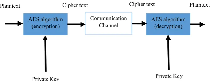
2 Institute of Standard and Technology (NIST) [1]. AES is a Symmetric algorithms based on the kind of Keys used. Symmetric algorithm is an algorithm that using same private key in both sender and receiver part. The process of encryption and decryption need to have same key in both side of sender and receiver. The function of Private Key is important to encrypt and decrypt process of data or information. AES is an algorithm that applies encryption method to convert plaintext to ciphertext and decryption is method to convert the ciphertext to plaintext.
Figure 1.1: Typical Data Encryption and Decryption
The main purpose of this project is an implementation FPGA of AES algorithm. The encryption and decryption using AES algorithm with 128 bits data input and 256 bits of Private Key. The 128 bits of data input is a standard data input and the private key is the options either using 128 bits key, 192 bits key or 256 bits key. This algorithm consists of 4 stages in encryption such as Substitute Bytes stage, Shift Row stage, Mix Columns stage and Add Round Key stage. The decryption stage consists of reverse process of encryption such as Inverse Substitute Bytes stage, Inverse Mix Columns stage and Add Round Key. Another essential component in AES is key expansion. Detailed explanation of the key expansion scheme is given in Chapter 3.
AES algorithm (encryption)
Communication
Channel AES algorithm (decryption)
Plaintext Plaintext
Private Key Private Key
3
1.2 Project Objective
The objectives of this project is to model the digital architecture of AES algorithm using Verilog coding, simulate and verify the functionality using ISim Xilinx ISE Design Suite. Then, to Synthesize and implement to verify the design in hardware on FPGA. Next, to verify the design using System Generator Hardware Co-simulation in FPGA.
1.3 Problem Statement
In communication system, the major concern is about how to protecting secret data from being intercepted by other parties. In order to protect the data from being intercepted it require a strong and reliable process. Cryptography is the system or method that widely used to protect data. The cryptanalysis around the world, always concern on this matter and they always try to develop the significant process to overcome this problem. The encryption and decryption process are involve with the mathematical analysis and it provide the reliable approach. In military, government sector and public communication, the requirement of protecting the data process is very important in order to assure the higher confidential during the communication process. In military communication, they always dealing with the higher degree of secret data such as order, location information and secret code. This is need an uncompromised system that allow the data transfer without any worry and prejudice. Enemy is always try to access or obtain the valuable secret data of military activities and others information.
4 and multi choices of 128 bits key, 192 bits key or 256 bits key that provide better performance in encrypt and decrypt data.
1.4 Scope of Project
To achieve the design and progression of the project, the scope of the project have been identified and divided into two main parts, which are simulation in software and verify in hardware.
Developing the digital architecture of AES algorithm with 128 bits data input and 256 bits of Private Key, is the initial stage of this project. In this stage, well understanding and strong knowledge of algorithm is required in order to understand all the stages in encryption and decryption process. In software simulation process, the ISim Xilinx ISE Design Suite and System Generator Hardware Co-simulation software been used to model and synthesize using Verilog coding and simulate it. Verilog coding is uses to modelling the stages in AES algorithm such as Substitute Bytes, Shift Row, Mix Columns, Add Round Key, Key Expansion, Inverse Substitute Bytes, Inverse Shift Row and Inverse Mix Columns. The compiling Verilog coding of all stages algorithm is to produce the overall process in encryption and decryption data.
5
CHAPTER II
LITERATURE REVIEW
2.1 Chapter Overview
This chapter has gathered the summarized information of the relevant studies to develop the FPGA implementation of AES algorithm. This chapter also carried out the whole project to gain knowledge and skills needed to complete this project. The main sources for this project are the previous project and thesis that related to the project. The other sources of literature review are journals, articles and information from books and internet. Those sources help to identify problem as well as giving an ideas for analysis and decision making in this project. So, this chapter discuss about the project and thesis related to the project.
6
2.2 Previous Project
According to Shivaraj.G.Nanden and Sharanagouda (2014), Cryptography technology has changed the world today by being able to carry data found in physical world to the electronic world with confidence. Hundreds of thousands of people interact electronically every day, whether it is through email, e-commerce, e-bank or cellular phone. As the network speed upgrades to the gigabits per second, the software-based implementations of cryptographic algorithm would not meet it is needed. The hardware-based implementations can greatly improve throughout and reduce the key generation time. The process of cryptographic algorithms and the key generation packaged in chip, which is not easily be read or changed by external attacker. The hardware-based implementations can offer the higher physical security. In recent year, hardware based implementation use the Field Programmable Gate Array (FPGA) and Application Specific Integrated Circuit (ASIC) lacks of flexibility and high development costs and long development cycle. FPGA with hardware of security and high speed and software of flexibility and easy maintenance [1]. Based on this journal, it shows the important of this AES algorithm to be implemented in communication system in nowadays. This journal also suggesting with the future work that concentrate on implementation of AES algorithm using 192 bits key or 256 bits key size. With this reasons, this project was implemented using the AES algorithm with 256 bit key size with reason for efficiency that using with large key size for security of data.
7 implement the algorithm is 128 bits also it means it execute the 10 rounds. The algorithm commences with Add round key stages followed with 9 rounds of four stages and also the last round consists only 3 stages. The 4 stages is Substitute Bytes, Shift Rows, Mix Columns and Add Round Key. The final round execute the Substitute Bytes, Shift Rows and Add Round Key only. Throughout the decryption process, it execute a similar number of rounds however in inverse direction process. The 4 stages involve is Inverse Substitute Bytes, Inverse Shift Rows, Inverse Mix Column and Inverse Add Round Key. Substitute Bytes perform byte substitution that is based on a multiplicative inverse of the finite field. Shift rows shifts components from a particular row by an offset comparable to the row number. Mix Column steps transforms each column using invertible linear transformation. Add Round Key steps takes 4 x 4 blocks from an expanded key, and XORs it with all the ‘state’. The Verilog HDL code is use to implement the algorithm and simulated it using the ISE Xilinx software. The design was develop and tested on a Xilinx Spartan III XC3S400 FPGA [2]. This article also described the important of securing the data in communication system. It also shows the AES algorithm is the approved and reliable algorithm that can execute the encryption and decryption process in software-based and hardware-based.