City, University of London Institutional Repository
Citation
:
Xu, Q., Chen, T., Hu, Y. & Gong, P. (2014). Write Pattern Format Algorithm for
Reliable NAND-Based SSDs. IEEE Transactions on Circuits and Systems II: Express Briefs,
61(7), pp. 516-520. doi: 10.1109/TCSII.2014.2327332
This is the accepted version of the paper.
This version of the publication may differ from the final published
version.
Permanent repository link:
http://openaccess.city.ac.uk/8194/
Link to published version
:
http://dx.doi.org/10.1109/TCSII.2014.2327332
Copyright and reuse:
City Research Online aims to make research
outputs of City, University of London available to a wider audience.
Copyright and Moral Rights remain with the author(s) and/or copyright
holders. URLs from City Research Online may be freely distributed and
linked to.
City Research Online:
http://openaccess.city.ac.uk/
[email protected]
Write Pattern Format Algorithm (WPFA) for
Reliable NAND-based SSDs
Quan Xu, Thomas M. Chen,
Senior Member, IEEE,
Yu-peng Hu, and Pu Gong
Abstract—This paper presents and evaluates a pre-coding algo-rithm to reduce power consumption and improve data retention in NAND-based solid-state drives (SSD). Compared to the state-of-the-art asymmetric coding and stripe elimination algorithm (SPEA), the proposed write pattern format algorithm (WPFA) achieves better data retention while consuming less power. The hardware for WPFA is simpler and requires less circuitry. The performance of WPFA is evaluated by both computer simulations and FPGA implementation.
Index Terms—Solid-state drive, reliability, NAND flash mem-ory, power consumption.
I. INTRODUCTION
N
AND flash memory is the most popular storage tech-nology for solid-state drives due to its non-volatility, lightweight package, and low-power consumption. Basically, each NAND flash cell consists of a floating gate transistor whose threshold voltage can be programmed by injecting certain amounts of charge into the floating gate [?]. For multi-level cell (MLC) NAND flash, one memory cell generally stores more than one bit belonging to different pages that are sequentially programmed at different times. Considering two-bit/cell MLC as an example, the cell threshold voltages, denoted by Vth, are divided into four adjacent levels (L0 $11, L1 $ 01, L2 $ 00, L3 $ 10) after the sequential programming.
Loss or gain of charge occurring on the floating gate over time will lead to bit flipping and consequently retention failures. Experimental measurements have suggested that bit flipping errors are not random but asymmetric; specifically, only “0 !1” errors occur in the lower pages and “1 ! 0” errors are dominant in the upper pages [?]. Hence, in order to reduce the retention error rate, it is useful to distribute more 1’s to lower pages while more 0’s to upper pages, in other words, program most of the cells to states “11” and “01” and fewer cells to “10.
Besides retention reliability, another practical problem is the increasing power required for scaling to larger bit-line capacitances. In SSDs, more power is being consumed to charge or discharge the parasitic capacitance of the bit-lines (BLs). The average current consumed during programming is given by
Ipre=Cbl
V Tpre
nbl (1)
Quan Xu, Thomas M Chen, and Pu Gong are with the School of Engineer-ing and Mathematical Sciences, City University London, EC1V 0HB, U.K. (e-mail:{Quan.Xu.1, Tom.Chen.1, Pu.Gong.1}@city.ac.uk)
Yu-peng Hu is with the Hu Nan University, Changsha 410082, P.R. China. (e-mail: [email protected])
1 0 1 0 d2n-1d2n
d2n-2
d2n-3
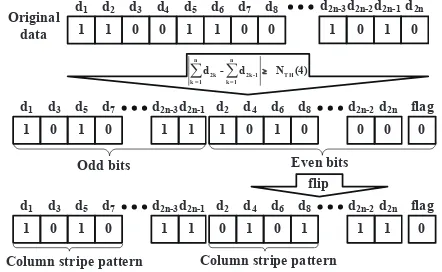
1 1 1 0 1 0 0 0 0 1 0 1 0
d1 d3 d5 d7 d2n-3d2n-1 d2 d4 d6 d8 d2n-2d2n flag
flip Odd bits Even bits Original
data
Column stripe pattern Column stripe pattern
¦n ¦n 2k 2k-1 TH k=1 k=1
d - d N (4)
1 1 1 0 1 0
d1 d3 d5 d7 d2n-3d2n-1
0 1 0 1 1 1 0 d2 d4 d6 d8 d2n-2d2n flag
0
[image:2.612.327.548.180.316.2]1 1 0 1 1 0 0 d1 d2 d3 d4 d5 d6 d7 d8
Fig. 1: Example of SPEA
wherenbl the number of bit-lines charged in parallel; V is
the change of bit-line voltage applied in a program operation; Cbl is the capacitance; and Tpre is pre-charging time [? ].
If the programming data contains too many column stripe patterns (CSPs), these bit-line capacitances will be charged and discharged frequently during the programming, increasing the current flow (and SSD power consumption) and possibly leading to malfunctions [? ].
Several approaches have been proposed to address the problems of data retention and power [? ? ? ? ? ]. Among these, asymmetric coding and the stripe pattern elimination algorithm (SPEA) proposed by Tanakamaru et al. [? ] have been shown to perform well by processing data patterns. In the first step, asymmetric coding calculates the number of 1’s in the input data which is then used to determine whether the bits within the unit are flipped or not. As a result, the distribution of 1’s becomes asymmetric, and the number of cells at highVth
decreases. Secondly, SPEA calculates the difference between the numbers of 1’s in even and odd columns of the original data. If the difference is higher than a threshold value, bits will be rearranged to eliminate the CSPs, which relieves the power problem.
Even though asymmetric coding and SPEA improve SSD performance considerably, their implementation is fairly com-plex especially when the code length of SPEA increases. Meanwhile, additional CSPs are introduced during the SPEA processing which could cause power problems as well. Con-sider the example shown in Fig. 1 where the threshold value, denoted asNT H, is set to 4, and SPEA is applied since the
calculated difference is higher than NT H. After rearranging,
2
0 0 1 0
Do not flip Half flip
0 1 1
1st
stage 2nd
stage
NAND cell area overhead
Data unit 1
Flag e.g. data unit length: 4
0 1 0 1 0 1 1 1
Half flip All flip Do not flip Do not flip
0 0 1 0 1 1 1 1 1 1 0 1
1 1 0 1 1 1 1 1 1 1 0 1
[image:3.612.363.512.56.169.2]Data unit 2 Data unit 3
Fig. 2: Proposed WPFA
to the problems above with low complexity implementation. We first present a write pattern format algorithm (WPFA) that carries out asymmetric processing and stripe elimination simultaneously, which allows data patterns to be modified only once before being fed to an error correction coding (ECC) module. Here it should be noted that the advantages of the solution comes at the cost of a small loss of perfor-mance compared to asymmetric coding. WPFA will achieve an improvement over the original SPEA approach by avoiding the extra CSPs introduced in SPEA and reducing power consumption. The hardware circuitry for WPFA is shown to use fewer gates and registers, and improve system complexity and latency. Simulation and implementation results show a considerable reduction of both NAND cell overhead and FPGA resource utilization. The trade-offs between complexity and performance are analyzed quantitatively.
II. WRITEPATTERNFORMATALGORITHM
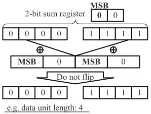
Fig. 2 illustrates an example of the proposed WPFA with lower page input data. The presented solution has two primary stages. The first stage modifies the program data to eliminate the column stripe patterns; the secon stage increases the number of 1’s. Note that the length of data processing unit has been restricted to 2n with n = 2,3,4,5, . . . (although
n = 2 is not practical). Initially, all bits of the data unit are added together and the result is stored in ann-bit sum register. For example, in Fig. 2, the length of data unit is 4 bits and the width of the sum register is 2 bits. The flag in the figure is the most significant bit (MSB) of the sum register which indicates whether the majority of bits in the data unit are 0 or 1. WPFA eliminates CSPs in the following way. If the flag equals 0, the data unit is passed unmodified to the next processing stage, such as “data unit 1” in Fig. 2. If the flag equals 1, a column stripe sequence is added to the input data, and the modulo-2 result is taken as “first stage data”, in other words, half of the input data will be flipped. In the example shown in Fig. 2, both “data unit 2” and “data unit 3” are half-flipped. As a result of the first stage, a column stripe pattern (data unit 2) has been eliminated.
To demonstrate the impossibility of extra CSPs, consider two specific data patterns: all-zeros and all-ones as shown in
0 0 0 0 1 1 1 1
0 0 0 0 1 1 1 1
MSB 0 MSB 0
2-bit sum register MSB0 0
e.g. data unit length: 4 Do not flip
Fig. 3: Analysis of two specific data patterns
Fig. 3. Only these two types of patterns are possible to cause extra CSPs if half-flipping operations are performed. Half-flipping will not be performed for these two types of input since the flag will be 0 in both cases (in the case of the all-ones data pattern, the MSB of the sum register will be 0 due to overflow). Without half flipping, these two types of input will not create extra CSPs.
Concerning data retention, the worst case occurs if all of the memory cells are programmed to the highestVthlevel. To
avoid that, randomized interleaving may be used, in which the probability of “10” and “00” is about 25% of the total data on the condition that the output data is completely random. In WPFA, retention reliability has been further improved by increasing “1”- and “0”-data of lower and upper pages, respec-tively. At the second stage, the flag (MSB of the sum register) continues to be used for determining whether the “first stage data” is flipped or not. If the flag equals 0, indicating that the majority in the input data pattern are zeros, all bits of the “first stage data” are flipped, such as the example of “data unit 1” in Fig. 2. On the other hand, if the flag equals 1, the “first stage data” will not be modified, as shown in the examples of “data unit 2” and “data unit 3”. Consequently, the number of 1’s in lower pages data increases. This part of WPFA is similar to asymmetric coding; however, in the corresponding circuit, as discussed in Section IV, the comparator and multiplexer have been replaced with only XOR gates, thus resulting in simpler circuitry. At the end of the algorithm, “second stage data” together with flag bits are used to form the output. For the data patterns processing of upper pages, the idea is the same except the goal is to decrease the number of 1’s.
III. PERFORMANCEEVALUATION
This section presents simulation results of WPFA for com-parison with randomized interleaving and Tanakamaru’s asym-metric and SPEA approaches. In these simulations, the data unit length of WPFA is set to be the same as asymmetric coding for fair comparisons.
A. Maximum Length of Column Stripe Patterns
A figure of merit for energy savings is taken to be the maximum length of column stripe patterns after processing. LetM andN denote the code lengths of WPFA and SPEA, respectively. According to Fig. 2, the maximum length of CSPs
[image:3.612.54.297.57.228.2]is N/2 NT H (based on Fig. 1). Since N >> M [? ],
the maximum length of CSPs has been substantially reduced which suggests the memory system is better protected from potential damage by current spikes.
B. Average Program Current
Apart from the maximum length of stripe patterns, the aver-age program current is another performance metric for energy saving. The bit-line capacitance of a NAND flash memory is composed of the inter bit-line capacitance Cbl bl and other
capacitances Cothers [? ]. In case that the program data of
the memory cell connected to thenthbit-lineBLnis 1,BLn
will be pre-charged to Vcc, and therefore the program data
of memory cells connected to BLn 1 andBLn+1 determine
whether the inter bit-line capacitance is charged or not. If both adjacent bit-lines,BLn 1andBLn+1 are pre-charged toVcc,
BLnwill only chargeCothersbecause the effect ofCbl blwill
have been eliminated. If both adjacent bit-lines are not pre-charged, BLn will charge Cothers and two Cbl bl because
BLn 1 andBLn+1are biased toVss (column stripe pattern).
In the last possible case, one of the adjacent bit-lines is pre-charged to Vcc, in which case BLn charges Cothers and one
Cbl bl.
Considering these three cases and assuming that charging the bit-lines is the dominant component of the program current, we can then calculate the average current per page-programming according to Eq. (1). To this end, we built a simulator based on 2 bits/cell MLC having the page length of 8 KB and 256 pages per block. The simulator uses the physical parameters of NAND flash memory presented by Fukuda et al. [? ] where Cbl bl and Cothers occupy 78%
and 22% of the total bit-line capacitance, respectively. We assume 1µscharging time and consider three memory systems with random data input. SPEA and asymmetric coding are employed in the first system while WPFA is employed in the second one. The third system is used as a reference since it does not use power saving scheme and employs asymmetric coding only.
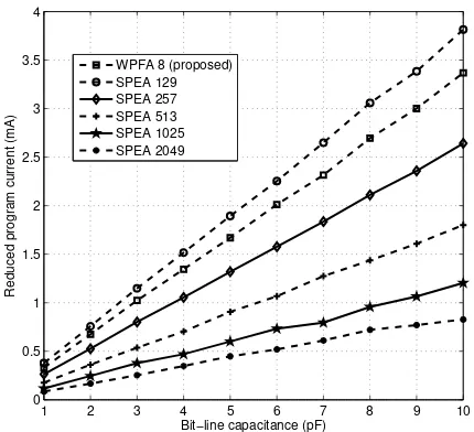
The average page-programming current is calculated when 16 blocks data are written to the memory systems. The reduced program current over the reference system as the bit-line capacitance increases is shown in Fig. 4. In this experiment, the data unit length is set to 8 and NT H of SPEA is set to 6.
It has been observed that in terms of energy consumption, the system employed with WPFA outperforms the system employed with SPEA whose codeword is larger than 257 bits. Since the large codeword is generally used in SPEA to reduce flag overhead, WPFA will typically be advantageous.
C. Proportion of the Highest Vth State
To theoretically analyze the proportion of NAND cells on the highest Vth state, it is necessary to derive the amount of
1’s in lower pages (or 0’s in upper pages) of programming data, which is calculated in the following way.
All possible input patterns are divided into two groups: A and B, by the MSB of the sum register, as shown in Fig. 5. For group A with MSB=0, the second stage of the algorithm
1 2 3 4 5 6 7 8 9 10
0 0.5 1 1.5 2 2.5 3 3.5 4
Bit−line capacitance (pF)
Reduced program current (mA)
[image:4.612.327.542.67.263.2]WPFA 8 (proposed) SPEA 129 SPEA 257 SPEA 513 SPEA 1025 SPEA 2049
Fig. 4: Reduced program current over the system without power saving scheme
User data length: 2N bits
k: Number of Ā1ās
Number of patterns
Number of Ā1ās after precoding Flag 0 1 N-1 N N+1 2N-1 2N 0 2N C 1 2N C N -1 2N C N+1 2N C N 2N C 2N 2N C 2N-1 2N C
Ā0ā Ā0ā
Ā0ā
Ā1ā Ā1ā
[image:4.612.311.554.319.472.2]Ā1ā Ā0ā 2N-0 2N-1 2N-(N-1) 2N-2N Group A: All flip Group B: Half flip
Fig. 5: Data patterns before and after WPFA processing
is performed and the number of 1’s (with flag bits) is given by
NA
1 =
NX1
k=0
C2kN(2N k) (2)
whereCk
nis the binomial coefficientCnk =k!(n kn! )!. For group
B with MSB=1, the first stage of the algorithm is performed and only half of the bits are flipped. It is not possible to exactly determine the number of 1’s for each individual data pattern, which is the reason it is not shown in Fig. 5. Nonetheless, the total number of 1’s after processing can still be calculated taking advantage of symmetry. If we think of the number of 1’s related to flags, the total number of 1’s in group B after WPFA processing is expressed as
NB
1 =
2XN 1
k=N
C2kN(2N)
1 2
2XN 1
k=N
C2kN(k) +
2NX1
k=N
C2kN (3)
Since the total number of data patterns is22N⇥(2N+ 1), the
4
0.5 0.52 0.54 0.56 0.58 0.6 0.62 0.64 0.66 0.68 0.7
23 24 25 26 27 28 29 Data unit length
Probability of 1s
[image:5.612.63.276.67.254.2]Asymmetric coding WPFA (simulated) WPFA (theoretical)
Fig. 6: Simulation results of probabilities of “1”s in Tanaka-maru’s and the proposed schemes
of 1’s in all data patterns with flag bits by 22N ⇥(2N+ 1),
which is
P1= N
A
1 +NB1
22N ⇥(2N+ 1)
=
2NP1
k=N
Ck
2N(N+ 1) +
NP1
k=0
Ck
2N(2N k)
22N ⇥(2N+ 1)
(4)
Note that for the flag bits, we could choose either 1 or 0 for the specific group; however, setting the flag bits of group B to be 1 can increase the probability of 1’s of the output bit stream, and the condition is adverse for the upper pages.
In computer simulations, we measured the probability of 1’s of lower pages data for both asymmetric and WPFA encoder, as illustrated in Fig. 6. When the length of input data is large enough, the simulated probability of 1’s for WPFA is fairly close to its theoretical counterpart. Performance loss has been observed in the proposed design comparing to asymmetric coding because of the half-flip operations. At the unit length of 24, this loss is about 5% in the target of 1’s probability.
However, the performance gap between these two schemes gets smaller when the data unit length increases. In the design of SSD systems, if we set the data unit length to be 24,
the WPFA will modify the data programmed to NAND so that at least 55% of the lower and upper pages are 1’s and 0’s, respectively. As a result, the highest Vth state, “10”
occupies 20% of the total data, which has been reduced by 20% compared to randomized interleaving.
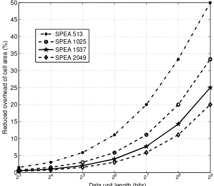
D. Overhead of NAND Cell Area
Due to the fact that extra flag bits have to be used for SPEA while the proposed scheme shares only one flag bit for both realizations, Tanakamaru’s design consumes more NAND cell area. Fig. 7 depicts the reduced overhead of the system employed with WPFA compared to three systems employed
0 5 10 15 20 25 30 35 40 45 50
23 24 25 26 27 28 29
Data unit length (bits)
Reduced overhead of cell area (%)
[image:5.612.328.541.69.254.2]SPEA 513 SPEA 1025 SPEA 1537 SPEA 2049
Fig. 7: The reduced NAND cell area overhead to Tanakamaru’s design
WPFA Encoder
ECC Encoder
MLC NAND Flash Memory
Array
ECC Decoder
WPFA Decoder
[image:5.612.304.563.306.357.2](FPGA) (FPGA)
Fig. 8: Framework of coding mechanism in SSDs
with same asymmetric coding and different length of SPEA codeword. It is seen that the reduced overhead increases with data unit length and Tanakamaru’s design consumes even more cell area when the codeword of SPEA gets shorter. For 256-bit data unit and 1025-bit SPEA codeword, the extra cell area of Tanakamaru’s design has been reduced as much as20%.
IV. HARDWAREDESIGN ANDIMPLEMENTATION
COMPLEXITY
d0 d1
d0 d1 d14
data input
modified data of input data
MSB
d14 d15
d16
d15
4bit adder
[image:6.612.74.273.59.287.2]U/L U/L = 1 lower page data U/L = 0 upper page data
[image:6.612.49.306.343.421.2]Fig. 9: Circuit schematic of the joint lower/upper pages coding
TABLE I: Comparisons of FPGA Resource Utilization
Encoding Units ALUTs Registers Packed ALMs
Asymmetric (len = 16) 81 34 43
SPEA (len = 129,NT H= 6) 357 150 183
SPEA (len = 257,NT H = 6) 717 281 364
SPEA (len = 513,NT H= 6) 1432 540 727
SPEA (len = 1025,NT H= 6) 2828 1055 1433
WPFA (len = 16) 38 17 19
be correspondingly produced when the flash controller fetches data from the memory array. Hence, in the decoding side, the decoder circuit is easy to implement by performing XOR operations over the input data, the flags and the U/L signal. Due to the fully combinational circuits, the latency, circuit area, and logic resources related to WPFA are small. To quantitatively depict the complexity of each computation unit, we used Verilog to model the proposed circuits. The encoding units were synthesized with Synplify Pro and Altera EP2S180 FPGA according to area optimization. The adaptive look-up tables (ALUTs) and logic registers utilized for each encoding unit are listed in Table I. Results for Tanakamaru’s design are included for comparison. In this experiment, the same serial/parallel conversion circuits were assumed for either design thus we only need to compare the complexity of the computation units. As seen, WPFA requires much less logic resources than that of asymmetric coding and SPEA, especially when the code length of SPEA increases. Even compared to the design employed with asymmetric coding only, WPFA still shows lower complexity. The estimated adaptive logic modules (ALMs) used for WPFA encoder is about 8% of the ALMs consumed by Tanakamaru’s design for code length of 129 and NT H of 6 for SPEA. The resource utilization of Tanakamaru’s
design should be double if considering both lower and upper pages whereas that of the proposed design stays the same.
V. CONCLUSIONS
In this paper, we present a write pattern formatting algo-rithm of low complexity to improve the data retention relia-bility and power consumption of NAND flash based SSDs. The proposed algorithm improves on the existing SPEA approach to completely eliminate column stripe patterns. Furthermore, simulation results show that the overhead for the proposed algorithm is about 80% compared to SPEA using the same parameters. Finally, hardware synthesized results over Altera EP2S180 demonstrate that the implementation complexity of the proposed scheme is much less than that of asymmetric coding and SPEA.
REFERENCES
[1] G. Dong, S. Li, and T. Zhang, “Using Data Postcompensa-tion and PredistorPostcompensa-tion to Tolerate Cell-to-Cell Interference in MLC nand Flash Memory,”IEEE Trans. Circuits Syst. I, Reg. Papers, vol. 57, no. 10, pp. 2718–2728, Oct 2010. [2] S. Tanakamaru, C. Hung, A. Esumi, M. Ito, K. Li, and K. Takeuchi, “95%-lower-BER 43%-lower-power Intelli-gent Solid-State Drive (SSD) with Asymmetric Coding and Stripe Pattern Elimination Algorithm,” in IEEE Int. Solid-State Circuits Conf. (ISSCC), Feb 2011, pp. 204– 206.
[3] R. Micheloni, L. Crippa, and A. Marelli, “Inside NAND Flash Memories,”Springer Press, Aug 2010.
[4] S. Tanakamaru, C. Hung, and K. Takeuchi, “Highly Reli-able and Low Power SSD Using Asymmetric Coding and Stripe Bitline-Pattern Elimination Programming,”IEEE J. Solid-State Circuits, vol. 47, no. 1, pp. 85–96, Jan 2012. [5] Y.-P. Hu, N. Xiao, and X.-F. Liu, “An elastic error
correc-tion code technique for NAND flash-based consumer elec-tronic devices,” IEEE Trans. Consum. Electron., vol. 59, no. 1, pp. 1–8, Feb 2013.
[6] K. Takeuchi, “Novel Co-Design of NAND Flash Memory and NAND Flash Controller Circuits for Sub-30 nm Low-Power High-Speed Solid-State Drives (SSD),” IEEE J. Solid-State Circuits, vol. 44, no. 4, pp. 1227–1234, 2009. [7] K.-D. Suh, B.-H. Suh, and Y.-H. Lim, “A 3.3 V 32 Mb NAND Flash Memory with Incremental Step Pulse Pro-gramming Scheme,”IEEE J. Solid-State Circuits, vol. 30, no. 11, pp. 1149–1156, Nov 1995.
[8] K. Fukuda, Y. Watanabe, E. Makino, K. Kawakami, J. Sato, T. Takagiwa, N. Kanagawa, H. Shiga, N. Tokiwa,
and Y. Shindo, “A 151-mm2 64-Gb 2 Bit/Cell NAND
Flash Memory in 24-nm CMOS Technology,” IEEE J.