International Journal of Innovative Technology and Exploring Engineering (IJITEE)
ISSN: 2278-3075, Volume-8 Issue-12, October 2019
Abstract: Multiband reconfigurable patch antenna plays a vital role in wireless communication applications. By changing the current path on the patch a multiband reconfigurable antenna can be achieved. A simple multiband frequency reconfigurable microstrip patch antenna is presented in this paper. The proposed antenna structure is simulated in CST microwave studio. This antenna operates between 1.3 to 5.6 GHz with more than fifteen different frequencies. The antenna is analyzed for four different configurations. The designed antenna is resonating at five different frequencies (1.45 GHz, 2.36 GHz, 3.09 GHz, 3.6 GHz and 5.45 GHz) when both PIN diodes are ON. When PIN diode D1 is ON and D2 is OFF the antenna is resonating at 1.4 GHz, 2.22 GHz, 2.5 GHz, 3.08 GHz and 3.59 GHz. When D1 is OFF and D2 is ON the antenna is resonating at 2.34 GHz, 3.2 GHz, 3.62 GHz and 5.38 GHz frequencies. The slotted antenna or when both PIN diodes are in OFF condition antenna is resonating at 2.22 GHz, 2.49 GHz, 3.21 GHz, 3.6 GHz and 5.42 GHz. For each configuration the antenna parameters like gain, VSWR, directivity and radiation patterns are analyzed.
Keywords: Multiband,PIN Diodes, Frequency Reconfigurable antenna, CST MWS
I.
INTRODUCTION
T
he disadvantages of conventional antenna can be
overcome by using reconfigurable antenna where we can
dynamically alter the antenna parameters like radiation
pattern, operating frequency, polarization or combination of
these parameters which is not possible with the conventional
antenna [1] [12]. Day by day the demand for wide band,
multiband reconfigurable antenna is increasing which satisfy
wireless communication applications. For satellite and
wireless communication applications the reconfigurability
feature has become an essential component of modern,
radio-frequency (RF) systems [3] [5]. The cost of
communication systems, size and complexity can be
significantly reduced by using reconfigurable antenna
technique. Switching devices like PIN diodes, varactor diodes
or MEMS switches are used to change the current paths on the
antenna thereby we can achieve multi frequency function [2]
[6]. The designed antenna contains two slots, one slot on
Revised Manuscript Received on October 05, 2019. * Correspondence Author
Rajendra Soloni*, Department of E&CE, GM Institute of Technology, Davangere, Davangere, India. Email: rajendrass@gmit.ac.in
Rajappa H S, Department of E&CE, GM Institute of Technology, Davangere, Davangere, India. Email: rajappahs@gmit.ac.in
Chandrappa D N, Department of E&CE, PESITM, Shivamogga, Shivamogga, India. Email: chandrappadn@pestrust.edu.in
patch and other one on ground surface. PIN diode is placed in
patch slot as well as ground slot. The effect of switching
effects, gain, directivity, VSWR and radiation patterns are
discussed.
II.
ANTENNA
GEOMETRY
CST microwave studio is used to design and simulate the
proposed antenna. The structure of the antenna is shown in
fig.1 (front view) and fig. 2 (back view). FR-4 lossy (with
dielectric constant of 4.3) is used as the substrate material and
the height is 1.6 mm. The dimension of the patch is 46.07 mm
X 35.85 mm. Frequency reconfigurability is achieved by
using two PIN diodes (BAP50_02). Following formulae [7],
[12] were used to design the antenna:
Width of the patch can be calculated by,
Length of the patch can be calculated by,
Where
Design and Analysis of Frequency
Reconfigurable Microstrip Patch antenna for
Multi Band Operations using PIN Diodes
using PIN Diodes
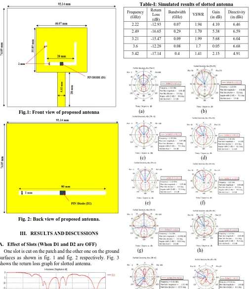
Fig.1: Front view of proposed antenna
Fig. 2: Back view of proposed antenna.
III.
RESULTS
AND
DISCUSSIONS
A.
Effect of Slots (When D1 and D2 are OFF)
One slot is cut on the patch and the other one on the ground
surfaces as shown in fig. 1 and fig. 2 respectively. Fig. 3
shows the return loss graph for slotted antenna.
[image:2.595.49.555.48.632.2]Fig. 3: Return Loss graph of Slotted antenna
Simulated results of slotted antenna are presented in
Table-I.
Table-I: Simulated results of slotted antenna
Frequency(GHz)
Return Loss (dB)
Bandwidth
(GHz) VSWR
Gain (in dB)
Directivity (in dBi)
2.22 -12.93 0.07 1.94 4.10 6.46
2.49 -16.65 0.29 1.70 5.38 6.59
3.21 -15.47 0.09 1.99 5.68 6.04
3.6 -12.28 0.08 1.7 0.05 6.68
5.42 -17.14 0.4 1.41 2.15 4.91
(a) (b)
(c) (d)
(e) (f)
(g) (h)
[image:2.595.288.548.76.665.2](i) (j)
Fig. 4: Radiation patterns for slotted antenna. [(a), (c),
(e), (g) and (i) represent E-plane] and [(b), (d), (f), (h) and
(j) represent H-plane]
[image:2.595.50.287.593.723.2]International Journal of Innovative Technology and Exploring Engineering (IJITEE)
ISSN: 2278-3075, Volume-8 Issue-12, October 2019
The slotted antenna can be used for Mobile Satellite
Service, Broadband Radio Service, TV Broadcast Auxiliary
Service, Amateur Radio Service, the Fixed Satellite Service,
Radiolocation
Service
and
Long-distance
radio
telecommunications.
B.
B. Effect of PIN Diode
i.
Case-I: Both PIN diodes (D1 and D2) are ON:
To achieve the frequency reconfigurability one PIN Diode is
placed in the patch slot as shown in the fig. 1 and other is
placed in the ground slot as shown in fig. 2. Table-II presents
the simulated results of the proposed antenna when PIN diode
D1 and PIN diode D2 are in ON condition. The antenna
radiates at 1.4 to 5.5 GHz as shown in fig. 5.
[image:3.595.312.542.49.228.2]Fig. 5. Return Loss graph for proposed antenna (Case-I)
Table-II: Simulated results for Case-I
Frequency (GHz)
Return Loss (dB)
Bandwidth
(GHz) VSWR
Gain (in dB)
Directivity (in dBi)
1.45 -40.8 0.313 1.27 2.41 4.04
2.36 -19.27 0.458 1.67 5.15 6.36
3.09 -22.85 0.203 1.72 5.78 8.31
3.6 -21.95 0.09 1.70 0.05 6.68
5.45 -13.79 0.43 1.45 2.31 5
The simulated radiation patterns are presented in fig. 6.
(a) (b)
(c) (d)
(e) (f)
(g) (h)
[image:3.595.50.565.342.815.2](i) (j)
Fig. 6: Radiation patterns for Case-I. [(a), (c), (e), (g) and
(i) represent E-plane] and [(b), (d), (f), (h) and (j)
represent H-plane].
This antenna configuration can be used for Aviation Service,
Maritime Service, Radiolocation Service, Fixed Satellite
Service and long-distance radio telecommunications.
ii.
Case-II: D1 ON and D2 OFF:
For case-II the configuration is PIN diode D1 is ON and D2
is OFF. For this configuration antenna radiates at 1.4 to 3.59
GHz, which is shown in fig.7. Table-III presents the simulated
results for case-ii configuration and radiation patterns are
shown in fig. 8.
Fig. 7. Return Loss graph for proposed antenna (Case-II)
Table-III: Simulated results for Case-II
Frequency(GHz)
Return Loss (dB)
Bandwidth
(GHz) VSWR
Gain (in dB)
Directivity (in dBi)
1.4 -30.33 0.18 1.3 2.25 3.96
2.22 -14.48 0.09 1.94 4.10 6.46
2.5 -17.08 0.29 1.71 5.41 6.61
3.08 -40.70 0.18 1.70 5.78 8.28
3.59 -16.82 0.08 1.84 -0.25 6.57
[image:3.595.302.557.390.491.2]using PIN Diodes
(c) (d)
(e) (f)
(g) (h)
[image:4.595.299.532.47.379.2](i) (j)
Fig. 8: Radiation patterns for Case-II. [(a), (c), (e), (g) and
(i) represent E-plane] and [(b), (d), (f), (h) and (j)
represent H-plane].
This antenna configuration can be used for Earth
Exploration-Satellite, Radio Astronomy, and Space Research
Services, Broadband Radio Service, Mobile Satellite Service,
TV Broadcast Auxiliary, Maritime Service, Fixed Satellite
Service and the Radiolocation Service.
iii. Case-III: D1 OFF and D2 ON:
When PIN diode D1 is OFF and PIN diode D2 is ON the
antenna radiates at 2.34 GHz to 5.38 GHz as shown in fig.9.
Table-IV presents the simulated results of Case-III and
radiation patterns are shown in fig. 10.
Fig. 9. Return Loss Graph for Case-III.
Table-IV: Simulated results for Case-III
Frequency(GHz)
Return Loss (dB)
Bandwidth
(GHz) VSWR
Gain (in dB)
Directivity (in dBi)
2.34 -18.52 0.41 1.66 5.06 6.18
3.2 -27.22 0.10 2.02 5.71 6.04
3.62 -37.21 0.10 1.49 0.83 6.98
5.38 -14.48 0.44 1.38 1.78 4.09
(a) (b)
(c) (d)
(e) (f)
(g) (h)
Fig. 10: Radiation patterns when D1 is ON and D2 is
OFF. [(a), (c), (e) and (g) represent E-plane] and [(b), (d),
(f) and (h) represent H-plane].
This antenna configuration can be used for Aviation Service
and the Wireless Communications Service, Amateur Radio
Service, the Fixed Satellite Service, Radiolocation Service
and long-distance radio telecommunications.
iv. Case-III: Both D1 and D2 OFF:
When both the PIN diodes are off the antenna configuration
is similar to the slotted antenna which is discussed in section
III A.
[image:4.595.61.321.48.379.2]A comparison between proposed antenna with different
antenna models available in literature is presented in Table-V.
Table-V: Comparison results
Reference
No. of PIN diodes
used
Patch Area (WxL) mm2
Resonant Frequencies (GHz)
Reconfigurable Single and Dual Band Microstrip Patch Antenna for
Satellite communications [8]
4 17.4x12.48 3.46, 3.99,
and 4.64
Design frequency reconfigurable Microstrip patch antenna for s-band
Applications [9]
[image:4.595.45.554.554.807.2]International Journal of Innovative Technology and Exploring Engineering (IJITEE)
ISSN: 2278-3075, Volume-8 Issue-12, October 2019
Design of Reconfigurable Fractal Antenna
using Pin Diode Switch for
Wireless Applications [10]
6 30x30
2.47, 3.58, 3.62, 5.55, 5.88, 5.93, 6, 6.07,8.63, 8.67 and 8.72
Frequency Reconfigurable
Rectangular Antenna with
TSlotted Feed Line [11]
2 98.5x72 1.8, 2.3 and 2.4
Proposed 2 46.07X35.85
1.4, 1.45, 2.22, 2.34, 2.36, 2.49,
2.5, 3.08, 3.09, 3.2, 3.21, 3.59, 3.6, 3.62, 5.38, 5.42, and 5.49
IV.
CONCLUSION
CST MWS tool is used to design and analysis of multiband
frequency reconfigurable antenna. Only two PIN diodes have
been used to configure the antenna as multiband frequency
reconfigurable antenna. Four different configurations are
presented for the proposed antenna. This antenna operates
between 1.3 to 5.6 GHz with more than fifteen different
frequencies. A comparison results of proposed antenna were
discussed. The antenna is compact, low cost, has high gain
and directivity, low power and it will be well suited for L
band, S band, and C-band wireless applications.
REFERENCES
1. M. F. Ismail, M. K. A. Rahim and H. A. Majid, "The Investigation of PIN diode switch on reconfigurable antenna," RF and Microwave Conference (RFM), 2011 IEEE International, Seremban, Negeri Sembilan, 2011, pp. 234-237.
2. J. H. Kim and C. G. Christodoulou, "A simple reconfigurable microstrip antenna for wideband applications," 2010 IEEE Antennas and Propagation Society International Symposium, Toronto, ON, 2010, pp. 1-4.
3. Christodoulou, C.G.; Tawk, Y.; Lane, S.A.; Erwin, S.R., "Reconfigurable Antennas for Wireless and Space Applications," Proceedings of the IEEE, vol.100, no.7, pp.2250, 2261, July 2012 4. Chandrappa D.N., Mrs.Vani R.M. and P.V. Hunagund “Design and
Implementation of Slotted Reconfigurable Microstrip Antenna for Wireless Application”, International Journal of Electronics and Communication Engineering. ISSN 0974-2166 Volume 6, Number 3 (2013), pp. 233-239
5. P. Sarah, K. Venkateswarlu, K. Satish Reddy, K. Praveen Kumar, P. Bhaskara Reddy, Harswaroop Vaish, 2nd International Conference on Nanomaterials and Technologies (CNT 2014) Novel Frequency Reconfigurable Slotted Patch Antenna: Design and Analysis, Procedia Materials Science, Volume 10, 2015, Pages 660-665.
6. R. J. Chitra and V. Nagarajan, "Frequency reconfigurable antenna using PIN diodes," Communications (NCC), 2014 Twentieth National Conference on, Kanpur, 2014, pp. 1-4.
7. C.A. Balanis, Antenna Theory Analysis and Design, Third Edition, New Jersey: J. Wiley & Sons, 2005
8. R. Yadav, S. K. Yadav and I. B. Sharma, "Reconfigurable single and dual band microstrip patch antenna for satellite communications," 2015 International Conference on Green Computing and Internet of Things (ICGCIoT), Noida, 2015, pp. 1565-1570.
9. B. l. Sharma, G. Parmar and M. Kumar, "Design of frequency reconfigurable microstrip patch antenna for S-Band and C-Band applications," 2015 4th International Conference on Reliability, Infocom Technologies and Optimization (ICRITO) (Trends and Future Directions), Noida, 2015, pp. 1-3.
10. Y. B. Chaouche, F. Bouttout, I. Messaoudene, L. Pichon, M. Belazzoug and F. Chetouah, "Design of reconfigurable fractal antenna using pin diode switch for wireless applications," 2016 16th
Mediterranean Microwave Symposium (MMS), Abu Dhabi, 2016, pp. 1-4.
11. T. Sabapathy, M. A. Bashah, M. Jusoh, P. J. Soh and M. R. Kamarudin, "Frequency reconfigurable rectangular antenna with T-slotted feed line," 2016 International Conference on Radar, Antenna, Microwave, Electronics, and Telecommunications (ICRAMET), Jakarta, 2016, pp. 81-84.
12. R. Soloni, H. S. Rajappa and D. N. Chandrappa, "Design and analysis of multiband reconfigurable microstrip patch antenna with switchable element," 2017 International Conference on Advances in Computing,
Communications and Informatics
(ICACCI), Udupi, 2017, pp. 288-293.
AUTHORS
PROFILE
Rajendra Soloni has completed his B.E in E&CE discipline at SDMCET, Dharwad
and M. Tech in Digital Electronics at BVBCET, Hubli. He is currently working as an Assistant Professor in Department of E&CE at GM Institute of Technology, Davangere, Karnataka. He is a life member of ISTE. His area of interest includes reconfigurable microstrip patch antennas, Wireless Communication, microwaves and Digital Signal Processing.
Rajappa H S has completed his B.E in E&CE discipline at SDMCET, Dharwad and M. Tech in Digital Electronics at BVBCET, Hubli. He is currently working as an Assistant Professor in Department of E&CE at GM Institute of Technology, Davangere, Karnataka. He is a life member of ISTE. His area of interest includes wireless communication, ultra
wideband antennas, miniaturized
microstrip patch antennas and analog electronics
Chandrappa. D. N has obtained his Ph.D from Gulberga University in the area of microstrip patch antenna. Completed his M. Tech in Digital Communication & Networking at Davangere University and B.E in Electronics and communication discipline at Kuvempu University and. He has published 10 international journals and attended more than ten national and international conference. He is a life member of ISTE. He is currently working as a Professor and Head in Department of
Electronics and Communication
Engineering at PES Institute of technology
and Management, Shivamogga,
![Fig. 6: Radiation patterns for Case-I. [(a), (c), (e), (g) and (i) represent E-plane] and [(b), (d), (f), (h) and (j) represent H-plane]](https://thumb-us.123doks.com/thumbv2/123dok_us/8171492.252072/3.595.302.557.390.491/fig-radiation-patterns-case-represent-plane-represent-plane.webp)
![Fig. 8: Radiation patterns for Case-II. [(a), (c), (e), (g) and (i) represent E-plane] and [(b), (d), (f), (h) and (j)](https://thumb-us.123doks.com/thumbv2/123dok_us/8171492.252072/4.595.61.321.48.379/fig-radiation-patterns-case-ii-represent-e-plane.webp)
