1-1-1990
Interfacing a single-board computer to a digital
voice recorder for use in developing a speech
recognition system
Gary A. Fagan
Iowa State University
Follow this and additional works at:https://lib.dr.iastate.edu/rtd Part of theEngineering Commons
This Thesis is brought to you for free and open access by the Iowa State University Capstones, Theses and Dissertations at Iowa State University Digital Repository. It has been accepted for inclusion in Retrospective Theses and Dissertations by an authorized administrator of Iowa State University Digital Repository. For more information, please [email protected].
Recommended Citation
Fagan, Gary A., "Interfacing a single-board computer to a digital voice recorder for use in developing a speech recognition system" (1990).Retrospective Theses and Dissertations. 18386.
..£~/
/
7'/#
F/.31
(! • ~
speech recognition system
by
Gary A. Fagan
A Thesis Submitted to the
Graduate Faculty in Partial Fulfillment of the Requirements for the Degree of
MASTER OF SCIENCE
Interdepartmental Program: Major:
Signatures have been redacted for privacy
Biomedical Engineering Biomedical Engineering
Iowa State University Ames, Iowa
TABLE OF CONTENTS
DEDICATION INTRODUCTION
A COMPUTER-CONTROLLED DIGITAL RECORDER The Digital Voice Module
The T6668 microprocessor Microphone amplifier
ADM analysis/ synthesis circuit D-RAM I / F
Address counter
Stop address register Index register
Refresh counter
Timing generator control circuit D/ A converter/voltage follower Bandpass filter
CPU I / F
Status register Audio circuit
Power circuit Memory
Control switches DIP switch
Push-button switches The MC-lZ Single-Board Computer
The Zilog Z8671 microcomputer BASIC/ DEBUG interpreter Ports 2 and 3
viii 1 3 3 4 5 5 10 10 10 10 10 12 13 13 13 15 18 19 19 21 21 21 23 23 26 27 The 8255A programmable peripheral interface (PPI} 29
The MM58 274 clock/ calendar 31
2K/ 8K RAM socket 31
The MC-lZ application socket 33
Power supply module
Negative voltage generator Interfacing the DVM-1 to the MC-lZ
DVM-1 alterations The interface circuit Software
Label/Index mode Direct mode
Firmware
SPEECH RECOGNITION Literature Review
Problems
Ambiguities of speech
Variations in pronunciation Categories
The speech recognition process Speech sound production Speech signal acquisition Speech signal analysis
Speech recognition algorithms Aids for the disabled
Deafness and hearing impairments Motor impairments
Speech impairments Speech Recognition Systems
Literature review The Z-80 system The 6502 system The Z8671/ DVM-1 system
Speech data acquisition Software
RESULTS AND RECOMMENDATIONS
BIBLIOGRAPHY ACKNOWLEDGEMENTS
APPENDIX A: T6668 PIN CONNECTIONS
APPENDIX B: A SAMPLE PROGRAM FOR RECORDING IN THE LABEL/INDEX MODE
APPENDIX C: A SAMPLE PROGRAM FOR RECORDING IN THE DIRECT MODE
65
67
68
69
70
LIST OF FIGURES
Figure 1. Top view of the Digital Voice Module with the main components labeled: {A) T6668
speech microprocessor, (B) Memory, (C) Control switches, (D) Power circuit, (E) Audio circuit,
(F) Volume control, (G) Microphone jack,
(H) Speaker jack, and (I) Power jack 3
Figure 2. Block diagram of the T6668 showing the functional components (Toshiba America,
Inc., 1988) 4
Figure 3. The equivalent circuits of the two
micro-phone amplifiers of the T6668 (Toshiba
America, Inc., 1988) 5
Figure 4. Connections between the microphone and the T6668 to achieve the third amplifier
configuration (Toshiba America, Inc., 1988) 6
Figure 5. An example of pulse code modulation showing sampling, quantization, and binary encoding
(Feher, 1987) 7
Figure 6. Quantization noise in linear delta
modulation (Feher, 1987) 9
Figure 7. Quantization noise in adaptive delta
modulation (Feher, 1987) 9
Figure 8. Connection of D-RAM to the T6668 (Toshiba
America, Inc. , 1988) 11
Figure 9. Equivalent circuit of the bandpass filter
(Toshiba America, Inc., 1988) 14
Figure 10. The T6668 wired for the manual mode
(Toshiba America, Inc., 1988) 16
Figure 11. The T6668 used in the CPU mode (Toshiba
America, Inc. , 1988) 17
Figure 12. The audio circuit and its connection to
the T6668 19
Figure 13. Pin diagram and nomenclature for a 256
Kbit D-RAM (Texas Instruments, Inc., 1984) 20
Figure 15. Memory map of the MC-lZ
Figure 16. Block diagram of the Z8671 (Zilog, Inc., 1984)
Figure 17. The Port 2 mode register (Zilog, Inc., 1984)
Figure 18. The control register for setting ports A, B, and C for input and/ or output
(Uffenbeck, 1985) Figure 19.
Figure 20. Figure 21.
Figure 22.
Figure 23.
Figure 24.
Circuit alterations of the DVM-1 board The interface circuit
Anatomy of the human vocal tract (Hollingum , 1988)
A speech spectrum showing the formants (Cater, 1984)
Process of a Fast-Fourier Transform (Bristow, 1984)
A spectrogram consisting of a series of FFTs (Cater, 1984)
25
26
29
30 37 39
49
50
53
LIST OF TABLES
Table 1. Three possible amplifier configurations using the two available T6668 microphone
amplifiers 6
Table 2. Logic levels of Ml and M2 based on the number of D-RAMs used (Toshiba America,
Inc., 1988) 12
Table 3.
Table 4.
Table 5.
Table 6 .
Table 7.
Table 8. Table 9.
Table 10.
Table 11. Table 12.
Designation of status register bits
(Toshiba America, Inc., 1988) 18
Selection of recording bit rate using
switches 1 and 2 21
Designation of phrase number using
switches 3, 4, 5, and 6 22
Indication of the number of D-RAMs
installed based on switch 7 and 8 settings 22
Relational operators supported by BASIC/
DEBUG (Zilog, Inc., 1981) 27
Commands recognized by BASIC/DEBUG 28
Possible I / O combinations for ports A, B,
and C (Basicon, Inc., 1984) 31
Clock counters and their addresses and
modes (Basicon, Inc., 1984) 32
T6668 commands (Toshiba America, Inc ., 1988) 40
Function, port value, and command statement for each step of the recording process in
the Label/Index mode 42
Table 13. Commands offered by the MC-lZ utility PROM 45
Table 14. Formant resonances of vowel sounds (Cater,
DEDICATION
INTRODUCTION
The purpose of this project was to develop a computer-controlled digital voice recorder by interfacing a digital voice recorder to a single-board computer for use in a
biomedical application. The single-board computer is the MC-lZ by Basicon, Inc., and the digital voice recorder is the Digital Voice Module (DVM-1) by Ming Engineering & Products, Inc.
The MC-lZ is a low-cost, portable microcontroller that can be programmed in BASIC and/ or machine language. Once the MC-lZ is supplied with +5 Vdc power and connected to an RS-232 compatible terminal, it is ready to be programmed for many control applications.
The DVM-1 is one of several digital voice recorders
available on the market today. These recorders are similar in operation to audio cassette recorders except that they store voice data in memory integrated circuits (chips) instead of using magnetic tape. The advantages of memory chips are that they last longer than tape and allow more convenient access to voice data. The disadvantage is that the memory chips used in this project must be constantly powered to maintain storage of the voice data.
obvious application of the speech recognizer is verbal control of the MC-lZ. This capability would allow a person, unable to type on a keyboard, to operate and program the MC-lZ computer.
The implementation of the MC-lZ/ DVM-1 speech recognition system is described in this thesis. The first section
provides information on the components and operation of the DVM-1 recorder and the MC-lZ computer and explains the
hardware and software used in interfacing the recorder and the computer. Additional hardware and software information is
given Appendices A, B, and
c.
The second section gives an overview of speech
A COMPUTER-CONTROLLED DIGITAL RECORDER
The Digital Voice Module
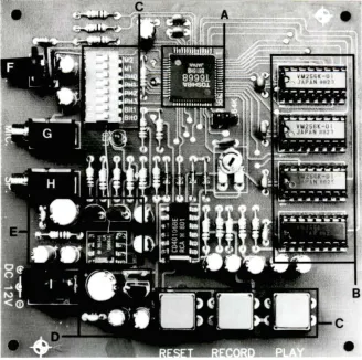
The main components of the DVM-1 are labeled in Figure 1 .
Figure 1. Top view of the Digital Voice Module with the main components labeled: {A) T6668 speech
microprocessor, (B) Memory, (C) Control switches, (D) Power circuit, (E) Audio circuit, {F) Volume control, (G) Microphone jack, (H) Speaker jack, and
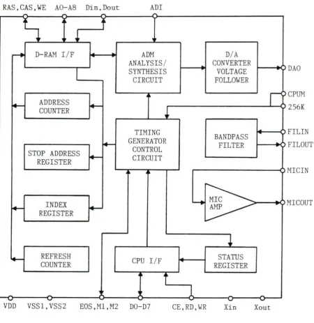
[image:12.568.107.435.234.560.2]The T6668 microprocessor
The T6668 consists of several functional components shown in Figure 2. The pin connections are shown in Appendix A.
RAS,CAS ,WE A0-A8 Din,Dout
ADI
-
,..~
'.
f
[image:13.562.52.503.171.635.2]••
l
...
...
D-RAM I/F
---
.ADM
ANALYSIS/
I
SYNTHESIS
CIRCUIT
• i
ADDRESS
I+-~
COUNTER
~
TIMING
+-
GENERATOR
STOP ADDRESS
CONTROL
REGISTER
+-
CIRCUIT
0 ~
INDEX
I+-
REGISTER
I+-14-
REFRESH
COUNTER
CPU I/F
.~
t
...
•
- ...
-VDD VSS1, VSS2
EOS,Ml,M2 D0-07
DIA
-
CONVERTER
.
VOLTAGE
FOLLOWER
BANDPASS
FILTER
-~
~
l
-
STATUS
-
REGISTER
1
-CE , RD , WR
Xin
-r ..
-'""' l
-
~-.
""Xout
DAO
CPUM
256KFIL IN
FI LOUT
MICIN
MICOUT
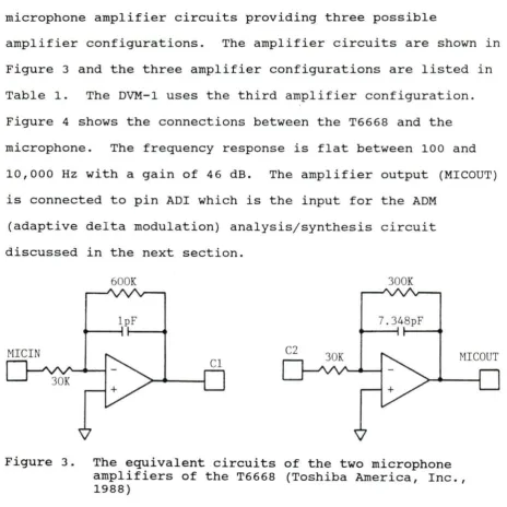
Microphone amplifier The T6668 includes two microphone amplifier circuits providing three possible
amplifier configurations. The amplifier circuits are shown in Figure 3 and the three amplifier configurations are listed in Table 1. The DVM-1 uses the third amplifier configuration. Figure 4 shows the connections between the T6668 and the microphone. The frequency response is flat between 100 and 10,000 Hz with a gain of 46 dB. The amplifier output (MICOUT) is connected to pin ADI which is the input for the ADM
(adaptive delta modulation) analysis/ synthesis circuit discussed in the next section.
600K 300K
lpF 7. 348pF
Figure 3. The equivalent circuits of the two microphone amplifiers of the T6668 (Toshiba America, Inc., 1988)
ADM analysis/synthesis circuit The ADM analysis/
synthesis circuit receives the amplified microphone signal at pin ADI. The function of this circuit is to convert the
[image:14.568.49.514.109.574.2]conversion include pulse code modulation (PCM), differential pulse code modulation (DPCM), and delta modulation (DM) which
includes linear delta modulation (LDM) and adaptive delta modulation (ADM) .
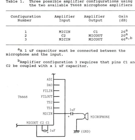
Table 1. Three possible amplifier configurations using the two available T6668 microphone amplifiers
Configuration Amplifier Amplifier Gain
Number Input Output (dB)
1 MIC IN Cl 26a
2 C2 MICOUT 20a
3 MIC IN MICOUT 46a,b
aA 1 uF capacitor must be connected between the microphone and the input.
bAmplifier configuration 3 requires that pins Cl a nd C2 be coupled with a 1 uF capacitor.
T6668
ADI - - - . DAO
FIL IN
FI LOUT
TS2
TS l luF
MICIN - - - -+ 1----.. MICOUT C2 Cl
+ l uF (GND)
MICROPHONE
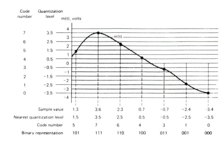
[image:15.568.71.501.205.650.2] [image:15.568.97.425.436.640.2]Pulse code modulation (PCM) Pulse code modulation involves sampling, quantization, and binary encoding of the input signal as illustrated in Figure 5 .
Code Ouantiza11on number level m(tl. volts
4 3.5 6 2.5 5 1.5
3 / / -... /
2 /
J
1
4 0.5 3 - 0.5 2 - 1.5
0 I
I
- 1 I
- 2.5 - 2 I - 3 I 0 - 3.5
- 4
I I
Sample value 1.3 3.6
Nearest quanttzatton level 1.5 3.5
Code number 5 7
Binary representation 101 1:1
[image:16.562.65.446.160.401.2]' "(t)
.,
..
... l ; : : I I 2.3 2.5 6 11 0 ... ...'"
I I I.
I' I I I I 0. 7 0.5 4 100 ...
-... ... ...,,
-
---II I I
I I
- 0. 7 -2.4 3.4 - 0.5 -2.5 - 3.5
3 0
011 001 000
Figure 5. An example of pulse code modulation showing
sampling, quantization, and binary encoding (Feher ,
1987)
Differential pulse code modulation (DPCM) Differ-ential pulse code modulation is a variation of PCM. Instead of determining a quantization level for each sample value, DPCM predicts a future sample value from the previous sample value. The difference between the predicted value and the actual value is called the prediction error. The prediction error is quantized, coded, and sent to a decoder which
reconstructs the original signal (Feher, 1987).
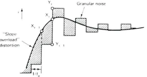
Delta modulation (OM) A version of DPCM, delta
modulation estimates the next sample value as a positive or negative increment from the previous sample value. When the increment or step size is constant (whether decreasing or increasing), delta modulation is referred to as linear
(nonadaptive) delta modulation (LDM), and when the step size can vary, it is called adaptive delta modulation (ADM).
In linear delta modulation (LDM}, the previous sample value is subtracted from the input signal. If the difference
is positive, the previous sample is increased by a step to establish the next sample value, and if the difference is negative, the previous sample value is decreased by a step
(Feher, 1987). LDM produces a signal with a maximum slope equal to the step size times the sampling rate. When the input signal exceeds this maximum slope, slope overload
(X) and the LDM signal (Y). These sources of quantization noise are illustrated in Figure 6.
Granular no ise I
Figure 6. Quantization noise in linear delta modulation (Feher, 1987)
In adaptive delta modulation (ADM), a digital algorithm is used to adapt the stepping process so that quantization noise is reduced as shown in Figure 7. Depending on the manufacturer, various algorithms are used to implement ADM, a system which provides better signal reproduction than linear delta modulation without increasing the sampling rate.
"SIOl>t' overload"
d1sto rt1on
[image:18.567.165.367.157.286.2] [image:18.567.159.394.523.646.2]D-RAM I/F The D-RAM I /F component is an interface circuit that allows the T6668 to be connected to dynamic
random access memories (D-RAMs). The T6668 accepts up to four pieces of D-RAM which may be either 64 Kbit or 256 Kbit D-RAM, but both types cannot be used together (Toshiba America, Inc., 1988). The pin connections between the T6668 and a D-RAM are shown in Figure 8. The functions of these pins will be
explained in the section concerning memory.
Address counter The address counter is a 20-bit
counter that stores the address of the current memory location in D-RAM. The value of the counter can be set or read
(Toshiba America, Inc., 1988).
Stop address register The stop address register also
has 20 bits and stores the address at which sound recording/ reproduction stops. Values may be written into the register, but they cannot be read (Toshiba America, Inc., 1988).
Index register The index register specifies the end
address of the index area. The index area in memory stores the start address, stop address, and bit rate of a recording
(Toshiba America, Inc., 1988). The user does not have direct access to this register.
Refresh counter Dynamic RAM stores information as
, " T666B -~
-
CAS4-CAS3
-NC
--
CAS2--
CASlRAS DOUT Al VDD A3 AS A7
+S Vdc WE DIN AO NC A2 A4 A6
AB
••
I
v
--
AB
vss
DIN CAS
w
DOUT ._RAS A6
AO A3
A2 A4
Al AS
VDD A7
2S6K D-RAM
11
11
O. luF GND 7/71
the D-RAM within 4 milliseconds (Toshiba America, Inc., 1988).
Timing generator control circuit The timing generator
control circuit controls the operating rate of the ADM analysis/synthesis circuit, address counter, stop address
register, and index register. Pins associated with the timing generator control circuit include EOS, Ml, M2, 256K, Xin,
Xout, and CPUM.
The EOS pin is low when recording or reproduction starts and high when recording or reproduction stops (Toshiba
America, Inc., 1988).
Pins Ml and M2 are set according to the number of D-RAMS used as indicated in Table 2.
Table 2. Logic levels of Ml and M2 based on the number of D-RAMS used (Toshiba America, Inc., 1988)
Number of D-RAMs M2 Ml
1 L L
2 L H
3 H L
4 H H
Note: His +5 volts DC and Lis ground (0 volts).
The 265K pin is set to logic low when using 64 Kbit D-RAM or logic high for 256 Kbit D-RAM (Toshiba America, Inc.,
Xin and Xout are the input and output pins of the oscillator circuit operating at 655 KHz (Toshiba America, Inc., 1988).
The T6668 can be operated in a manual control mode or a CPU control mode. The DVM-1 uses manual control; therefore, CPUM is set low. For CPU control, the CPUM pin must be set high (Toshiba America, Inc., 1988).
D/A converter/ voltage follower During voice
reproduction, voice data are retrieved from the D-RAM,
processed by the ADM analysis/ synthesis circuit, and delivered to the D/A converter/voltage follower circuit. This circuit converts the digital voice data into an analog signal made available at pin DAO. After bandpass filtering, the analog signal is sent to an audio circuit external to the T6668.
Bandpass filter The T6668 contains a bandpass filter
used during sound reproduction. The input of the bandpass filter is pin FILIN, and the output is pin FILOUT. The equivalent circuit of the filter is shown in Figure 9. The first stage is a high-pass filter, and the second stage is a low-pass filter.
CPU I/F The CPU I/F is an interface circuit that
23 . 1 8~1
ll.458pF
FIL IN
~...---i
11. 458pF
23 . lM
3. 37pF 3.37pF
4 . 718pF
23.18M
Figure 9. Equivalent circuit of the bandpass filter (Toshiba America, Inc., 1988)
Manual control Pins 00-03 are the inputs for
[image:23.569.53.510.117.483.2]available bit rates. Pin CE must be set low to record and to allow voice output at pin DAO (connected to the input of the bandpass filter). Pin WR is set high to select the recording mode, and set low for the reproduction mode (Toshiba America,
Inc., 1988). Pin RD is not used for manual mode. Connections for using the T6668 in the manual mode are shown in Figure 10.
CPU control Pins DO to D7 constitute a
bi-directional data bus used for inputting commands to the T6668 or outputting the status of the T6668. Pins CE, RD, and WR are used to determine a write operation, read operation, or neither. When CE and RD are low, the status register can be read. When CE and WR are low, commands can be written.
Connections for using the T6668 in the CPU mode are shown in Figure 11.
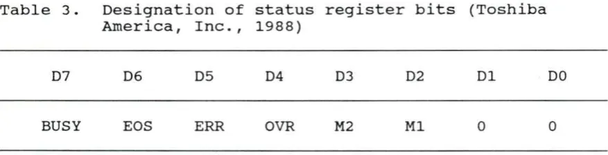
Status register The status register is an eight-bit
register that stores the status of the T6668. The status is read under CPU control by setting pins CE and RD low causing the status data to be output on pins DO to D7. The
MICROPHONE
O.luF ~
rs
l
l uF+ SPEAKER
VDD(+5Vdc) CPUM :z: ... N E- H :z: 0
E-H u u :::::> 0 H < :::::>
u 0 < ....: 0 0
H u H ....: A0- A8 :;::: H t.I... H
::;: t.I...
Dout
PHRASE 4 DO-D3
SELECTION
-//,,
Din___J__ A0-A8
START D4
_J_
STOP D5 Din
Dout 2
BIT RATE D6,D7
J,,
WriteT 6 6 6 8 RECORDING/
RAS
REPRODUCING WR
SPEAK/ CE CASl
NO SOUND
--'--J;L;u;
ACL CAS2RESET
CAS3
RD CAS4
2 Ml ,M2 RAS
VDD or [ 256K ~
....
"""
Q) WEVSS l (GND) c ::l Q) 1-.
.,...; 0 1-. rJJ
>< >< > u
655 KHz
D
IOOpFl IOOpFl
l
O.luF
Figure 10. The T6668 wired for the manual mode (Toshiba America, Inc . , 1988)
[image:25.566.55.506.113.638.2]E-MICROPHONE
Ki
VDD( +5Vdc)
1
O.luF ~
+
+
:z: N E- H :Z: 0 r H UU :=>CIH<::=> U O<:...JCIO H U H ...J
L ~ U... ~ A0-A8 :.;;:: 0:: <:
I
Dout
- - - Ci
CPlJM
DO-D7
c
pu
.__ ____ ,.. CE~----..i RD
.__ ____ ,.. WR
._.. ____ ,.. ACL
VDD or
r--
2t--~
Ml , M2VSSl(GND) 256K c:
'M
><
lOOpF
l
T 6 6 6 8
655 KHz
D
;..) :i 0 >< A0-A8 Din Dout Write CASl ~--+---+----' CAS2 1---4---+----• CASJ ---4---+----• CAS4 ---~---~ c E-:.;;:: <: 0:: I :::: z <: 0:: I Ci l:l z: H z:i-.:.:.RA~S"'-_.._---• ~ :.;;::
WE ~
0
r.
lOOpFl
1
0.luF [image:26.569.50.503.110.635.2]when an undefined command is given to the T6668. The NOP command resets the ERR bit. The M2 and Ml bits have the same values as pins M2 and Ml of the T6668, and their values are based on the number of D-RAMS used. The last two status
register bits corresponding to pins Dl and DO do not indicate status and are always set low.
Table 3. Designation of status register bits (Toshiba America, Inc., 1988)
D7 D6 D5 D4 D3 D2 Dl
BUSY EOS ERR OVR M2 Ml 0
Audio circuit
DO
0
The output of the bandpass filter (FILOUT) is connected to the input of an audio amplification circuit before being sent to the speaker during voice reproduction. The audio circuit and its connections to the T6668 are shown in Figure 12.
The LM386 is a low-voltage audio amplifier that provides a gain of 200 when pins 1 and 8 are connected by a capacitor. The positive input (pin 3) is connected to a 20K potentiometer to control the volume. The DVM-1 does not include a speaker, but does provide a 3.5 mm jack for an external speaker
[image:27.566.51.490.251.363.2]Power circuit
Power to the DVM-1 is applied to a jack which accepts a 5 .5mm X 2.0mm plug. The power requirement is 9-18 volts DC for the audio circuit; however, a transistor circuit is used to reduce this voltage to 5 volts DC for powering the T6668 and D-RAM. The location of the power jac k is shown in Figure
1.
9-18Vdc
27K O.OluF l OuF
DAO I
l..
8 OHMSPEAKER
FI LIN l OuF
2
FILO UT 220uF
5
TS2 +
TSl 3
+ 10
MICIN
1
22uFT6668 _L 0 . 05uF
Figure 12. The audio circuit and its connection to the T6668
Memory
[image:28.569.39.507.109.615.2]Pins AO to AB address 262,144 memory locations. Pins AO to A7 specify 256 rows or columns, and pin AB specifies one of two sets of 256 rows or c olumns (Texas Instruments, Inc.,
19B4). The row-address strobe (RAS) latches bits AO to AB as the row address, and the column-address strobe (CAS) latches
AO to AB as the column address.
PIN NOMENCLATURE
A8 1 16
vss
A0-A8 Address InputsD 2 15 CAS CAS Column Address Strobe
w
3 14 Q D Data-inRAS 4 13 A6 Q Data- out
AO 5 12 A3 RAS Row Address Strobe
A2 6 11 A4
w
Write EnableAl 7 10 AS VDD +5-V Supply
VDD 8 9 A7
vss
GroundFigure 13. Pin diagram and nomenclature for a 256 Kbit D-RAM (Texas Instruments, Inc . , 19B4)
The write enable (W) input selects the read or write mode. The read mode is selected when the write enable input
is set high, and the write mode is selected when the input is low .
The data-in pin (D) receives data during a write
operation, and data exit the data-out pin (Q) during a read
operation.
The 256 Kbit D-RAM must be refreshed at least once every four milliseconds by strobing each of the 256 rows specified by bits AO to A7 (Texas Instruments, Inc., 1984).
Control switches
Since the DVM-1 uses the T6668 in manual mode, switches are needed to control the device. The switches are shown in Figure 1; they include an a-position SPST DIP switch and three momentary contact push-button switches.
DIP switch switches 1 and 2 (labeled BitO and Bitl,
respectively) are used to select the recording bit rate according to Table 4. Switches 3, 4, 5, and 6 (labeled PH3, PH2, PHl, and PHO, respectively) are used to designate one of sixteen independent phrase recordings, as shown in Table 5. Switches 7 and 8 (labeled Ml and M2, respectively) indicate the number of D-RAMs installed, as indicated in Table 6.
Table 4. Selection of recording bit rate using switches 1 and 2
Recording Bit Rate Switch 1 Switch 2
8 Kbits/sec OFF OFF
11 Kbits/sec ON ON
16 Kbits/sec OFF ON
32 Kbits/sec ON ON
Push-button switches The push-button switches are
[image:30.566.88.506.500.626.2]Table 5. Designation of phrase number using switches 3, 4, 5, and 6
Phrase Number Switch 3 switch 4 switch 5 Switch 6
0 OFF OFF OFF OFF
1 OFF OFF OFF ON
2 OFF OFF ON OFF
3 OFF OFF ON ON
4 OFF ON OFF OFF
5 OFF ON OFF ON
6 OFF ON ON OFF
7 OFF ON ON ON
8 ON OFF OFF OFF
9 ON OFF OFF ON
10 ON OFF ON OFF
11 ON OFF ON ON
12 ON ON OFF OFF
13 ON ON OFF ON
14 ON ON ON OFF
15 ON ON ON ON
Table 6. Indication of the number of D-RAMs installed
based on switch 7 and 8 settings
Number of D-RAMs Installed
1
2 3 4
Switch 7
OFF OFF ON ON
Switch 8
OFF ON OFF ON
to reset the address counter allowing a new recording to be made in place of a previous recording. Depressing the record switch starts the recording process, and releasing the switch stops recording. Momentarily depressing the play switch
[image:31.566.49.511.106.374.2]The MC-lZ Single-Board Computer
The MC-lZ by Basicon, Inc. is a single-board computer intended for real-time process control applications. The MC-lZ is inexpensive, compact, and easy to use. The main components of the MC-lZ include:
1. The Zilog Z8671 microcomputer
2. The Intel 8255A programmable peripheral interface (PPI)
3. The National Semiconductor MM58274 programmable real-time clock/calendar
4. A 2K by 8 or an SK by 8 CMOS RAM
5. An application socket for an EPROM or RAM expansion 6. The RS232 serial interface buffer
7. A power supply module
8. A negative voltage generator
A block diagram of the MC-lZ is given in Figure 14, and a memory map is shown in Figure 15.
The Zilog Z8671 microcomputer
The Z8671 is an eight-bit microcomputer preprogrammed with a BASIC/DEBUG interpreter capable of accessing the
internal registers and external memory (Zilog, Inc., 1984). In addition to 2K bytes of on-chip ROM for storing the
BASIC/DEBUG interpreter, the Z8671 also has a 144-byte
register file, an on-board UART, two counter/timers, and 32
I/O lines provided by ports
o,
1, 2, and 3. A block diagramNEGATIVE VOLTAGE GENERATOR
POWER SUPPLY MODULE
---BATTERY
2K / 8K RAM
CLOCK / CALENDAR
RS232
BUFFER CRT
l
PORTS~
14 I / Ol-
~-~~--~---Z8671
8255A PPI
APPLICATION SOCKET
RESET CIRCUIT
24 I / 0
[image:33.569.50.500.98.659.2]HEXADECIMAL SIZE
ADDRESS (BYTES)
FFFD
I
BAUD RATE SELECT 1B803
I
8255A PPI 4B800
A80F
I
CLOCK /CALENDAR 16A800
4FFF Z8 VARIABLES (l / 4K)
---
-
- -
-
---·
RAM 8K
3000
lFFF
EPROM (EXPANDABLE TO 8K)
4K r- AUTO-START AT 1020
1000
07FF
[image:34.567.65.472.98.635.2]0000 Z8 BASIC AND REGISTERS 2K
OUTPUT INPUT Vee GND XTAL As Os RJW RESET
1111
! !
l
l
MACHINE TIMING & IN STRUCTION CONTROL
UART ALU
PROGRAM
FLAGS MEMORY
TIMER! 2048 • 8·BIT
COUNTERS (2)
REG. POINTER
REGISTER FILE PROGRAM
INTERRUPT 124 x 8·BIT COUNTER
CONTROL
PORT 2 PORT 0 PORT 1
11111111
1/0 ADDRESS OR 1/0E
ADDRESS/DATA OR 1/0B
(BIT PROGRAMMABLE) (NIBBLE PROGRAMMABLE) (BYTE PROGRAMMABLE)
Figure 16. Block diagram of the Z8671 (Zilog, Inc., 1984)
BASIC/DEBUG interpreter The BASIC/DEBUG interpreter
recognizes a form of Dartmouth BASIC called BASIC/ DEBUG. Since BASIC/ DEBUG is i ntended for process control applica-t ions, Darapplica-tmouapplica-th BASIC capabiliapplica-ties such as applica-trigonome applica-tric functions, arrays, and fractional numbers have been excluded
[image:35.563.96.444.85.398.2]Variables The 26 available variables are represented by each letter of the alphabet. Each variable occupies two bytes of RAM for storing numerical values (Zilog, Inc., 1981).
Operators Operators signify a calculation that
may be arithmetic or relational. The arithmetic operators
include addition (+), subtraction(-), multiplication (*), and
division (/). The relational operators are listed in Table 7 .
Table 7. Relational operators supported by BASIC/ DEBUG (Zilog, Inc., 1981)
SYMBOL MEANING
= equal
<= less than or equal
< less than
<> not equal
> greater than
>= greater than or equal
Functions The two functions are AND, for
performing logical AND, and USR, for accessing machine language subroutines (Zilog, Inc., 1981).
Commands The commands are listed and briefly
explained in Table 8.
Ports 2 and 3 Port 2 provides 8 I/O lines that can be
Table 8. Commands recognized by BASIC/ DEBUG
COMMAND
GO@
GO SUB
GOTO IF/ THEN INPUT, IN
LET
LIST NEW
PRINT, PRINTHEX
REM RETURN
RUN STOP
FUNCTION
Unconditional branching to a machine language subroutine
Unconditional branching to a BASIC subroutine
Unconditional branching within a program Conditional branching and operations Data entry
Value assignme nt to a variable or memory location
Displays memory on the CRT s c reen Clears memory for a new program
Displays characters and/ or numerical values on the CRT screen
Signifies a program remark
Indicates the end of a BASIC subrouti n e Starts program execution
Ends program execution
shown in Figure 17, a Port 2 mode register bit set high
designates the corresponding Port 2 bit as an input, and a b i t set low produces an output line. By equating address 246
(@246) to a decimal value between O and 255 or a hexadecimal
[image:37.558.50.507.72.524.2]@246=%00 or 0 07-00 are output lines
@246=%0F or 15 07-04 are output lines
03-00 are input lines
@246=%FO or 240 07-04 are input lines
03-00 are output lines
@246=%FF or 255 07-DO are input lines
07 06 05 04 03 02 Dl DO
x
x
x
x
x
x
x
x
Note : X=O , output . X=l , input.
Figure 17. The Port 2 mode register (Zilog, Inc., 1984)
Port 3 provides 4 input lines {D0-03) and 4 output lines (D4-D7). In addition to the I/O function, Port 3 lines can be configured for handshake I/O, interrupt requests, serial I / O, and counting/timing. The various functions are selected by writing a control word to the Port 3 mode register located at address 247 (@247). For example, if @247=%41 then Port 3 is set for input on lines D0-03 and output on lines 04-07. In the MC-lZ system, lines DO and 07 are used for serial
communication with a terminal leaving 6 lines {Dl-06) of Port 3 directly available to the user.
The 8255A programmable peripheral interface (PPI)
The Intel 8255A PPI provides 24 input/output lines that
[image:38.564.50.488.84.606.2]PPI also has a control register to program the ports for input or output. The high and low nibbles of port C can be
programmed independently.
In the MC-lZ system, the 8255A PPI is located in four successive memory addresses:
%B800 Port A
%B801 Port B
%B802 Port C
%B803 PPI control register
Ports A, B, and C are set for input or output by writing to the control register at location %B803. The control register is shown in Figure 18, and the possible input/ output
combinations for the ports are listed in Table 9.
D7 D6 DS D4 D3 D2 Dl DO
1 0 0
x
x
0x
x
Note : X=O, out put . X=l , in put.
Figure 18. The control register for setting ports A, B, and
c
for input and/ or output (Uffenbeck, 1985)
[image:39.566.55.503.79.726.2]Table 9. Possible I/O combinations for ports A, B, and C (Basicon, Inc., 1984)
Hexadecimal Port C Port
c
Value of Port A Port B High Low
@%B803 Nibble Nibble
%80 OUTPUT OUTPUT OUTPUT OUTPUT
%81 OUTPUT OUTPUT OUTPUT INPUT
%82 OUTPUT INPUT OUTPUT OUTPUT
%83 OUTPUT INPUT OUTPUT INPUT
%88 OUTPUT OUTPUT INPUT OUTPUT
%89 OUTPUT OUTPUT INPUT INPUT
%8A OUTPUT INPUT INPUT OUTPUT
%8B OUTPUT INPUT INPUT INPUT
%90 INPUT OUTPUT OUTPUT OUTPUT
%91 INPUT OUTPUT OUTPUT INPUT
%92 INPUT INPUT OUTPUT OUTPUT
%93 INPUT INPUT OUTPUT INPUT
%98 INPUT OUTPUT INPUT OUTPUT
%99 INPUT OUTPUT INPUT INPUT
%9A INPUT INPUT INPUT OUTPUT
%9B INPUT INPUT INPUT INPUT
The MM58274 clock/calendar
The National Semiconductor MM58274 provides a program-mable, real-time clock/calendar for the MC-lZ system. The clock measures tenths of seconds through years and also accounts for leap years (Basicon, Inc., 1984) . The
clock/calendar counters are four-bit counters that use bits DO-D3 of the data bus. The various counters and their
respective memory addresses and modes are listed in Table 10.
2K/8K RAM socket
[image:40.567.54.505.88.396.2]reserved for RAM, the MC-lZ is ready to operate with an SK RAM provided jumper E4 is installed (Basicon, Inc., 1984). To use a 2K RAM, jumper E5 must be installed, and a short sequence of data must be written to the ZS registers to allow the MC-lZ to adjust to the change in memory (Basicon, Inc., 1984). The MC-lZ system used in this project has 8K bytes of RAM for storing programs; however, the top l/4K bytes are designated for
BASIC/DEBUG variables and other functions (Basicon, Inc., 1984) .
Table 10. Clock counters and their addresses and modes (Basicon, Inc., 1984)
Address Counter Mode
%A800 Control register Split read and
%A801 Tenths of seconds Read only
%A802 Units of seconds Read or write
%A803 Tens of seconds Read or write
%A804 Units of minutes Read or write
%A805 Tens of minutes Read or write
%A806 Units of hours Read or write
%A807 Tens of hours Read or write
%A808 Units of hours Read or write
%A809 Tens of hours Read or write
%A80A Units of months Read or write
%A80B Tens of months Read or write
%A80C Units of years Read or write
%A80D Tens of years Read or write
%A80E Day of week Read or write
%A80F Clock setting/ Read or write
interrupt reg.
The MC-lZ application socket
The application socket accepts a 4K/ 8K EPROM or a 2K/8K RAM (Basicon, Inc., 1984). The memory allocated for the application socket exists between addresses %1000 and %2FFF, but since this MC-lZ system uses a 4K EPROM, only memory between %1000 and %1FFF is used. One feature of the Z8671 allows a program to automatically start when the system is powered. For this feature to work, the program must start at address %1020 and contain a line number between O and 255
followed by
a
BASIC program statement (Basicon, Inc., 1984).The RS-232C serial interface buffer
To standardize connections between terminals and modems, the RS-232C standard was developed in the early 1960s to
define logic levels, maximum baud rates (bits/second), maximum cable lengths, and connector types (Uffenbeck, 1985). The RS-232C standard has a maximum baud rate of 20K for a 50 foot cable. The RS-232C standard defines a voltage between +3 and +25 as logic
o
and a voltage between -3 and -25 as logic 1. These logic levels provide a minimum of 2 V of noise immunity which is necessary for dealing with the capacitive and DCport 3 of the Z8671 microcomputer. The transmitter converts the serial output signal from port 3 (07) into an RS-232C compatible signal that is sent to the CRT terminal. A ground wire completes the 3-wire serial communication system of the
MC-lZ.
Power supply module
The MC-lZ requires a +5 Vdc (+/ - 5%) power source that can deliver 250 mA or 500 mA when the EPROM programmer is used. The power supply module provides +5 Vdc to the Z8671 microcomputer and the negative voltage generator discussed in the next section. The power supply module also has a 100 mA-hr., 3.6 volt nickel-cadmium battery to maintain programs stored in RAM and to keep the calendar/ clock running when power is interrupted (Basicon, Inc., 1984). The battery is trickle-charged through a charging resistor included with the MC-lZ. The power supply module also contains a DB25S
connector allowing connection to any standard RS-232 cable, a push-button switch for resetting the system without disturbing the RAM contents, a power ON-OFF switch, and an LED power
indicator .
Negative voltage generator
Interfacing the DVM-1 to the MC-lZ
Interfacing the digital voice recorder (DVM-1) to the single- board computer (MC-lZ} involves alterations to the DVM-1 board and development of an interface circuit.
DVM-1 alterations
Alterations to the DVM-1 are necessary to make the control pins of the T6668 (RD, WR, CE, ACL, CPUM, AND DO-D7) available for direct connection to the ribbon cable from the interface circuit. Pins DO, Dl, 02, 03, 06, and D7 are
connected to the off side of the DIP switch. Wires soldered to this side can be used to access the pins provided the switches are off to insure electrical isolation from the original circuit.
Pins D4, D5, WR, and ACL are also connected to components on the DVM-1 board. These pins are electrically isolated by breaking the path between the pin and the components to which they were connected. Wires are then soldered on each side of the break allowing the circuit to be reconnected in its
original form.
1. Prepare the surfaces to be glued by cleaning them with ethanol.
2. Mix equal parts of the two-component conductive adhesive.
3. Dip the stripped end of a 30-gauge wire into the conductive adhesive mixture to coat the wire.
4. Lay this end of the wire onto the pin of the T6668. 5. Hold the wire in place with a wirewrap post clamped
into a hemostat. The notched end of the post sets on the wire, and the weight of the hemostat holds the wire down until the adhesive sets overnight.
6. The remaining length of the wire is secured to the DVM-1 board using drops of 5-minute epoxy.
Pin CE is handled in the same manner as pin CPUM. Since pin RD is not used in the manual mode, it is accessed by simply glueing a wire to the pin. All of the wires, as well as wires from +5 volts and ground, are soldered to a 2 X 13 pin header mounted to the DVM-1 board. The circuit alterations are shown schematically in Figure 19.
The interface circuit
The interface circuit consists of a ribbon cable for connection to the DVM-1 pin header, control switches for selecting manual or CPU control, and a 2 X 13 pin header for connection to the ribbon cable from the PPI register.
The control switches are SPDT toggle switches that allow the DVM-1 board to be operated in the manual mode as
originally intended or by CPU control. The switches are associated with pins D4, D5, WR, and ACL which are
the electri cal path between the T6668 and the c omponents. Wires soldered to the T6668 side o f the break are label ed 0 4,
;f-if
i{f
1
1i-r
.--=--=--=--=-ii
, -
~
-
- - , ' I I
I
r-, '
I I
I :
I I
e
I
I
2 X 13 PinI
I
I
I I I
I
I
HeaderI
I
I I I I
I I
I
I
I
1r-H--_J
IL.'.::+-+=:t.:t"++
+-==--,
11111
11
L--.r+--t_:t-++-t=--::11
I
I
~+-n---1---+
I I
11I I
1I
I
I I
L
L--,
I
I
I
J
I
I
I I
L _-:_
~
+
...!. ..i.-+
t- __
1
I
I
1I
I
I
---rTT...J
1 1111 1
11
1,
---+-t-+-J,
:' 1111
11 11
---+-t-J
'1'11
11 II
---+-+---J
+sv
11
,1
I
L.:..-t~-
I
L+ ·- - ---t-~--, - - - -I I 1 1
I I
I
L
- - -
11111
_J
I
I
I
r---1--1---+--+-~ ~---B~1.tl
I
I
I
I
RD WR NC CE NC D7 D6 DS D4 03
,--
_J1,
I
~...--
I I
_JI
I I
r-1'~-
_J
I
I
x
T6668 NC
D2
Dl
Break in circuit path
DO
Added wire
CPUM
- - Existing wire
•
Soldered connection ACL ~H1.____J
O Glued connection
PHO RESET PUSH-BUTTON DIP SWITCH
[image:46.564.52.508.164.650.2]05, WR, and ACL and are connected to the center post of the SPOT switch. The corresponding wires soldered on the other side of the break are labeled 04', 05', WR', and ACL' and are each connected to one of two remaining posts of the toggle switch. This arrangement allows the break in the electrical path to be bypassed returning the circuit to its original form.
The remaining post of each toggle switch is wired to a 2 X 13 pin header for connection to the PPI register. When the switches connect pins 04, 05, WR, and ACL to the pin
header, computer control is possible. Pin CPUM is also wired to a toggle switch with ground wired to one post and +5 Vdc wired to the other post. As shown in Figure 20, pins D0-07 are connected to port A (AO-A7), and pins ACL, WR, RD, and CE are connected to bits B3, B2, Bl, and BO, respectively.
Software
The software allows the MC-lZ to control the DVM-1 by writing commands to the T6668 microprocessor. A listing of the T6668 commands is given in Table 11. All of the commands require 8 bits (1 byte) except for the ADLDl and ADLD2
commands which require 24 bits (3 bytes) for addressing all of the bits in memory.
Bl, and BO of port B, respectively. To s i gnify that a command is going to be written, pins CE and WR must be set low. The
I
ISocket __..,
Connector
•
I
L L+SV
1,l. l
D4
-
CPUM---...J D4
I --..J"
-...J ....,,
GND - A3 A2
--
-
Al AO-DS
-..L
---...J"
DS'
....,, A4
AS A6 WR
-A7
~
WR '
...1
~ PPI
l Pin
ACL Header
~ ACL'
-
BO-
~ BlB2 B3 1
[image:48.564.46.501.143.671.2]Table 11. T6668 commands {Toshiba America, Inc., 1988)
command D7 D6 DS D4 D3 D2 Dl DO Function
NOP 0 0 0 0
x x x x
Selects the soundreproduction mode
START 0 0 0 1
x x x x
Starts recording/re-production in the Direct mode
STOP 0 0 1 0
x
x x
x
Stops soundrecord-ing/ reproduction in the Label/ Index mode
ADLDl 0 0 1 1 Al9 Al8 Al7 Al6 Specifies the start
AlS Al4 Al3 Al2 All AlO A9 A8 address in the
A7 A6 AS A4 A3 A2 Al AO Direct mode(3 bytes)
ADLD2 0 1 0 0 Al9 Al8 Al7 Al6 Specifies the end
AlS Al4 Al3 Al2 All AlO A9 A8 address in the
A7 A6 AS A4 A3 A2 Al AO Direct mode{3 bytes)
CNDT 0 1 0 1
x
SL BRl BRO SL selects sounds(O)or silent{l) mode. BRl and BRO specify bit rate(bits/ sec.)
LABEL 0 1 1 0 LB3 LB2 LBl LBO Starts recording/
reproduction in the Label/Index mode
ADRD 0 1 1 1
x
x x
x
Allows the addresscounter to be read
0 0 0 0 Al9 Al8 Al7 Al6 in 3 successive read
Al5 Al4 Al3 Al2 All AlO A9 A8 operations as shown
A7 A6 AS A4 A3 A2 Al AO to the left
REC 1 0 0 0
x x x x
Selects the soundrecording mode
[image:49.565.54.514.83.639.2]command is actually written after pins CE and WR are returned to their normal state of logic 1 (Toshiba America, Inc.,
1988) . The commands provide two different recording/
reproduction modes called the Label/ Index mode and Direct
mode.
Label/Index mode
As with manual control, the Label/ Index mode uses part of the memory as an index area for storing start and stop
addresses and is also capable of storing 16 different recordings . Recording is accomplished as follows:
1. Resetting the address counter of the T6668 by setting the ACL pin low and then high.
2. Inputting the REC command to set the T6668 in the recording mode .
3. Entering the CNDT command to spe cify the bit rate. 4. Inputting the LABEL command to indicate phrase
number.
Recording begins after the LABEL command is entered and stops when the STOP command is given. The corresponding port values and command statements for each step of the recording process are given in Table 12. A sample program is listed in Appendix B.
Reprodu ction in the Label/ Index mode is accomplished b y : 1. Entering the NOP command to set the T6668 into the
reproduction mode.
Reproduction begins after the LABEL command is entered and stops when the recording ends. The command sequence is:
@A=%00: @B=lO: @B=15 (writing the NOP command) @A=%68: @B=lO: @B=15 (writing the LABEL command)
Table 12. Function, port value, and command statement for each step of the recording process in the
Label/ Index mode
Function or Command
Reset the address counter
REC
*
CNDT ( 32K)
*
LABEL(#8)*
STOP
*
* .
Writescommand to the T6668
Port A or B Values 07---DO
x x x
X A
!'.!B
~0 0 0 0 0 1 1 1 0 0 0 0 1 1 1 1
1. .§. 2 ~ .1 2. .l Q 1 0 0 0 0 0 0 0 0 1 0 1 0 0 1 1
0 1 1 0 1 0 0 0 0 0 1 0 0 0 0 0
X X X X A
!'.!B
~0 0 0 0 1 0 1 0 0 0 0 0 1 1 1 1
Command Statement
@B=7 or @B=%07 @B=15 or @B=%0F
@A=128 or @A=%80 @A=83 or @A=%53 @A=104 or @A=%68 @A=32 or @A=%20
@B=lO or @B=%0A @B=l5 or @B=%0F
X = don't care
R
=
RD (Read) A = ACL (Reset) C = CE (Chip Enable) W = WR (Write) % indicates a hexadecimal numberDirect mode
In the Direct mode, the ADLDl and ADLD2 commands specify the memory start and stop addresses, respectively. The Direct mode has two advantages compared to the Label/Index mode:
1. Since the start and stop addresses are specified by commands, an index area is not needed allowing more memory space for voice storage.
2. By designating start and stop addresses, an
indefinite number of phrases can be independently recorded compared to the maximum of 16 phrases allowed in the Label/ Index mode.
The recording process is started by following these steps: 1. Setting the ACL pin low and then high to reset the
address counter
2. Inputting the REC command to set the T6668 into the recording mode.
3. Inputting the CNDT command to specify the bit rate. 4. Entering the ADLDl and ADLD2 commands to designate
the start and stop addresses, respectively.
5. Inputting the START command to begin voice recording. Recording stops when the stop address is reached. The command sequence is similar to the previous example except that
commands ADLDl and ADLD2 each require three write sequences since they each occupy three bytes. The high nibble of the first byte indicates whether the address is a start or stop address. The remaining 2 and 1/2 bytes (20 bits) are used to
address the memory. A sample program is given in Appendix
c.
1. Inputting the NOP command to set the T6668 into the reproduction mode.
2. Entering the ADLDl and ADLD2 commands to specify the region of memory to be reproduced.
3. Inputting the START command to begin voice reproduction.
Reproduction stops at the stop address.
Firmware
The firmware is a utility PROM (ZUTIL-1.00) that supports the MC-lZ by offering 14 commands for program development . The PROM consists of a main program written in BASIC and several machine code subroutines for fast execution of
commands. With the PROM installed in the MC-lZ application socket, the utility program automatically starts running when the MC-lZ system is powered or reset. The utility program is stopped by pressing the ESCape key and then the RETURN key. The 14 available commands and their functions are listed in Table 13.
Two situations for using these commands include preparing the RAM before entering a BASIC program and transferring a program in RAM to an EPROM. To prepare the RAM, the F command fills the RAM with %FF, and the M command marks the beginning of the program . To transfer the program to an EPROM, the D command is first used to determine the RAM address where the program ends. This address is needed when specifying what part of the RAM gets copied to the EPROM. The E command
is then entered to start the copying process. The V command verifies whether or not the copying was successful. The R command displays the contents of the EPROM to see what was copied. Most of these utility commands include an argument consisting of a starting, ending, and/ or destination address.
Table 13. Commands offered by the MC-lZ utility PROM
Command
A (Alter memory)
c
(Copy memory)D (Display memory) F (Fill memory)
E (Erase check)
p (Program EPROM)
v
(Verify EPROM)R (ROM display) M (Mark top)
L (Locate)
H (Help)
s
(Set time) T (Time check)Function
Allows direct access to memory for changing bytes
Copies any section of memory to another area of memory
Displays the RAM contents
Fills any memory location with a chosen hexadecimal value
Checks EPROM bytes to see if they equal %FF
Copies RAM contents into EPROM Verifies whether or not EPROM contents match the RAM contents Displays contents of EPROM
Marks the beginning of a program Searches memory for a selected hexadecimal number
Displays a list of utility commands Sets the clock/calendar
[image:54.567.60.508.210.684.2]SPEECH RECOGNITION
Literature Review
Speech recognition is the process of differentiating words in a vocabulary spoken by the same person or different people. The following discussion of speech recognition
includes the problems of accomplishing speech recognition, the categories of speech recognition, the speech recognition
process, and applications of speech recognition for the disabled.
Problems
The problems of speech recognition include ambiguities of speech and variations in pronunciation between different
speakers or from the same speaker.
Ambiguities of speech One of the ambiguities of
speech results from the pronunciation of words in continuous speech. Continuous speech is the pronunciation of words
without pauses between the words in which the individual words can still be discerned by the individual (Wallich, 1987 ). The ambiguity arises when the pronunciation of a group of adjacent words suggests more than one possible combination of words. For example, a speech recognizer would have difficulty
One way to avoid the ambiguities of continuous speech is to "isolate" words during speech. Isolated words are words spoken with a long enough pause between them so that the pronunciation of a word is not affected by words immediately before or after it (Wallich, 1987). Unfortunately, this style of speech also has ambiguities due to words with the same
pronunciation called homonyms. Examples of homonyms include "great" and "grate," and "to," "two," and "too."
Variations in pronunciation Dialects are one cause of
variations in pronunciation between different speakers. For example, one person might pronounce the word "creek" as
"creek" while another person would pronounce it as "crick." Accents are another source of variations in pronunciation.
Variations in pronunciation also occur with the same
person. A person may change word pronunciation as a result of speaking faster. For example, "bread and butter" can be
spoken faster by saying "bread 'n' butter," or even faster by saying "brembutter" (Hollingum and Cassford, 1988). Other factors affecting pronunciation include emotional status or a physical condition such as a cold.
Categories
1 . Isolated-word/ speaker-dependent 2. Isolated-word/ speaker-independent 3. Continuous-speech/ speaker-dependent 4. Continuous-speech/ speaker- independent
The first category is the least sophisticated because it only considers isolated words and speech from one person (speaker-dependent). The second category is more difficult because it includes speech input from any person (speaker-independent) . The next two categories have increased capability because they allow continuous speech; however, the fourth category is mor e sophisticated because it accepts speech from anyone. Eac h o f these categories can be further classified based on the number of words that can be recognized.
The speech recognition process
The speech recognition process begins with the production of speech -sound from the human vocal tract . The speech sound is collected by a microphone for conversion into an electrical signal. Various speech signal acquisition and analysis
techniques extract the necessary information used by the speech recognition algorithms to differentiate words.
Speech sound production The sounds of speech are
vibration which contributes to voice pitch. The speech sound is then altered as it passes through the throat (pharynx), oral, and nasal cavities. These cavi ties act as resonators t o produce various tones much like the pipes of a pipe organ
(Cater, 1984). In addition to the vocal chords and resonant
Nasal cavity
Pluirynx
Vocal -~r--+-~
cords
Trachea
[image:58.565.82.462.84.659.2]cavities, the tongue, palate, teeth, and lips also affect the speech sound to enable the pronunciation of all the basic
sounds of a language. These basic sounds are called phonemes. The phonemes are distinguishable by the resonances
produced by the cavities. Each of the three cavities produces a unique resonant frequency for a particular sound. This
frequency is called a formant frequency which is evident in the speech spectrum shown in Figure 22. The first, second, and third formants are associated with the throat, nasal, and oral cavities, respectively (Cater, 1984). Although other formants may be present, they do not contribute significantly to the total energy of the speech spectrum. Depending on the
50
SECOND FORMANT
1r21 40
;;;
E
...
C>~ 30
:::;
...
:IE c
20
0 2
FREQUENCY (kHz)
[image:59.566.130.422.398.647.2]phoneme spoken, each formant will reside in a particular frequency band as indicated in Table 14 which lists the formant resonances of the vowel sounds.
Table 14. Formant resonances of vowel sounds (Cater, 1984)
Fl F2 F3
Vowel Resonance(Hz) Resonance(Hz) Resonance(Hz)
ee(eat) 210-330 2230-2350 2950-3070
i(bit) 330-450 1930-2050 2490-2610
eh(bet) 470-590 1780-1900 2420-2540
ae(bat) 600-720 1660-1780 2350-2470
ah(top) 670-790 1030-1150 2380-2500
aw(ball) 510-630 780-900 2350-2470
oo(book) 380-500 960-1080 2180-2300
oo(moon) 240-360 810-930 2180- 2300
uh(tug) 580-700 1130-1250 2330- 2450
er(nerve) 430-550 1290-1410 1630-1750
Speech signal acquisition The purpose of speech
signal acquisition is to convert the acoustic speech signal, collected by the microphone, into a form that will allow
features to be extracted. These features enable sounds to be characterized for the purpose of speech recognition. Two primary methods of speech signal acquisition are direct
wave-form acquisition and spectral signal acquisition (Cater, 1984) •
Direct waveform acquisition Direct waveform
acquisition is the result of digitizing the analog speech
an analog-to-digital converter can convert the signal into a voltage-equivalent binary data byte (Cater, 1984).
Delta modulation encoding is another method of directly digitizing the speech signal. Instead of representing each sample with its own data byte as in waveform encoding, delta modulation encoding only records the changes in the speech signal without concern for the actual voltage of the sample.
Spectral signal acquisition Spectral signal
acquisition obtains the speech frequencies directly from the speech signal by filtering the signal before performing any digitization. This method uses several bandpass filters that span the frequency range of the speech signal. The filters extract the various frequency components which are then digitized and stored in separate registers of the computer
(Cater, 1984). The filtering can be analog, digital, or mathematical.
Speech signal analysis Speech signal analysis
extracts features from the information provided by speech signal acquisition. The main methods of feature extraction include the zero-crossing technique, Fast-Fourier Transform
(FFT), and linear predictive coding (LPC).
Zero-crossing technique This technique filters
set period of time. The counting is a measure of the extent of each formant in a particular sound. The counter values are the extracted features used in speech recognition.
Fast-Fourier Transform CFFT) FFT is a
mathematical process that converts a time-varying signal
directly into a signal spectrum representing the energy of the signal as a function of frequency. The process is illustrated in Figure 23. A sequence of FFTs forms a spectrogram as shown in Figure 24. The spectrogram acts as a "fingerprint" for distinguishing sounds in speech recognition.
Figure 23.
1
/.m
-1 w t--;-;;- . .., s( t)e dt
rl
2Frequency
Inpu t signal
Fourier transform
Signal spectrum
°' /
l
'\.
Signal-gr
components{
~~ 1210:\
E
<(
Time
[image:62.565.190.357.365.652.2]