Abstract: CMOS technology plays an important role in the modern electronics world. CMOS technology also plays significant role in aerospace applications. To store data, memories are widely used as the medium in aerospace applications. SRAM cells are the memories made by the CMOS technology. The most vital issues faced by memories are due to single event upsets (SEUs) which are induced by radiation particles. The SEU’s due to increase in densities and SEU’s. There is a decrease in critical charge and supply voltage in CMOS process technology. There is a need for a technique which can to tolerate these SEU’s in such aerospace applications. Which are in the environment of complex celestial radiation? The technique which is considered for such environment is radiation-hardened by design (RHBD) with soft error robustness. This paper aims at is proposing an area efficient and high reliable RHBD memory cell for the above said application using 45nm technology in Cadence Tool. Depending on power, write/read time, the layout area of 14T, 12T and 10T RHBD memory cells and their performance on power for read/write operations are observed. A comparative study is also done on these memory cells based the parameters considered.
Keywords: Architecture, CMOS, RHBD. I. INTRODUCTION
Memories represent the important part in modern circuit designs .SRAM plays a key role in electronic systems that are widely used as memories. SRAMs were designed using reduced delay, area, power and reliability calculation in [1].In general, SRAM cells are highly affected to reliability changes due to high densities, low critical charge and low supply voltage .In SRAM cells a particle impact can change the state of cells leading to formation of single event upset. The active particles help SRAMs in challenging with the reliability triggering. The electronic device faces the malfunctioning by a failure mechanism known as single event upsets (SEUs) by changing the pre-stored charge temporarily [2]. The transient voltage pulse is generated. When the stored value in a node was modified. By using move-coupled inverters, the 6T SRAM cell is usually built. The charge which is generated in the stored node can trigger observations mechanism, in order to turn the domain in any other responsive node when an error takes place in the memory, due to which data overwrites happens and faults occurs [3-4]. In general with CMOS technique, SRAM cells will be further liable to this reliability task due to increasing densities, reducing critical charge, and
Revised Manuscript Received on August 05, 2019
M. Chaitanya, PG Scholar, GMR Institute of Technology, India
V. Kannan, Professor, Department of ECE, GMRIT, Rajam, India
lowering supply voltage [1]. Radiation-hardened by-design (RHBD) techniques plays major role in aerospace programs and these are designed in such a way that they can suit the aerospace environment [5-6]. The conventional SEU memory designs like 10T memory cell can tolerate single event upsets at a time but they can’t be good at multiple upsets at the same time [7]. To overcome multiple event upsets 12T memory cell was proposed and are effectively work in high radiation environments but consumes more power [8]. The radiation hardened 14T cell increases resilience to both single and multiple event upsets, due to the charge distribution among OFF-transistors. 14T memory cell optimizes speed and power over 12T memory cell [9].This paper is divided into the five sections. Section I is introduction, Section II explains about the different RHBD memory cell schematics with operation. In Section III, the 4×4 architecture of 10T RHBD memory cell and the performance analysis for various memory cells with write/read timings are shown. In Section IV results and discussions are done. Finally, a conclusion is presented in Section V.
II. SCHEMATICANDOPERATIONANALYSIS
A. 10T RHBD Memory:
10T RHBD memory cell offers the best reliability and can also be used for error recovery at particular sensitive node. It provides improved write and read access time. The schematic of 10T RHBD memory cell is shown in Figure 1.
Design And Analysis Of RHBD Memory Cells
And 4x4 RHBD 10T Memory Cell Architecture
Design And Analysis Of RHBD Memory Cells And 4x4 RHBD 10T Memory Cell Architecture
Figure 1: Schematic of RHBD 10T memory cell B. 12T RHBD Memory:
12T RHBD memory cell gives higher stability and tolerates both single node and multiple nodes upsets. It calculation for area, power and read/write access time has been done. The schematic of 12T RHBD memory cell is shown in Figure 2.
Figure 2: Schematic of 12T memory cell C. 14T RHBD Memory:
[image:2.595.304.560.50.250.2]The 14T RHBD memory cell utilizes isolation technique to achieve optimized speed and power. The schematic of 14T RHBD memory cell is shown in Figure 3.
Figure 3: Schematic of RHBD 14T memory cell
III. ARCHITECTURE
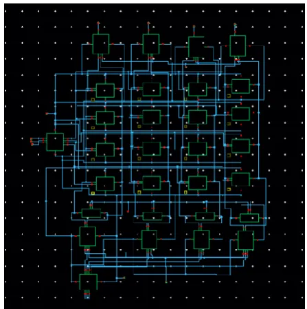
A 4×4 RHBD memory is designed by using i.e.2 to 4 decoders (both row and column decoders), sense amplifier circuit and write driver circuits. The main objective of the memory design is to perform the operation of read/write the data with reduced power and delay. The 2byte architecture schematic of RHBD memory cell is shown Figure 4.
Figure 4: Schematic of RHBD Memory cell architecture A. The Pre-Charge Circuit:
[image:2.595.54.284.390.628.2] [image:2.595.314.538.393.618.2]Figure 5: Schematic of Pre-charge circuit B. Row Decoder:
The block diagram for the N: 2N decoder and its connected circuitry are mentioned in the above diagram. Essentially, the decoder selects only one among 2N outputs, as according to the deal with input lines. The decoder output is given to the rows of SRAM cells, in according to the given N- bit address. Row decoder selects one of the memory rows and can be designed with the help of common logic gates.
C. Column Decoder:
For analyzing the data or to regulate its contents, the column decoder chooses a specific column inside the memory array of the chosen cell. Similar to the row decoder, the column selector is also choosing a particular column.
D. Write-Driver Circuit:
[image:3.595.46.266.50.354.2]The write-driver circuit discharges one of the bit lines i.e., bit line bar or bit line from the pre-charge circuit value which is in the write noise margin of the SRAM memory design. Usually, the write driver circuit is operated with Write Enable (WE) signal of the design to discharge and drives the bit line to ground from the precharge level. Write-driver circuit is designed by using two pass transistors and AND gates. The schematic of write-driver circuit is shown in Figure 6.
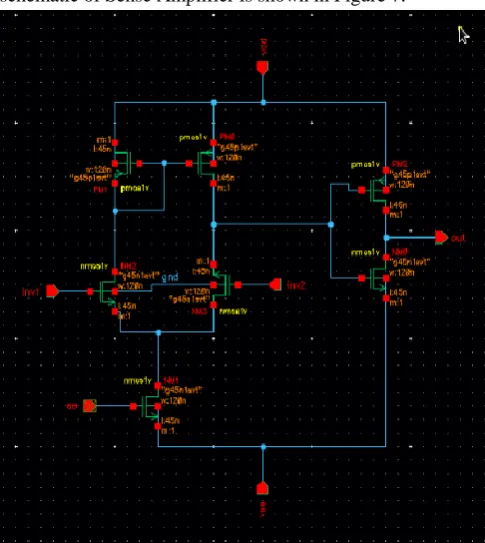
Figure 6: Schematic of write-driver circuit E. Sense Amplifier:
Sense amplifier (SA) circuit in SRAM memory architecture is used to perform bit line sense operation. Differential voltage is generated by the precharge circuit at the bit lines by significantly reducing the operational time. The principle of the sense amplifiers on each pair of bit lines is to turn the weak signal into a normal logic signal that can then be fed to additional data multiplexers and/or I/O pin drivers. The schematic of Sense Amplifier is shown in Figure 7.
[image:3.595.305.548.418.690.2]Design And Analysis Of RHBD Memory Cells And 4x4 RHBD 10T Memory Cell Architecture
IV. RESULTANDDISCUSSION
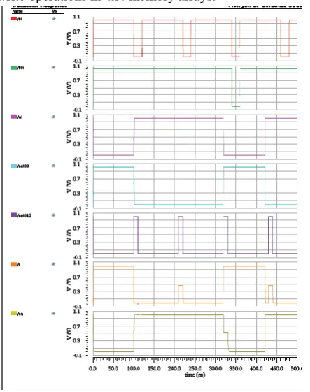
This Section presents the simulation results of 4x4 memory architecture, 10T RHBD memory, 12T RHBD memory, and 14T RHBD memory. Cadence virtuoso tool is used to simulate all the mentioned designs with the 45nm technology libraries. Figure 8 shows the transient response for read and write operations in 4x4 memory arrays.
[image:4.595.323.525.72.339.2]Figure 8: Simulation results of 10T RHBD Memory Figure 9 shows the 12T RHBD memories cell. It also shows the write 0, write 1, read 0, and read 1 operation and its simulation results.
Figure 9: Simulation results of 12T RHBD Memory Figure 10 shows 14T RHBD memory cell. It also shows the write 0, write 1, read 0 and read 1 operation and its simulation
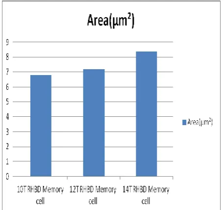
result. The parameter values obtained for different memory cells are shown in table 1.
Figure 10: Simulation results of 14T RHBD Memory. PARAMETERS COMPARISONS:
[image:4.595.49.271.145.426.2]The table 1 shows the values of the different memory cell parameters.
Table 1: Different memory cells parameter values
PARAMETERS
10T RHBD memory
12T RHBD memory
14T RHBD memory AREA(µm²)
6.89 7.12 8.26
POWER(nW) 20 38.9 55.6
DELAY(µs) 2 4.12 6.24
The parameters considered for the analysis are discussed below.
A. AREA:
[image:4.595.55.282.490.736.2]Figure 11: Area results of different RHBD Memory cells B. POWER:
[image:5.595.55.284.50.264.2]The power dissipation in different memory cells are shown in figure 12. The RHBD 10T memory cell exhibits low power dissipation than other hardened memory cells. The dissipation of power in the 10T memory cell is low is due to the usage of less PMOS transistors when compared with 12T and 14T cells. The power for the memory designs are also compared and shown in Figure 12.
Figure 12: Power results of different RHBD Memory cells
C. DELAY:
[image:5.595.53.285.392.586.2]The delay occurred in different memory cells are shown in Figure 13. RHBD 10T memory cell exhibits less delay than other radiation hardened memory cells. The delay of the 10T memory cell is less since less number of transistors are used when compared with other memory cells.
.
Figure 13: Delay results of different RHBD Memory cells D. READ AND WRITE OPERATION OF 4*4
MEMORY ARCHITECTURE:
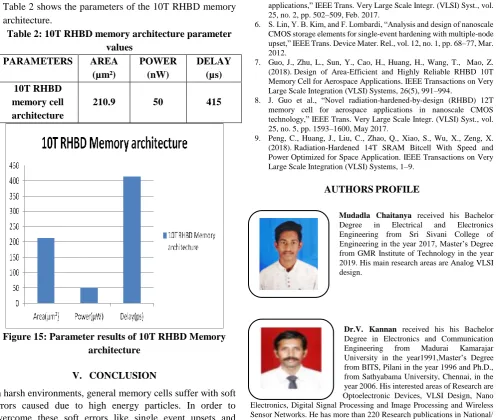
The 10T RHBD memory architecture parameter results are shown in figure 15. The output voltage in 4*4 memory architecture is low when bit and bit bar inputs are at low voltages. When d0 and d3 changes from high to low and low to high, the memory cell’s read operation is observed. In write operation, when the write enable gets on after that the data goes high from low to high and then remains constant, which shows that the data is being read by the memory cell. The 10T RHBD memory architecture parameter values are below shown in table 2.
[image:5.595.319.534.458.712.2]Design And Analysis Of RHBD Memory Cells And 4x4 RHBD 10T Memory Cell Architecture
[image:6.595.53.301.74.401.2]Table 2 shows the parameters of the 10T RHBD memory architecture.
Table 2: 10T RHBD memory architecture parameter values
PARAMETERS AREA
(µm²) POWER (nW) DELAY (µs) 10T RHBD memory cell architecture
210.9 50 415
Figure 15: Parameter results of 10T RHBD Memory architecture
V. CONCLUSION
In harsh environments, general memory cells suffer with soft errors caused due to high energy particles. In order to overcome these soft errors like single event upsets and multiple event upsets, the radiation hardened designs with 10T, 12T and 14T memory cells are used. The performance comparison analysis of single event upsets to multi event upsets, are performed. The use of 10T cell increases the robustness of the memory cell design. Compared all the radiation hardened memory cells, 10T memory cells exhibits less in area, power and delay. A 2 byte RHBD memory is designed using 10T memory cells. This memory architecture can be implemented in any high radiation environment.
REFERENCES
1. E. Ibe, H. Taniguchi, Y. Yahagi, K.-I. Shimbo, and T. Toba, “Impact of scaling on neutron induced soft error in SRAMs from a 250 nm to a 22 nm design rule,” IEEE Trans. Electron Devices, vol. 57, no. 7, pp. 1527–1538, Jul. 2010.
2. C. Boatella, G. Hubert, R. Ecoffet, and S. Duzellier, “ICARE on-board SAC-C: More than 8 years of SEU and MCU, analysis and prediction,” IEEE Trans. Nucl. Sci., vol. 57, no. 4, pp. 2000–2009, Aug. 2003. 3. Sánchez-Macián, P. Reviriego, and J. A. Maestrso, “Combined SEU
and SEFI protection for memories using orthogonal Latin square codes,” IEEE Trans. Circuits Syst. I, Reg. Papers, vol. 63, no. 11, pp. 1933–1943, Nov. 2016.
4. Yan, Z. Huang, M. Yi, X. Xu, Y. Ouyang, and H. Liang, “Double node- upset-resilient latch design for nanoscale CMOS technology,” IEEE Trans. Very Large Scale Integr. (VLSI) Syst., vol. 25, no. 6, pp. 1978–1982, Jun. 2017.
5. R. Giterman, L. Atias, and A. Teman, “Area and energy-efficient complementary dual-modular redundancy dynamic memory for space
applications,” IEEE Trans. Very Large Scale Integr. (VLSI) Syst., vol. 25, no. 2, pp. 502–509, Feb. 2017.
6. S. Lin, Y. B. Kim, and F. Lombardi, “Analysis and design of nanoscale CMOS storage elements for single-event hardening with multiple-node upset,” IEEE Trans. Device Mater. Rel., vol. 12, no. 1, pp. 68–77, Mar. 2012.
7. Guo, J., Zhu, L., Sun, Y., Cao, H., Huang, H., Wang, T., Mao, Z. (2018). Design of Area-Efficient and Highly Reliable RHBD 10T Memory Cell for Aerospace Applications. IEEE Transactions on Very Large Scale Integration (VLSI) Systems, 26(5), 991–994.
8. J. Guo et al., “Novel radiation-hardened-by-design (RHBD) 12T memory cell for aerospace applications in nanoscale CMOS technology,” IEEE Trans. Very Large Scale Integr. (VLSI) Syst., vol. 25, no. 5, pp. 1593–1600, May 2017.
9. Peng, C., Huang, J., Liu, C., Zhao, Q., Xiao, S., Wu, X., Zeng, X. (2018). Radiation-Hardened 14T SRAM Bitcell With Speed and Power Optimized for Space Application. IEEE Transactions on Very Large Scale Integration (VLSI) Systems, 1–9.
AUTHORSPROFILE
Mudadla Chaitanya received his Bachelor
Degree in Electrical and Electronics Engineering from Sri Sivani College of Engineering in the year 2017, Master’s Degree from GMR Institute of Technology in the year 2019. His main research areas are Analog VLSI design.
Dr.V. Kannan received his his Bachelor