electron transistor (SET) structures are investigated by combining 3-D design and SPICE simulation. First, the metal gate is simu-lated by using a 3-D simulator, which enables to design realistic 3-D device structures, and its movement is studied for different design parameters. It is demonstrated that a low stiffness design of the structure is essential for a low-voltage actuation. Results are compared with theoretical numerical simulation and a tunable capacitor model is then embedded in a SPICE simulator and coupled either with a transistor model for MOS-NEMS or with a newly developed SET analytical model for SET-NEMS. It is shown that the use of NEMS membrane can add new function-alities to conventional MOSFET and SET, such as very abrupt switching of the current, which can break theoretical limits of MOSFET, or modulation of Coulomb oscillations governing SET characteristics.
Index Terms—Analytical modeling, metal-oxide-semiconductor field effect transistor (MOSFET), movable gate, nanoelectrome-chanical system (NEMS), single-electron transistor (SET), 3-D modeling.
I. INTRODUCTION
A. Hybrid Circuits Emergence
H
YBRID circuits featuring single-electron transistors (SETs), metal-oxide-semiconductor field-electron-tran-sistors (MOSFETs) and microelectromechanical systems/na-noelectromechanical systems (MEMS/NEMS) are getting increasing interest as very attractive candidates for future low-power and multifunctional nanoscale ICs. Introduction of nanoelectromechanical structures into conventional MOSFETs and SETs may provide superb performance and numerous new functionalities that are not achieved using present devices. In this way, a combination of MEMS and solid-state MOS transistor, which could act as a current switch or as a tunable capacitor, was investigated based on numerical simulation andManuscript received June 9, 2006; revised October 23, 2006. The review of this paper was arranged by Associate Editor T. Hiramoto.
B. Pruvost is with the Quantum Nanoelectronics Research Center, Tokyo Institute of Technology, Tokyo 152-8552, Japan (e-mail: [email protected]. titech.ac.jp).
H. Mizuta is with the Department of Physical Electronics, Tokyo Institute of Technology, and also with SORST, Japan Science and Technology (JST), Tokyo 152-85552 Japan (e-mail: [email protected]).
S. Oda is with the Quantum Nanoelectronics Research Center and the De-partment of Physical Electronics, Tokyo Institute of Technology, and also with SORST, Japan Science and Technology (JST), Tokyo 152-85552 Japan (e-mail: [email protected]).
Color versions of one or more of the figures in this paper are available online at http://ieeexplore.ieee.org.
[image:1.594.346.512.167.248.2]Digital Object Identifier 10.1109/TNANO.2007.891825
Fig. 1. Schematic of a conventional metal–metal capacitor.
analytical modeling [1], [2], and a very recent report experi-mentally demonstrated its virtues [3]. Another recent report also proposed a design combining a nanoscale movable gate and a transistor, which could lower the threshold voltage and enhance the drive current [4]. Similarly, it has also been suggested that variable NEMS capacitor could add new functionalities to conventional SETs such as tunable capacitance [5]. Therefore, the design of the movable gate is essential to achieve the performance predicted by the numerical simulation. However, it cannot be investigated in an efficient manner if not modeled in a 3-D context. In this work, we present different designs of movable electrodes and report expected results based on 3-D calculation and analytical modeling for both MOS-NEMS and SET-NEMS architectures.
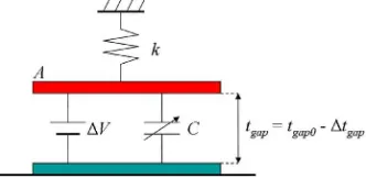
B. NEMS-Gate Devices Principle
The NEMS-gate devices operation is based on the principle of the conventional metal–metal capacitor, i.e., a movable top plate suspended by hinges over a fixed bottom plate, as it is depicted in Fig. 1. By applying a voltage across these two plates, the sus-pended plate starts to continuously move downwards under the influence of the attractive electrostatic force which is in equilib-rium with the elastic force
(1)
where is the plate displacement, the initial air-gap, the overlap area, and the applied voltage between the plates.
Thus, as the top plate deflects vertically, that is as in-creases, the capacitance increases according to
(2)
If is increased to more than , the equilibrium
is broken because of the overwhelming electrostatic force,
Fig. 2. 3-D simulation of a MOS-NEMS membrane with COMSOL [6].
resulting in the snap of the two plates, the theoretical pull-in voltage being
(3)
II. MOSFETS WITH ANEMS-GATE
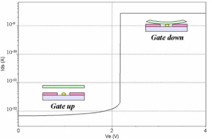
MOS-NEMS devices combine a MOS transistor and a metal membrane suspended over its channel. One of the unique characteristics of these devices is their superexponential de-pendence of the inversion charge versus the gate voltage in the subthreshold region, resulting of the ultra-abrupt movement of the metal membrane. Such devices are expected to break theoretical limits of the solid-state MOSFET such as its subthreshold slope ideal limit of 60 mV/decade. Furthermore, as well as abrupt current switch, applications as molecular or high sensitive DNA sensors are imaginable.
A. 3-D Modeling
The model used to perform 3-D simulation in the Comsol software [6] is depicted in Fig. 2. The gate is made of aluminium and is anchored by four arms on either side of the channel. Each arm is 20 long and 3 large. The inversion layer, which plays the role of the bottom plate of the conventional capacitor switch, is modeled by a simple closed polyline inside of which a constant potential is applied, and has the same area as the metal membrane does.
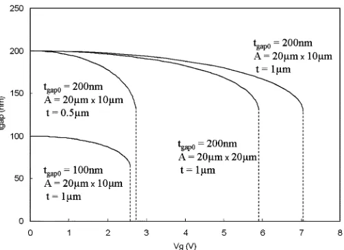
Fig. 3 shows the movement of the gate electrode for var-ious device parameters: initial air gap, gate area, and gate thick-ness. It is important to note that since COMSOL does not per-form contact analysis, the simulation is stopped just before the pull-in effect occurs. As expected by the theoretical formula (3), the pull-in voltage decreases as the initial air-gap and the gate thickness decrease, and as the gate area increases. One can notably notice that the gate thickness has a very important ef-fect on the membrane behavior. This result cannot be quantita-tively provided by the 2-D theoretical model because the spring constant is supposed to represent both the hinges design and the gate stiffness at the same time. It suggests that to achieve
Fig. 3. MOS-NEMS membrane actuation for various parameters: initial air-gapt , areaA, thicknesst.
a low enough pull-in voltage, it may be more efficient to lower the global stiffness of the structure (e.g., by designing appro-priate hinges or by decreasing the gate thickness), rather than increasing the gate area, which would be conveyed by space waste and gate leakage.
B. Implementation in a Circuit Simulation
Electric behavior of the MOS-NEMS device can then be studied by embedding these results in professional simulator SmartSpice [7] by using its Verilog-A interface that allows us to describe one’s own model. The device is divided in two parts: the NEMS part, which describes the movable gate behavior, and the MOS part, which describes the electrical characteristics of the transistor itself.
However, 3-D calculated results are not significant as things are in the MOS-NEMS case, since the potential of the inver-sion layer is considered as constant in this simulation, whereas in reality, the capacitive divider created by the air-gap and the channel oxide means the inversion layer has a feedback on the gate movement according to the following equation:
(4)
where and are, respectively, the gate voltage and the intrinsic gate voltage, and and are the gate-to-channel capacitance and the air-gap capacitance. This effect results in an increase in the pull-in voltage.
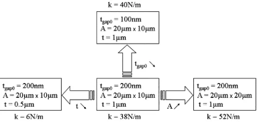
[image:2.594.38.286.73.189.2]Fig. 4. 3-D dependence of the equivalent spring constantkwith initial air-gap
t , areaA, and thicknesst.
Fig. 5. Reproduction of the theoretical model using the equivalent spring con-stant (solid line) with the initial 3-D simulated results (dotted line).
results. The reproduction is quite good because the gate design is very similar to the theoretical parallel-plate model.
Finally, the continuous expression of the gate-to-channel ca-pacitance proposed in [1] is also used
(5)
where , , and , respectively, the oxide
and depletion capacitance, the intrisic threshold voltage, and the thermal voltage.
Concerning the MOS part, BSIM model [8], available in SmartSpice library, is used to describe the electrical character-istics of the transistor. Note that the oxide thickness is supposed to be equal to 40 nm.
The two parts are then combined in an usual SPICE netlist, and the simulation is performed at low drain voltage
.
[image:3.594.306.554.66.237.2]Fig. 6 shows that the abrupt movement of the gate results in a switching of the MOSFET drain current. This suggests that the steepest transition between on and off states of a conven-tional MOSFET (60 mV/decade) can be improved by the use of the NEMS-gate. However, it is important to note that the ex-perimentally observed transition may strongly differ from the one depicted in the figures since the SPICE electrical simulation does not take into account the mechanical limitations inherent
Fig. 6. MOS-NEMS drain currentI versus gate voltageV (in log-lin scale) at low drain voltageV = 50 mVfor different structures.
to the displacement of the metal gate. As already mentioned, the 3-D simulation is stopped just before the pull-in effect oc-curs, preventing us to investigate the speed of the gate move-ment. Nevertheless, according to simple mechanical consider-ations, we can easily affirm that the lower the stiffness of the structure, the speediest the switching and as already told, the lower the pull-in voltage. Thus, it is essential to achieve a struc-ture as supple as possible for switching application. Another handicap is the friction due to the air-gap between the gate and the channel. One possible solution is to operate the device in vacuum.
III. SINGLE-ELECTRONTRANSISTORSWITH ANEMS-GATE
The concept of a movable gate can be extended to the case of the SET, as it was suggested in [5]. By tuning the gate ca-pacitance of the SET, one can change the total island capaci-tance and, hence, control the periodicity and the level of the cur-rent. NEMS-gate architectures could also enrich conventional SETs with new functionalities such as threshold gate behavior or abrupt current switching, and in a general manner, further control of the device’s behavior.
A. Set Analytical Model
Simulation of hybrid circuits featuring SETs in a SPICE environment is fairly difficult because of the electrical char-acteristics of SET that result from the Coulomb blockade phenomenon. Accurate but time-consuming Monte Carlo sim-ulations are not adapted to design realistic circuits featuring a large number of components. Therefore, accurate SET analyt-ical models are required to allow faster simulations. We propose a physically based compact SET analytical model for hybrid simulation. This model is based on the “orthodox” theory of single charge tunneling and the master equation method [10], [11]. The model is verified against the simulated data from Monte Carlo simulator CAMSET [9]. It describes accurately SET characteristics for a wide range of drain to source voltages
( , where is the total island capacitance)
and temperatures . The proposed model
[image:3.594.47.286.223.384.2]Fig. 7. I 0V verification of our model for symmetric device withC =
[image:4.594.51.279.65.226.2]0:2 aF,C = C = 0:15 aF, andR = R = 1 MatT = 173 K. Here, the dotted line represents master equation simulation (CAMSET) [9] and solid line represents our model.
Fig. 8. I 0 V verification of our model at different temperature levels for symmetric device withC = 2 aF,C = C = 1 aF, andR = R =
1 M. Here, the dotted line represents master equation simulation (CAMSET) [9] and solid line represents our model.
to source voltages. Fig. 8 shows several drain currents obtained at different temperature levels (from 50 to 500 K),
with and without background charge. Impact of
temperature on the Coulomb blockade can be clearly seen: it disappears when the temperature increases. It can be noted that our model is in perfect accordance with CAMSET simulation. Actually, the domain of validity of our model does not depend on the temperature (until 500 K). We also verified it for several capacitances values, and the same performances were observed.
Our model has been validated until . To the
best of our knowledge, the best analytical model reported until now is the MIB model [5] which is valid for
but only for low temperatures .
B. 3-D Modeling
Fig. 9 shows the beam structure used to simulate the gate. It is made of aluminium and is suspended over the substrate. A nanowire SET (70 nm 2 ) is designed under the beam, but for simplification, its potential is considered as constant. It is worth noting that, contrary to the case of MOS-NEMS, the
Fig. 9. 3-D simulation of a SET-NEMS beam with COMSOL [6].
Fig. 10. SET-NEMS gate actuation according to the actuated electrode.
two facing actuation electrodes, i.e., the gate electrode and the buried electrode, do not have the same area. Because of this dis-symmetry, the gate behavior will be different according to the electrode which is chosen as actuation electrode, as shown in Fig. 10. It can be assumed that a lower pull-in voltage is needed when the movable gate is actuated because of its wider area which contributes more to the electrostatic force. Fig. 11 shows electrostatic actuations for different parameters: initial air-gap, gate length, gate thickness, and gate material (one layer Al, or two layers Al/ ). As predicted by the theoretical formula (3), the pull-in voltage decreased as the initial air-gap or the thick-ness decreases and as the length increases. It is worth noting that the equilibrium region can be extended beyond the theoretical value by the use of a layer underneath a thin con-ductive layer (in this case, a 50-nm-thin aluminium layer), to the price of a substantial increase in the pull-in voltage, due to the in-series connection of the oxide and gap capacitances.
[image:4.594.302.550.231.400.2] [image:4.594.48.282.290.448.2]Fig. 11. SET-NEMS gate actuation for various parameters: initial air-gap
[image:5.594.304.554.67.191.2]t , gate areaA, thicknesst, and material.
Fig. 12. 3-D simulation of a SET-NEMS movable gate with COMSOL [6].
Fig. 13. SET-NEMS gate actuation for different overlap areas.
the square root of the gate area, as suggested by the theoret-ical formula (3), even though the design of the structure differs from the parallel-plate theory. It can be assumed that the sur-face of the gate notvis-a-visthe buried electrode (i.e., the bridge and the hinges) has only little influence on the evolution when increasing the area in this manner. Moreover, it also suggests that an unreasonable increase in area is not efficient to achieve
Fig. 14. (a) Electrical equivalent circuit of SET-NEMS device. (b) Displace-ment of the movable gate(G2)(left axis) and corresponding capacitanceC (right axis) versus actuation voltageV 0 V .
Fig. 15. SET-NEMS drain to source currentI versus gate 1 voltageV . SET device parameters areC = 0:15 aF,C = C = 0:1 aFandR =
R = 1 M,V = 0 V,V = 0:03 VatT = 173 K.
a pull-in voltage less than , since an area of 80 , i.e., 20 times larger than the initial one, would be needed in this con-figuration.
C. Implementation in a Circuit Simulation
Electrical behavior of the device is then investigated by coupling the 3-D calculated results and the proposed analytical model in SmartSpice. The device corresponding to the electrical equivalent circuit depicted in Fig. 14(a) is studied. It possesses two gates: a buried gate , that acts as a normal gate, and a movable gate , which is the one depicted in Fig. 12. This gate has a total overlap area of 16 with the buried electrode and enables it to tune the total island capacitance of the SET. Its displacement is modeled by using an empirical poly-nomial and embedded thanks to Verilog-A. The displacement of the gate and the corresponding capacitance is shown in Fig. 14(b). is simply calculated as equal to the in-series connection of and , respectively, corresponding to the air-gap capacitance and to the oxide capacitance of a supposed 20-nm-thin layer covering the region underneath the movable gate.
[image:5.594.298.556.244.374.2] [image:5.594.42.288.310.446.2] [image:5.594.42.290.477.646.2]Fig. 16. SET-NEMS drain to source currentI versus gate 2 voltage,V . SET device parameters areC = 0:15 aF,C = C = 0:1 aFandR =
[image:6.594.58.274.257.399.2]R = 1 M,V = 0:2 VatT = 173 K.
Fig. 17. SET-NEMS drain to source current I versus buried electrode voltageV (in log-lin scale). SET device parameters areC = 0:15 aF,
C = C = 0:1 aFandR = R = 1 M,V = 0:03 V,V = 0 V,
V = 0:03 VatT = 173 K.
Fig. 18. (a) Schematic of a SET-NEMS inverter whose inversion threshold can be switched between two values. (b) Switching of the inversion threshold. Here, parameters of SET devices areC = 3 aF,C = C = 1 aFandR =
R = 1 M,C can be switched between 0.5 aF and 1 aF (i.e.,1=6C and
1=3C ),V = 0:02 V,C = 1 fFatT = 10 K.
the fact that the period is equal to in this case. However, if the movable gate is activated, the periodicity of the os-cillations, then equal to , can be switched between two different values. Such periodicity encoding of the current could be used in a communication system to get rid of the unwanted background charge effect. Another interesting feature of this de-vice is that the current level can also be controlled as shown in Fig. 17, so that the device can also be used as a current switch
NEMS could be integrated in multifunctional neuron cells able to involve only very few devices, and neural networks inheriting at the same time the SET ultra-low power consumption.
IV. CONCLUSION
We have studied both NEMS-gate MOSFET and SET struc-tures by combining 3-D design and a newly developed SET an-alytical model. Our hybrid simulation has enabled us to inves-tigate new functionalities that could be added to conventional MOSFET and SET such as very abrupt current switching, and in a general manner further control of the device’s behavior.
ACKNOWLEDGMENT
The authors would like to thank Dr. S. Saito and Dr. T. Arai of Hitachi Central Research Laboratory and Dr. T. Shimada of Quantum 14 Company, Ltd., for their valuable discussion.
REFERENCES
[1] A. M. Ionescu, V. Pott, R. Fritschi, K. Banerjee, M. J. Declercq, P. Re-naud, C. Hibert, P. Fluckiger, and G. A. Racine, “Modeling and design of a low-voltage SOI suspended-gate MOSFET (SG-MOSFET) with a metal-over-gate architecture,” inProc. ISQED, 2002, pp. 496–501. [2] N. Abelé, V. Pott, K. Boucart, F. Casset, K. Segueni, P. Ancey, and
A. M. Ionescu, “Comparison of RSG-MOSFET and capacitive MEMS resonator detection,”Electron. Lett., vol. 41, no. 5, pp. 242–244, 2005. [3] N. Abelé, R. Fritschi, K. Boucart, F. Casset, P. Ancey, and A. M. Ionescu, “Suspended-gate MOSFET: Bringing new MEMS func-tionality into solid-state MOS transistor,” inProc. IEDM, 2005, pp. 479–481.
[4] H. Kam, D. T. Lee, R. T. Howe, and T.-J. King, “A new nano-electro-mechanical field effect transistor (NEMFET) design for low-power electronics,” inProc. IEDM, 2005, pp. 477–480. [5] S. Mahapatra, V. Vaish, C. Wasshuber, K. Banerjee, and A. M. Ionescu,
“Analytical modeling of single electron transistor (SET) for hybrid CMOS-SET analog IC design,”IEEE Trans. Electron. Devices, vol. 51, no. 11, pp. 1772–1782, Nov. 2004.
[6] COMSOL, User’s guide. [Online]. Available: www.comsol.com [7] SmartSpice, User’s guide. [Online]. Available: www.silvaco.com [8] Y. Caoet al., “New paradigm of predictive MOSFET and interconnect
modeling for early circuit design,” inProc. CICC, 2000, pp. 201–204. [Online]. Available: www.eas.asu.edu/~ptm
[9] M. Kirihara, K. Nakazato, and M. Wagner, “Hybrid circuit simulator including a model for single electron tunneling devices,”Jpn. J. Appl. Phys., vol. 38, pp. 2028–2032, 1999.
[10] H. Grabert and M. Devoret, “Single Charge Tunneling,” inSeries B: Physics, ser. NATO ASI Series. New York: Plenum Press, 1992, vol. 294.
[11] K. K. Likharev, “Single-electron devices and their applications,”Proc. IEEE, vol. 87, no. 4, pp. 606–632, 1999.
[image:6.594.40.291.467.593.2]Hiroshi Mizuta(M’89) was born in Kochi, Japan, in 1961. He received the B.S. and M.S. degrees in physics and the Ph.D. degree in electrical engineering from Osaka University, Osaka, Japan, in 1983, 1985, and 1993, respectively.
He joined the Central Research Laboratory, Hitachi Ltd., Tokyo, Japan, in 1985, and has been engaged in research on high-speed heterojunction devices and resonant tunneling devices. From 1989 to 1991, he worked on quantum transport simula-tion, and also from 1997 to 2003, he worked on single-electron devices and other quantum devices as the Laboratory Manager and Senior Researcher at the Hitachi Cambridge Laboratory, Cambridge, U.K. Since 2003, he has been an Associate Professor of Physical Electronics at the Tokyo Institute of Technology. He has coauthored more than 200 scientific papers and filed over 50 patents. He has also coauthored books and chapters, in-cludingPhysics and Applications of Resonant Tunnelling Diodes, (Cambridge
physics, and the M.S. and Ph.D. degrees from the Tokyo Institute of Technology, Tokyo, Japan, in 1974, 1976 and 1979, respectively.
He is a Professor in Department of Physical Electronics and Quantum Nanoelectronics Research Center, Tokyo Institute of Technology. He has authored more than 200 papers published in journals and conference proceedings. His current research interests include fabrication of silicon quantum dots by pulsed plasma processes, single electron tunneling devices based on nanocrystalline silicon, ballistic transport in silicon nanodevices, silicon-based photonic devices, and high-k gate oxide ultrathin films prepared by atomic layer MOCVD.

![Fig. 12. 3-D simulation of a SET-NEMS movable gate with COMSOL [6].](https://thumb-us.123doks.com/thumbv2/123dok_us/8496084.346006/5.594.42.288.310.446/fig-d-simulation-set-nems-movable-gate-comsol.webp)