10-19-2018
An Etching Study for Self-Aligned Double
Patterning
Christopher O'Connell
[email protected]Follow this and additional works at:https://scholarworks.rit.edu/theses
This Thesis is brought to you for free and open access by RIT Scholar Works. It has been accepted for inclusion in Theses by an authorized administrator of RIT Scholar Works. For more information, please [email protected].
Recommended Citation
Christopher O’Connell
October 19,2018
A Thesis Submitted in Partial Fulfillment
of the Requirements for the Degree of Master of Science
in
Microelectronic Engineering
in Partial Fulfillment
of the Requirements for the Degree of Master of Science
in
Microelectronic Engineering
Committee Approval:
Dr. Robert Pearson Advisor Date
Program Director, Microelectronic Engineering
Dr. Karl Hirschman Date
Professor, Electrical and Microelectronic Engineering
Dr. Michael Jackson Date
Professor, Electrical and Microelectronic Engineering
Dr. Sohail Dianat Date
Deptartment Head, Electrical and Microelectronic Engineering
DEPARTMENT OF ELECTRICAL AND MICROELECTRONIC ENGINEERING KATE GLEASON COLLEGE OF ENGINEERING
ROCHESTER INSTITUTE OF TECHNOLOGY ROCHESTER, NEW YORK
I would like to thank and acknowledge everyone who has helped and supported me
through-out this process. Firstly, I would like to thank my committee members, Dr. Robert
Pear-son, Dr. Karl Hirschman and Dr. Michael Jackson for all their support and guidance
throughout my time at RIT. A special thanks to Dr. Hirschman and the many members
of Team Eagle over the years many of whom taught me a great number of things and
trained me on tools. It was a pleasure to work with the SMFL Staff, Bruce Tolleson,
Rich Battaglia, Zachary Kogut, Sean O’Brien, Scott Blondell and last but certainly not
least Patricia Meller and John Nash. A special thanks goes to Patricia for our many
conversations over the years about a variety of things but largely for helping me out when
I needed it most and teaching me to be the process engineer I am today. Without John
this project would have failed before it had started, beyond that his insights into how
tools are intended to be run and how to diagnose process problems from tool problems as
well as life advice has been invaluable. A very special thanks to Emily Shriver, for letting
me stay at her apartment significantly longer than a month, being patient and putting
up with me for the past year and few months. I would also like to thank Jeff Salzmann
for his life advise and helping me with interviewing and career advice. I would also like to
thank the grad office both old and new for their thoughtful discussions and being there
for me when I needed to work something out, especially Venkatesh Deenadayalan who has
listened to way too many of my ramblings and helped me work through problems I was
stuck on. Lastly to all my family and friends I’ve made along the way I want to thank you
selectivity and anisotropy. The proposed process flow was developed at RIT, designed to
closely reproduce what the semiconductor industry uses for a Self-Aligned Double
Pattern-ing (SADP) process module while advancPattern-ing RIT’s current cleanroom facility capabilities.
The etching experiment is proposed such that a sufficient degree of etch endpoint
control can be achieved without a spectrophotometer for endpoint detection using the
Magnetically Enhanced Reactive Ion Etching (MERIE) system at RIT. Without the proper
etch data a number of critical steps would be incredibly difficult to control. Prior to this
work across wafer etch non-uniformity was reported to be approximately 10% with a
regular rate of 1400-1500A min−1. This was improved through various means to a
non-uniformity of<1% and a rate of 2200A min−1 on average. A way to achieve the mandrel
etch and strip using gas ratios of 4:2:1::CF4 :CHF3 :C2F6 and 4:1::CHF3 :C2F6 , was
Signature Sheet
Abstract ii
Table of Contents iii
List of Figures vi
List of Tables ix
List of CVD and RIE Symbols x
List of Anisotropy and Selectivity Symbols xii
1 Motivation for a Patterning Etch Study 1
2 Theory 4
2.1 Lithography . . . 4
2.1.1 Litho-Etch-Litho-Etch . . . 5
2.1.2 Self-Aligned Double Patterning . . . 6
2.2 Plasma Processing . . . 7
2.2.1 Chemical Vapor Deposition . . . 11
2.2.2 Reactive Ion Etching . . . 19
3 Process Flow and Experimental Investigation 34
3.1 Process flow . . . 34
3.1.1 SOC Fin Hardmask Deposition . . . 35
3.1.2 Oxide Mandrel Deposition . . . 35
3.1.3 BARC Deposition . . . 36
3.1.4 Resist Coat, Expose and Develop . . . 37
3.1.5 BARC Open and Trim Etch . . . 37
3.1.6 Mandrel Etch . . . 38
3.1.7 PECVD Nitride Deposition . . . 39
3.1.8 Nitride Spacer Etch . . . 40
3.1.9 Mandrel Strip . . . 40
3.1.10 SOC etch . . . 41
3.1.11 Silicon Fin Etch . . . 42
3.2 Etch Rate, Anisotropy and Selectivity Study of Oxide Etching . . . 42
4 Film Uniformity and Etching 45 4.1 Spin-On Glass (SOG) and Tetraethyl orthosilicate (TEOS) uniformity . . 45
4.2 TEOS Etching . . . 47
References 58
A RIT Standard Deposition Recipes 66
B RIT Etch Recipes 67
C Etch Test Photomask details 69
C.1 Aspect Ratio Dependant Etching . . . 70
1.1 Planar vs FinFET . . . 2
1.2 Double Pattterned FinFET formation . . . 3
2.1 LELE simplified flow . . . 5
2.2 LELE overlay issues . . . 6
2.3 SADP simplified flow . . . 6
2.4 SADP cut mask . . . 7
2.5 Plasma Technology . . . 8
2.6 C-V chart for glow discharge plasmas . . . 8
2.7 Plasma Reactions . . . 9
2.8 Paschen curve for voltage breakdown . . . 10
2.9 CVD Reaction Chambers . . . 12
2.10 Plasma Reactions Deposition . . . 12
2.11 Film growth . . . 13
2.12 Gibbs Energy vs Temperature Curve . . . 15
2.13 Reynolds and Grashof reactor profiles . . . 16
2.14 Void formation . . . 17
2.15 RIE reactors . . . 19
2.17 RIE effects . . . 23
2.18 Etching feature size specifications . . . 24
2.19 Mask erosion . . . 25
2.20 MERIE reactor . . . 27
2.21 B-field trajectory . . . 27
2.22 Stages of spin coating . . . 28
2.23 Spin coating fluid evaporation . . . 29
2.24 Spin coating evaporation surface . . . 29
2.25 Sol-Gel/St¨ober Process for TEOS . . . 30
2.26 TEOS-ethanol-water system . . . 31
2.27 Carbon ternary phase diagram . . . 32
2.28 Spin On Carbon Monomers . . . 33
3.1 SOC Fin Hardmask Deposition . . . 35
3.2 Oxide Mandrel Deposition . . . 36
3.3 BARC Deposition . . . 36
3.4 Resist Coat, Expose and Develop . . . 37
3.5 Bottom Anti-Reflective Coating (BARC) Open and Trim . . . 38
3.6 Mandrel Etch . . . 39
3.7 PECVD Nitride Deposition . . . 40
3.8 Nitride Spacer Etch . . . 40
3.9 Mandrel Strip . . . 41
4.1 SOG coating . . . 46
4.2 MERIE Chamber Showerhead . . . 48
4.3 MERIE Chamber Chuck . . . 49
4.4 Resist Reticulation . . . 50
4.5 Ternary plot of Rate Data . . . 53
4.6 Ternary plot of Uniformity Data . . . 53
4.7 C2F6 vsCHF3 . . . 54
5.1 Self-Aligned Quadruple Patterning (SAQP) . . . 57
C.1 ARDE Design . . . 70
C.2 ARDE SEM image . . . 70
C.3 Microloading Design . . . 71
3.1 Enchant selectivity test Parameters Table . . . 44
4.1 SOG Uniformity . . . 46
4.2 TEOS Uniformity . . . 47
4.3 Preliminary etch results . . . 50
4.4 Polymer Descum . . . 51
A.1 RIT Standard PECVD TEOS Recipie . . . 66
B.1 RIT Old Standard Anisotropic Oxide Etch . . . 67
B.2 RIT New Standard Anisotropic Oxide Etch . . . 67
B.3 Mandrel Etch . . . 67
Term Description Units/Value
ai Thermodynamic concentration
ai(eq) Thermodynamic concentration at equilibrium
DA Radical diffusion coefficient m3s−3
Da Ambipolar diffusion coefficient m3s−3
d Electrode separation distance cm
G Gibbs free energy J
Grt Grashoff’s number (thermal) 10−2 ≤102(APCVD)/
0≤10(LPCVD)
g Gravitational constant 9.8m s−2
H Enthalpy J
Kn Knudsen number 10−6 ≤10−5(APCVD)/
10−3 ≤10−2(LPCVD)
L Characteristic length m
nA Radical density m−3
ni Ion density m−3
nmat Particle Density m−3
p Pressure Pa
Re Renyolds number 10−2 ≤102
S Entropy J K−1
srec Solid recombination probability
T Temperature K
Tr Reference Temperature K
U Internal Energy J
V Volume m3
V Voltage V
v Velocity m s−1
¯
v Average speed m s−1
α Townsend Coefficient # ions m−1
i
η Viscosity Pa s
λ Mean free path length m
Term Description Units/Value
A Anisotropy (0≤1)
Am Mask anisotropy (0≤1)
B Undercutting Bias (0≤1)
dc Minimum resolvable mask feature size/ µm
Critical dimension (space)
df Desired feature size upper width µm
dm Mask dimension(line) µm
dP itch Mask pitch µm
Rf Film etch rate µm s−1
Rh Horizontal etch rate µm s−1
Rv Mask erosion rate, Vertical etch rate µm s−1
Rv,ave Average Rv µm s−1
Rs Substrate erosion rate µm s−1
Sfm Selectivity of the mask to the film (0≤1)
Sf
s Selectivity of the film to the substrate (0≤1)
tc Time to clear s
tmin Time until the substrate is first exposed s
to the plasma
ttot Total etch time s
Um
f Uniformity factor for the film to the mask (0≤1)
Usf Uniformity factor for the substrate to film (0≤1)
yf Film thickness µm
ys,max Substrate max etch depth µm
α Film thickness variation (0≤1)
β Film etch uniformity/variation (0≤1)
∆ Mask erosion µm
δ Overetching parameter (0≤1)
Mask erosion rate variation (0≤1)
RIT has been teaching students about IC fabrication since the program’s
in-ception in 1982, the introduction of the masters program in 1987 and its student-run
factory in 1988 [1–3]. In 1992 RIT accomplished a longterm goal of producing CMOS
circuits for its factory class with a P-Well 9 photolithographic layer process and single level
metal [1, 4]. This process was refined not much later in 2000 into a sub-micron process
producing an Lef f < 1.0µm process with 10 lithographic levels and the introduction of
a second metal layer [5, 6]. This process was then refined again to produce 250nm
tran-sistors in 2006 [7]. In 2014 this process was brought down to a 150nm advanced CMOS
with a 14 level lithographic process [8–10].
In recent years industry has moved away from a planar structure, as shown in
Figure 1.1a, that RIT has been using, and has moved to the FinFET device architecture
as shown in Figure 1.1b [11, 12]. This is largely in part due to Moore’s law moving the
industry to make smaller and smaller transistors improving packing density. With this new
development also comes larger control with the process, with planar devices the active
area is simply L∗W, however the active area in a FinFET is L∗(t+ 2∗Hf in)this allows
for the transistor width to be dependent on height and minimally the width of the fin
(a) (b)
Figure 1.1: Two types of MOSFET: Planar FET(a) and FinFET(b) [11].
With this recent development in industry RIT is looking to further develop its
CMOS process into a FinFET process. This has been attempted before at RIT using Low
Temperature Oxide (LTO) sidewall spacers with a pitch of 0.5-1µm between fins [13–15].
While the process is sound, it doesn’t have the appropriate packing density to call it a
FinFET process. In order to continue forward, sub-lithographic patterning techniques,
such as double patterning, need to be introduced.
There are multiple ways to go about sub-lithographic patterning primarily
Litho-Etch-Litho-Etch (LELE), Litho-Freeze-Litho-Etch (LFLE) and Self-Aligned Double
Pat-terning (SADP), these three techniques have been used at RIT with varying success
[16–19]. As opposed to LELE and LFLE this work will primarily focus on SADP as a
viable method for double patterning, primarily as it is likely to be the most expandable for
a quadruple or even octuple patterning process. In the SADP process one of the key
chal-lenges is having a appropriate etch and deposition control as opposed to the lithographic
concerns. A highly simplified SADP process is is depicted in 1.2 for the formation of a
fin.
Without adequate hardmask and spacer definition etch processes, SADP
1 2 3
Figure 1.2: Simplified FinFET formation through SADP.
1.2, steps 1 and 2, whereas the hardmask problem is depicted primarily in step 3. For the
fin-definition (step 3) a highly anisotropic etch must be performed to produce at least a
1:3 to 1:5 ratio fort:Hf in (fin aspect ratio, as defined in Figure 1.1b). This requires that
a highly selective and robust hardmask etch process be utilized. RIT has followed various
industry practices in developing our own process for using carbon as a hardmask, be-it
a-carbon/diamond-like carbon or Spin-On Carbon (SOC) [20, 21]. In order to further
im-prove the RIT capabilities through development of a SADP process, both deposition and
etching improvements must be accomplished to achieve a fin etch for FET construction.
On the etch side of the process development significant studies of the oxide, hardmask,
nitride and silicon etch capabilities all need to be carried out, each of which must address
target material etch rate, etch selectivity, etch anisotropy and uniformity. A particular
fo-cus of this work is the oxide etch issues which appear in multiple steps within the process,
namely in the mandrel etch and the mandrel removal explored in further detail in sections
2.1
Lithography
Semiconductor technology is driven by producing ever smaller features.
Reduc-ing the source wavelength is the easiest method of achivReduc-ing smaller features. Originally
industry intended to switch to an Extreme Ultraviolet (EUV) source with a 13.5 nm
wave-length past the 193 nm node. Due to significant complications in the majority of steps in
implementation as well as cost EUV has however been in perpetual development. As such
to continue Moore’s Law steps needed to be taken to produce smaller features without
changing the source. Many ways have been developed such as Phase Shift Mask (PSM)
and Optical Proximity Correction (OPC) but they only went so far. Even those techniques
have stopped producing smaller features, new techniques needed to be developed. This
is where Multiple patterning strategies have been conceived. Of these, two have become
dominant to produce smaller features, LELE and SADP or variants thereof. The
over-all idea is to reduce the half-pitch(the length of line or space within a given pitch) to
sub-wavelength levels through means of further lithography deposition and etching
pro-cesses. SADP combines conventional optical lithography with deposition and etch steps
2.1.1 Litho-Etch-Litho-Etch
LELE is a lithography process where a pattern is formed from multiple patterning
and direct etching steps. Both dense and isolated features can be formed from this
tech-nique. Generally metals with different etch properties such as aluminum and molybdenum
are used as a hardmask, but other materials can also be used [17]. Figure 2.1 depicts a
simplified process flow for LELE to produce dense 1:1 line:space features. As shown in
1 2 3
4 5 6
Figure 2.1: LELE Dense process flow(1:1) [17]
Figure 2.1, the general concept is to deposit the primary hardmask with a secondary
hard-mask above, depicted in Figure 2.1(1). Then photoresist is applied and patterned at a 1:3
line:space ratio to pattern the top hardmask as shown in Figure 2.1(2-3). Following this,
more photoresist is applied and patterned again at the same pitch but with the line placed
in the middle of the previous space as shown in Figure 2.1(4). This new photoresist layer
and the top hardmask then are used to pattern the primary bottom hardmask as shown in
Figure 2.1(5), where the top hardmask and photoresist are then removed leaving only the
bottom hardmask as shown in Figure 2.1(6) [17, 22–24]. While LELE can produce good
results, it can also introduce overlay issues as shown in Figure Figure 2.2 [24, 25]. Most
Figure 2.2: LELE overlay issues for a 1:1 features, following step 3 in Figure 2.1
2.1.2 Self-Aligned Double Patterning
SADP is also a lithography based process by which a pattern is made over
mul-tiple steps that introduces new deposition and etch related issues affecting the line:space
ratio not found in LELE, but none of the overlay issues. SADP does require a second
cut or block mask to clean up the final image when the process is complete in most
circumstances. The SADP process starts by patterning a mandrel as depicted by the top
level of Figure 2.3 forming the primary pattern. The mandrel is then trimmed through
Primary Pattern Secondary Pattern
Spacer Mandrel
Figure 2.3: SADP simplified flow [26]
means of over-development or overetch and a different film is deposited over and etched
back forming spacers on the sidewalls of the mandrel. The mandrel then gets stripped
[image:21.612.199.442.356.602.2]being defined as the secondary pattern [26]. Then a cut or trim mask can be used to
clean up the features as depicted in Figure 2.4. This is a required step as the spacers are
formed around the mandrel and may produce some artifacts that need to be removed in
order for shorts or other defects to not occur [24, 26]. As features have gotten smaller
SADP has been used in conjunction with a-carbon or newer SOC materials to incorporate
etch stops as well as hardmask/BARC layers into the process. The incorporation of these
newer materials has also removed the majority of standing wave effects in resist as a
problem during subsequent etch processes [24, 26–31]. Additionally the use of dry plasma
processing as opposed to wet chemical etching improved the resulting patterned profile.
(1) (2)
Figure 2.4: SADP cut mask before(1) and after(2) [26].
2.2
Plasma Processing
Plasma processing has had a long history within the semiconductor industry in
both coating and etching materials. In plasma processing whether depositing or etching
the primary mechanisms are the same. The various types of coating and etching that are
used within industry are depicted in Figure 2.5. What isn’t listed is that ion implantation
is a plasma process similar to Ion Beam Coating (IBC). The most common processes are
Plasma-Enhanced Chemical Vapor Deposition (PECVD) and sputtering for coating. The
primary focus here is on glow discharge plasmas, specifically for PECVD and Reactive Ion
Etch (RIE). A glow discharge plasma is created by inducing an electric field between an
(a) (b)
Figure 2.5: Types of plasma coating(a) and etching(b) technology [32].
current also known as a Capacitively Coupled Plasma (CCP). All of this is done to achieve
the proper current density in the normal glow region of 10−5 → 10−3A/cm2 as shown
in Figure 2.6. To start the plasma, an electric field between an anode and cathode of
Figure 2.6: Current-Voltage relation for plasma activation [33]
distance d is induced in the chamber, where the field is measured simply as V /d. The
electrons present accelerate towards the anode ionizing a gaseous atom and producing
another electron in the process. This ion then accelerates towards the cathode due to
the induced electric field [33, 34]. If the ion strikes the cathode at sufficient energy a
Figure 2.7: Plasma reaction mechanisms [35]
It then follows that continued collisions produce further collisions eventually
resulting in a breakdown voltage, also shown as sheath voltage, as shown in Equation 2.1c,
wherepis pressure in Torr,dis some distance in cm depicting the plasma sheath edge,γse
is the secondary electron emission coefficient, and A, B and C represent experimentally
derived constants for a particular gas. The current going to the anode is shown as Equation
2.1a, where α is taken to be the Townsend coefficient shown in Equation 2.1b, and λe
is the mean free path length for inelastic(ionization) electron-neutral collisions, E is the
induced electric field, andViis the ionization potential for the gas species. The breakdown
voltage shown in Equation 2.1c can be plotted as a function of the pressure and distance
to produce what is known as a Paschen curve(Vb(pd)) whose minima isVminas depicted
by Figure 2.8.
Icexp(αx) =I (2.1a)
α= 1 λe exp Vi eEλe
≡pAexp −Bp E (2.1b) A(pd)
C+ ln(pd) uVb=
Bpd
lnApd−ln[ln(1 + 1/γse)]
Figure 2.8: A example Paschen Curve depicting the breakdown voltage of a gas between two electrodes separated by a distancedat a pressure p [33]
A Paschen curve exists for every different gas species and cross-section
ioniza-tion [33, 34]. Before the breakdown voltage is achieved the plasma is in the Townsend
region(below 8∗10−5A/cm2 = I
A) once the breakdown voltage is reached a plasma is
said to have ignited and be in the normal glow discharge state, also resulting in a drop in
overall voltage as depicted by Figure 2.6. As the discharge increases there is a change from
the normal glow to abnormal glow used for processing within the cathode sheath [33, 34].
After the plasma is ignited and stable it follows that there is a standard set of chemical
reactions that occur, these are shown by Reactions 2.2a through 2.2i, all of which depict
both the deposition and etching mechanisms, as shown in Figure 2.7 [34–36].
Electron−Ion P air P roduction: e+AB→AB++ 2e (2.2a)
Radical P roduction: e+AB →e+A+B (2.2b)
N egitive Ion P roduction:e+AB→A−+B (2.2c)
Electron Af f inity: A(g) +e→A−(g) (2.2d)
Ion T ransport f lux to surf ace: Γi =−Da∇ni (2.2f)
Radical T ransport f lux to surf ace: ΓA=−DA∇nA (2.2g)
Surf ace Reaction : A(g) +B(s)→C(g) (2.2h)
Ionization Reaction: A(g)→A+(g) +e (2.2i)
Seeing as deposition and etching have their own quirks it is prudent to describe the
reactions that are common for both. As noted before electrons interact with the gases
within the chamber, this is shown in Reactions 2.2a through 2.2d, being electron-ion
pair, radical, negative ion productions and electron affinity respectively. These reactions
produce the ions and radicals that proceed towards the substrate, as depicted by the
Fluxes 2.2f and 2.2g. Once the atoms reach the surface the Reaction 2.2h occurs with
the creation of adsorption sites with the promotion of new gas species as depicted by
Figure 2.7(4). The adsorption site at (4) also alters the film sometimes detrimentally
inducing damage as shown in Figure 2.7(8). Both (4) and (8) do however promote film
adhesion and further reactions as well as desorption. Sputtering as shown in Figure 2.7(5)
can remove species that are trapped or have a low vapor pressure as well as smooth surface
topography. Ion implantation also occurs under this mechanism as referenced by Figure
2.7(6) which also creates defects such as trapped gas species as in Figure 2.7(9) [35]. All
of these reaction processes are manipulated later in this thesis through the use of Chemical
Vapor Deposition (CVD) and RIE to achieve the desired features.
2.2.1 Chemical Vapor Deposition
CVD is a process by which a material is deposited by introducing gases into a
chamber and producing a chemical reaction. This method of thin film deposition produces
a conformal coating as opposed to similar Physical Vapor Deposition (PVD) methods.
products to the substrate surface.
(a) (b) (c)
Figure 2.9: CVD horizontal(a), vertical(b), and pancake(c) reaction chambers [33]
All CVD reactions follow a fundamental transport mechanism as depicted in
Figure 2.7, replicated here in Figure 2.10, however a plasma is not necessarily required, as
higher temperatures are usually used to overcome the∆U,∆Sand∆H or internal energy,
entropy and enthalpy in the reaction, respectively. In CVD the reaction mechanism is most
Figure 2.10: Plasma reaction mechanisms, replicated here from Figure 2.7 [35]
commonly seen to be at the sites (1-5) as shown in Figure 2.7. The first step is depicted
in Figure 2.7(4) following standard plasma processes, then the atoms are diffused along
preferred orientations [33,35,36]. Following surface diffusion comes nucleation and growth
where the film densifies as well as rearranges bonds and modifies film stresses. This is best
depicted by Figure 2.11, which depicts island, layer and Stranski-Krastanov growth as the
primary growth mechanisms. A special note is made for sputtering of the surface(Figure
2.7(5)), for CVD this also improves step coverage and smooths out surface topography
in order to achieve a more uniform film. When a plasma is introduced the reaction can
proceed forward at lower temperatures than otherwise would be required. To determine
whether or not a reaction will proceed forward the Gibbs free energy function(Equation
[image:28.612.240.411.297.439.2]2.3) is used [36].
Figure 2.11: Film growth mechanisms [36]
∆G= ∆H−T∆S (2.3)
The Gibbs energy can then be applied to a chemical reaction for each entity
within the reaction similar to Equation 2.4 for a simple 3-substance equilibrium reaction,
wherea, band care stoichiometric coefficients. The individual Gibbs energies are depicted
by Equation 2.5, where R is the gas constant, G0i is the free energy for a given material
in it’s normal state,T is the Temperature in K and ai is a thermodynamic concentration
∆G=cGC−aGA−bGB (2.4)
Gi =G0i +RTlnai (2.5)
∆G= ∆G0+RTln a
c C
aa AabB
(2.6)
∆G=RT ln "
aC/aC(eq)
c aA/aA(eq)
a
aB/aB(eq)
b #
(2.7)
For the equilibrium state, Equation 2.7 is most useful and one of the most
frequently used equations for chemical thermodynamics [36]. The ratio ai/ai(eq)
is a
measure of saturation of the species within the reaction, if it exceeds 1, it is supersaturated
otherwise under-saturated. This then allows the Gibbs energy to be used as a metric for
how the reaction will proceed, most notably in a Gibbs vs temperature curve. Many∆G0
by T curves, similar to the example depicted in Figure 2.12, can be invaluable as to the
prediction of how a reaction will proceed.
Many other measures of merit exist for how the reaction will proceed, making
CVD a very complicated process involving chemistry, physics, gas transport phenomena,
as well as thermodynamics. Most notably the Knudsen, Reynolds and Grashof numbers
as depicted by Equations 2.8,2.9, and 2.10 are quite useful for determining the feasibility
of the reaction [33, 36].
Knudsen N umber : Kn= λ
L (2.8)
Reynolds N umber : Re= ρvL
η (2.9)
Grashof0s N umber: Grt =
gρ2L3∆T
η2T
t
Figure 2.12: A Gibbs energy vs Temperature curve for the formation of various oxides [36].
The Knudsen number is of particular interest as it is the ratio of the mean free
path length(λ) and reactor dimension(L). This determines whether or not the majority
of the reaction will occur in the continuum or free molecular flow regimes where either
gas phase collisions dominate or wall collisions dominate respectively [33]. The Reynolds
number depicts the ratio of inertial forces to viscous forces, it is generally used as a
indicator of laminar or turbulent flow and has a large impact on temperature distribution
within the reaction chamber. The Grashof number gives a representation of the convection
within the system with it’s ratio of buoyant to viscous forces. The interaction between
the Reynolds and Grashof numbers is shown in Figure 2.13.Using these figures of merit a
Figure 2.13: Normalized Gas flow lines(left) over the range of 0-1 and isotherms in K(right) for varying Reynolds and Grashof numbers for a vertical reactor design [36, 37].
2.2.1.1 Plasma-Enhanced Chemical Vapor Deposition
PECVD processes follow from standard CVD processes, where additionally a
plasma is induced in generally a pancake style reactor(Figure 2.9c) in a cluster type tool
with flows similar to that of Figure 2.13. Any standard CVD process has the challenge
of conformality to face, whereby a film is placed uniformly from any given surface of
the substrate. Deposition tends to occur in a process similar to that depicted in Figure
2.14b, however voids can form as shown in Figure 2.14c. If the film is deposited in a
non-conformal matter, the surface of the film is usually has higher surface roughness.
Two things usually make a non-conformal surface, either the substrate was rough to
begin with or the deposition had incorrect parameters for the film. Generally a conformal
deposition is ideal, however many factors allow voids to form as in Figure 2.14. When
the precursor mean free path is significantly larger than w or d then ballistic transport
to Figure 2.14c forming a void or ”keyhole” [34]. This metric is distinctly different than
uniformity, conformality is important with regards to assuring that patterned features have
coverage, whereas uniformity deals with the coverage across the wafer.
One way oxide formation avoids this is not usingSiH4 /O2based precursors, and
instead using Tetraethyl orthosilicate (TEOS) bubbled through water with the addition of
O2 to the plasma. The reaction tends to follow two examples as depicted by equations
(a) (b) (c)
Figure 2.14: CVD formation of voids,w, dis the width and depth of a feature pre-deposition with the incident flux, Γmat∝1−cosθs. [34]
2.11a and 2.11b or that shown in section 2.3.1, Where Reaction 2.11a is defined as
electron impact dissociation and Reaction 2.11b is the reactions of the O-atom with the
material [34]. In highly dilute reactions 2.11b dominates, producing a more oxide-like film
as opposed to a organic-like film provided the TEOS ratio in the gas mixture is roughly
30%as compared to theO2 flows [34,38]. This organic-like nature is perceived to be why
TEOS films are usually annealed after deposition when the gas mixture is shifted past the
30% mark.
e+Si(OC2H5)n(OH)4−n→Si(OC2H5)n−1(OH)4−n+1+C2H4+e (2.11a)
O+Si(OC2H5)n(OH)4−n→Si(OC2H5)n−1(OH)4−n+1+C2H4O (2.11b)
From this the reaction is thought to proceed by having the TEOS precursors
depo-fitted parameter [34]. While this is occurring, the O ions also oxidize the TEOS
pre-cursor for a deposition rate as shown by Equation 2.12b where uB is the Bohm velocity
or velocity the O ion obtains from the pre-sheath region of the plasma. Some degree
of recombination occurs with the O atoms as shown by the recombination flux Equation
2.12c, with the average velocity of theO atom beingv¯O, with the increase in temperature
producing a logarithmic increase in srec probability, which decreasesnOS reducing overall
deposition rate as shown by equation 2.12a [34]. One of the main benefits of PECVD
TEOS is it’s low temperature process capability, where most depositions for PECVD take
place between 200−300°C, under Low-Pressure Chemical Vapor Deposition (LPCVD)
conditions for TEOS the temperature range is around600−800°C[33,34]. Under LPCVD
the TEOS reaction undergoes pyrolysis(equation 2.13) as opposed to disassociation, at
low temperatures H2 forms instead of water.
D(1)SiO2 ≈ 0.9nOS nSiO2
cm s−1 (2.12a)
D(2)SiO2 ≈ nO + 2uB nSiO2
cm s−1 (2.12b)
Γrec ≈2srec(T)
1
4nOS¯vO (2.12c)
Si(OC2H5)4 →SiO2+ 4C2H4+ 2H2O (2.13)
For silicon nitride depositions silane is still used for PECVD, what changes in the source
of nitrogen as opposed to using SiH2Cl2 or some derivative as is usually used in LPCVD.
For a source of nitrogen, either N H3 or N2O are usually used, pure N2 could also be
used as a feedstock. Similarly to TEOS, PECVD silicon nitride depositions occur between
250−500°C and under LPCVD conditions for TEOS the temperature range is around
electrical properties of the plasma, such as the rf frequency. Interestingly, the source of
hydrogen incorporation has been linked to the N H3 as opposed to the silane, which has
led to some use of N2 as feedstock but at a cost of film quality but does produce a
nitrogen-rich film.
2.2.2 Reactive Ion Etching
Similar to PECVD the majority of reactors for Reactive Ion Etch are of the
pancake variety(Figure 2.9c). The most common type of RIE reactor is Capacitively
Coupled Plasma (CCP) as depicted by Figure 2.15a. Other reactors such as Inductively
Coupled Plasma (ICP)(Figure 2.15b) and Electron-Cyclotron Resonance (ECR)(Figure
2.15c) are also becoming more frequently used as higher degrees of control and anisotropy,
a metric by which etch directionality is measured, are required. A more thorough treatment
of anisotropy is shown in the following section.
(a) (b) (c)
Figure 2.15: RIE Reaction chambers, CCP with low and high frequency RF(a),ICP(b) [40], and ECR(c) [41].
RIE is commonly misused as a term, it is generally associated with the
as-sumption that by introducing the electric field and producing a plasma that the etch is
anisotropic, this is simply not the case. The process parameters determine the degree of
Figure 2.16: Ion bombardment energy by pressure [42].
Fluorine or Oxygen as opposed to ions are the highly reactive species within the plasma.
At lower pressures, below 0.01Torr, sputter etching occurs, from 0.01-0.1Torr a mix of
sputtering and etching with ions occurs, and above 0.1Torr is closer to chemical plasma
etching, this is depicted by Figure 2.16 [42].
In general, feed gases follow the Reactions 2.14a through 2.14g with some
ex-amples of gases are shown below [34]. Where, the standard reactions 2.14a to 2.14c
represent the majority of reactions, however some films prefer to be etched via
unsatu-rates as in 2.14d. At high pressures or surfaces the reaction depicted by 2.14e can become
important. The addition of oxygen or hydrogen as oxidants or reductants either increase
the concentration of etchant(2.14f) or remove etchant as volatile products(2.14g) [34].
Saturates: CF4, CCl4, CF3Cl, COF2, SF6, ...
Etchants: F, Cl, Br, O(f or organics), F2, Cl2, Br2, ...
Oxidants: O, O2, ...
Reductants: H, H2, ...
Nonreactive Gasses: Ar, He, ...
e−+saturate→unsaturate+etchant+e− (2.14a)
etchant+substrate →volitile products (2.14b)
unsaturate+substrate →f ilms (2.14c)
unsaturate+substrate →volitile products (2.14d)
etchant+unsaturate(+M)→saturate(+M) (2.14e)
oxidant+unsaturate→etchant+volitile product (2.14f)
reductant+etchant →volitile products (2.14g)
The ratio between etchant and unsaturate flux at the substrate balances the isotropy of
the etch with film deposition, the key is to form a film in the intermediary between the two
finely balanced process. Low F/C feedstock gases(e.g. C2F4, C4F8) can also be added
to reduce the etchant/unsaturate ratio improving sidewall protection while still removing
material from the trenches. Inert gases are also added to increase the plasma density,
directionality, control the electrical discharge, dilute etchants, substrate thermal properties
as well as alter the gas-phase chemistry [34]. For pure F atom etching, equations 2.15a
and 2.15b where the density ofF-atoms near the surface isnF S, this results in a selectivity
ofs≈40at room temperature(300K) [34]. This shows that under pureF atom chemistry,
silicon will tend to etch over oxide.
Generally pure F2 is not used as a feedstock however as it causes pitting, CF4 is usually
used, as shown to produce the equation 2.16, upon surface reaction.
4CF4+Si→2C2F6+SiF4 (2.16)
Various papers show characteristics of the CF4 plasma with respect to
ox-ide,nitride and silicon etching [34, 42–49]. Suffice to say that as a result of this
re-search, the most common etch chemistry used for silicon, oxide and nitride etching is
CHF3/CF4/O2/Ar as oxide tends to etch under unsaturate rich conditions, however a
more common gas for the etching of silicon and nitrides is SF6.
Another important metric to look at is the ratio of Power(W) to total Flow(F).
This is primarily important to control the deposition of polymer without needing to change
the flow ratios and/or their selectivity to materials. If the flow rate is low and the power
is high highly carbonated polymer deposits(High W/F). In the opposite situation, high
flow and low power, produces a highly fluorinated polymer film, assuming polymer is being
deposited in the first place. It also controls the size of said polymer being larger or smaller
in particle size [50].
The possible effects of RIE are summarized in Figure 2.17, all of which are
dependent on many different aspects of the process and features. A large portion of effects
such as undercutting, faceting, bowing, sloped sidewalls, microtrenching and sidewall
roughness are primarily due to the effects of the plasma itself, whereas microloading and
Aspect Ratio Dependant Etching (ARDE) are mask/feature dependent side effects of RIE,
Figure 2.17: Possible effects of RIE [51, 52].
2.2.2.1 Anisotropy, Selectivity and Uniformity
Anisotropy is critical when talking about a RIE process, especially at small scales.
There are a large number of factors that affect anisotropy, the pitch, hardmask, hardmask
side angle and film selectivity to name a few. The simple equation for anisotropy is shown
in Equation 2.17 and its values depicted by Figure 2.18 [42]. The degree of anisotropy is
measured by A on a 0 to 1 scale, where 1 is anisotropic and 0 is isotropic in the ideal.
The primary component to observe is the etch bias,B, in a purely isotropic etch, the bias
will be twice the film thickness. Whereas a purely anisotropic etch will have no horizontal
etching, Rh.
1−|dm−df| 2yf
= 1− |B| 2yf
=A= 1− Rh Rv
(2.17)
Following anisotropy, critical dimensions can then be analyzed as shown in
given isotropic process for equal line:space pairs.
dc=dP itch−dm =dP itch− |B| −df =df
dP itch−df
df
−2(1−A)yf df
(2.18)
Then things start to become complicated, as non-uniformities in the etch, film
thickness, and hardmask come into play. The time to clear a film is depicted by equation
2.19 [42]. This incorporates two non-uniformity factors, that of the film(α) and the etch
rate(β). This is then followed by the total etch time(2.20 [42]) with the non-uniformity
variation of overetching(δ). By contrast, the first time the etched film is broken through
is shown by equation 2.21 [42].
tc=
yf[1 +α]
Rf[1−β]
(2.19)
ttot =tc(1 +δ) (2.20)
tmin =
yf[1−α]
Rf[1 +β]
(2.21)
df df
dm dP itch
dc
yf
[image:39.612.205.471.357.645.2]ys,max
Figure 2.18: Feature size specifications for etching as described by equation 2.18 [42].
each side of the feature, with an angle θ, where ∆ is described by equation 2.22 and
depicted by Figure 2.19 [42]. When the total time is expanded the true scope of the
non-uniformity factors starts to come to light. This erosion adds yet another non-non-uniformity
factor, , when selectivity starts to be considered as in equation 2.23 with the uniformity
factor being considered in equation 2.24 [42]. Where AM is the specific anisotropy for
the hardmask etch which overall contributes to how much ∆ and θ change over time,
ignoring the film etch entirely.
∆ = 2ttot(Rh +Rvcotθ) = 2
Rv
Rf
yf
[1 +α] [1 +δ] [1−β]
cotθ+ Rh Rv
(2.22)
Sfm = yf ∆U
m
f [cotθ+ [1−Am]] (2.23)
Ufm = [1 +α] [1 +δ] [1 +]
[1−β] (2.24)
∆ 2
Film Mask
[image:40.612.157.545.247.555.2]θ
Figure 2.19: Feature shrink due to mask erosion as depicted by equation 2.22 [42].
From all of this then comes the problem of ensuring that while the film clears,
there is a maximum depth into the substrate or underlying film(ys,max) that is allowed for
a given erosion rate(Rs) of that material. This is depicted by equation 2.25. Where the
corresponding selectivity and uniformity factors follow equations 2.26 and 2.27 respectively
ys,max =Rs(ttot −tmin) =Rs
Rf [1−β]
−
[1 +β] (2.25)
Ssf = yf ys,max
Usf (2.26)
Usf =
β(2 +δ+αδ) +α(2 +δ) +δ [1−β2]
(2.27)
Using all of these factors any given etch, various thicknesses and selectivities can be
determined for any range of materials for a given desired feature size.
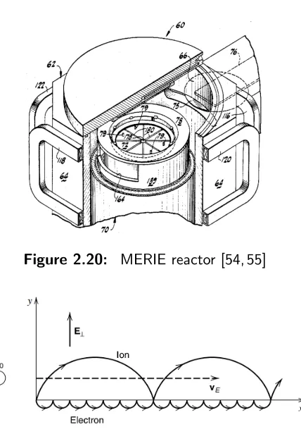
2.2.2.2 Magnetically Enhanced Reactive Ion Etching
MERIE is a special class of CCP etcher, whereby magnets are placed around
the chamber similar to a ECR reactor, here depicted by Figure 2.20. By introducing
the magnetic field parallel to the plane of the substrate the particles start to spiral as
shown in Figure 2.21.In a MERIE chamber, there are two pairs of magnets just outside
the chamber to introduce this field. The introduced field rotates clockwise between the
magnets producing a toroid of high-density plasma at the wafer surface. This increase in
plasma density helps stabilize and improve directionality and thus the anisotropy of the
reactor. It is this field addition that adds further tuning of feature profile to be possible,
Figure 2.20: MERIE reactor [54, 55]
Figure 2.21: The trajectory of electrons and ions in a constant magnetic field [34].
2.3
Spin-On Materials As an Alternative to CVD films
Many materials such as photoresist have been spin coated for a long time,
a somewhat newer technology incorporates the same principles and ideas learned from
resist to form other spin-on materials. Photoresist materials operate on simple polymer
chemistry and physics, other materials however use different mechanisms to achieve a
similar goal. In either instance, the materials have various requirements, operate on
the process of Chemical Solution Deposition (CSD) and are sensitive to many defects
when applied incorrectly. Spin coating has three stages independent of material concern,
dispense, flow dominated thinning, solvent evaporation and setting as shown in Figure
2.22. It is recommended that the wafer be spinning during the dispense step as to
better facilitate substrate wetting, this at times does require a hydrophobic or hydrophilic
Figure 2.22: The three stages of spin coating: 1:dispense, 2:flow dominated thinning, and 3:solvent evaporation and setting [56]
photoresist surface prep to change the surface from hydrophobic to hydrophilic. Following
the dispense of material provided there is good wetting, the material can start to spin out
to the desired thickness and undergoes flow dominated thinning as expressed by Figure
2.23. The ramp time for this is usually determined by the manufacturer to achieve the
appropriate crossover point at which solvent evaporation can start.It is during this thinning
step that a fair portion of the film is deposited around the edge of the substrate forming
what is known as the edge bead. Frequently an edge bead removal spin is added after
the solvent evaporation phase of deposition.
During the solvent evaporation stage the film starts to densify as a viscous
col-loidal suspension(sol), semisolid or pre-polymer solution. It is at this state that further
processing is performed to start to thermoset the material further driving off more
sol-vent. Spin defects generally arise from too low a dispense volume, too hot of a substrate,
inappropriate exhaust, inappropriate chuck material, to high a spin speed, spun material
temperature or old material. The two most common defects are comets and striations.
Comets arise from particulates in the dispensed liquid sticking to the substrate surface
and impeding flow generating an expanding cone of streaking towards the radial edge.
Striations are formed due to capillary action that becomes unbalanced due to surface
Figure 2.23: Solvent thinning following the material dispense. At the ”cross-over” point the material stops undergoing flow dominated thinning and enters the solvent evaporation
stage. [56]
SOG materials form on average from a sol-gel process. This process involves a
single-phase solution/sol that transitions from the liquid phase to the solid phase forming
a two-phase gel consisting of solid and solvent filled pores. The transition occurs via
destabilization, precipitation or supersaturation. The standard example follows the
forma-tion of silicon dioxide via the St¨ober process for hydrolyzing TEOS, to which a simplified
diagram is shown in Figure 2.25. When TEOS(Si(OC2H5)4) is dissolved in ethanol or
other organic solvent it allows it to react with water in solution. The Process follows
Figure 2.25: Sol-Gel/St¨ober Process for TEOS [57]
a couple different reactions, listed below(2.28) in order to form an oxide film. The first
two reactions 2.28a and 2.28b hydrolyze the TEOS forming a silanol product. The other
three reactions, 2.28c,2.28d and 2.28e all take the silanol product and start the process
of polymerization, where in the case of reactions 2.28c and 2.28e more water is produced
for further hydrolysis [33].
Si(OC2H5)4+H2O →Si(OC2H5)3OH +C2H5OH (2.28a)
Si(OC2H5)4+ 2H2O →Si(OC2H5)2(OH)2+ (C2H5OH)2 (2.28b)
Si(OC2H5)3OH +Si(OC2H5)4 →
(C2H5O)3Si−O−Si(OC2H5O)3+C2H5OH
(2.28d)
Si(OC2H5)3OH +Si(OC2H5)2(OH)2 →
(C2H5O)3Si−O−Si((OC2H5O)3)2OH +H2O
(2.28e)
Figure 2.26: The TEOS-ethanol-water system for sol-gel depositions [33].
Following the TEOS example, when the water to TEOS and ethanol to TEOS ratios are
equal, as shown by the dotted line in Figure 2.26, the material can then be formed into
a coat-able thin film material. Once the deposited film undergoes the final cross-linking
completing the sol-gel transition, the solvent phase (ethanol in TEOS and stage 3 in a
spin coat process) is removed, and the material is then considered a gel. Often times
the gel still contains solvent that must be removed further to completely dry the coating
forming the true microporous oxide film [33, 58]. As films progressed SOG became a
spin on dopant material as well as a planarization material by varying what the feedstock
Carbon has been used in industry as a hardmask for a while, especially at the
beginning of the start of double patterning. The first hardmasks were using a diamond-like
amorphous carbon, chosen due to its high selectivity to any number of standard CMOS
materials. [27, 29, 59–61] To call the material used diamond-like is a bit of a misnomer
as the material that was generated via a CVD process generally resided within the
ta-C:H and a-ta-C:H regions of the ternary phase diagram as depicted by Figure 2.27. As
features got smaller the a-carbon materials became too thick and changes needed to be
made [62], so carbon based spin-on materials were developed. Initially there were some
troubles producing a comparable material to the a-carbon [63, 64], namely with concerns
to wiggling [65, 66]. These problems started to go away when the fullerene material
Figure 2.27: Carbon ternary phase diagram [67, 68].
was developed [66, 69, 70]. The fullerene based material ”IM-HM-140” from Irresistible
Materials(IM) [71] used here is similar to resist in that it had a Novalac based epoxy resin
for its crosslinking material as shown in Figure 2.28b, with the fullerene based monomer
being shown in Figure 2.28a. The material developed by IM [71], is different than some
of the initial fullerene based hardmasks [69, 70] but shows good etching characteristics for
deep etching [66, 71, 72]. It has also been shown that multi-layer resist stacks perform
(a) (b)
Figure 2.28: Polymer precursors of the ”IM-HM-140” SOC material. A fullerene based monomer(Phenyl C60 Butyric Acid Methyl Ester) is shown in (a), which is also used in organic
The process flow developed at RIT was designed to closely reproduce what the
semiconductor industry uses for a SADP process module while advancing what RIT’s
current cleanroom facilities are capable of [24, 26–31]. This chapter is broken up into
two sections, the proposed process flow for a complete FinFET etch module as well as an
experiment to ensure that the films are etched with proper rate, selectivity and anisotropy.
The etching experiment is proposed such that a high degree of etch control can be achieved
with the MERIE system that RIT, which does not have an spectrophotometer for endpoint
detection. Without the proper etch data a number of critical steps, namely the etch
processes described within sections 3.1.6 and 3.1.9, would be incredibly difficult.
3.1
Process flow
The SADP process outlined here is a first step in FinFET fin formation and
is referred to in an idealized context throughout, predominantly perfect selectivity and
uniformity are assumed. This process could be expanded to quadruple patterning by
simply adding two additional layers, and will be noted when applicable for a conversion
of this process into a quadruple patterning process. All drawings are rough depictions to
worth noting that this process has a significant throughput improvement over other RIT
SADP processes in that the entirety of the process can be contained within a cluster tool
consisting of a MERIE etcher, PECVD TEOS oxide and PECVD nitride chambers [19].
3.1.1 SOC Fin Hardmask Deposition
The selection of hardmask for etching silicon generally is not particularly
impor-tant as both common oxides and nitrides are fairly selective to silicon with oxide alone
having standard ratios of 4:1 to 25:1 depending on the reference. These etch rates are
generally quoted for wet chemical etching however as opposed to dry etching [42]. A very
high selectivity is required for a high aspect ratio etch of at least 1:3 hardmask:substrate
is required. This is where carbon hardmasks have come into play and why a fullerene
derived-SOC was chosen for this layer. In addition to its selectivity toSiO2, Si3N4, and
Si. Previous work at RIT has demonstrated the SOC to be a good hardmask material
with high-aspect ratio silicon etches [21].
Silicon 80nm SOC
Figure 3.1: Deposition of the first SOC layer
3.1.2 Oxide Mandrel Deposition
The next layer to be considered is the mandrel over which the spacers are formed.
This could be chosen to be a variety of things but is most commonly either a nitride or
oxide. Here a PECVD TEOS oxide was chosen to be the mandrel material. 120nm of oxide
is the chosen thickness for this process as 100nm is the designed critical dimension, the
Silicon 80nm SOC 120nm Oxide
Figure 3.2: Deposition of what will be the mandrel layer out of PECVD TEOS oxide
3.1.3 BARC Deposition
With this process the goal is to achieve sub-lithographic features, as such a
Bottom Anti-Reflective Coating(BARC) should be deposited below the resist layer.
Pre-vious work has used a SOG over SOC in order to use the SOC as a hardmask for the
oxide etch [19, 21]. The SOG was investigated(see Section 4.1) and determined to be a
poor material for this project and with etch process improvements the SOC might not be
necessary. If the etch process is not as anisotropic with high enough selectivity, a layer of
SOC could be added prior to the BARC and very minor changes would be required. The
BARC thickness has previously been determined to be 65nm for good performance.
Silicon 80nm SOC 120nm Oxide 65nm BARC
3.1.4 Resist Coat, Expose and Develop
Photoresist is then coated onto the film stack as shown in Figure 3.4a. The
photoresist is then exposed as depicted in Figure 3.4b and developed as shown in Figure
3.4c. If the photoresist is over-exposed or over-developed a thinner resist image is what
results. Maintaining good critical dimension over the whole wafer in this regime using the
chemical development process is tricky. As such going forward a trim etch was chosen
using higher image quality from normal exposure/develop steps.
[image:52.612.129.538.266.480.2]Silicon 80nm SOC 120nm Oxide 65nm BARC 300nm Photoresist (a) Silicon 80nm SOC 120nm Oxide 65nm BARC (b) Silicon 80nm SOC 120nm Oxide 65nm BARC (c)
Figure 3.4: Photoresist coat of the film stack(a) followed by the exposure of the mandrel layer pattern(b) and the development of the Mandrel layer pattern(c)
3.1.5 BARC Open and Trim Etch
The BARC open etch is required as the BARC layer does not develop with the
resist. This is preformed with a O2 etch. Following the BARC etch/open as shown in
Figure 3.5a, the next step is to trim the pattern for the mandrel define etch that follows
as shown in Figure 3.5b. The trim etch is effectively a controlled overetch of the BARC
Silicon 80nm SOC
(a)
Silicon 80nm SOC
(b)
Figure 3.5: The BARC open etch opens up the BARC layer as shown in (a). Then the etch continues producing a trimmed feature with the trim etch as depicted in (b)
3.1.6 Mandrel Etch
This step is absolutely critical while also complicated. The primary etch gasses
for a SiO2 etch are CF4 and CHF3 . The etch needs to be as perfectly anisotropic as
possible for critical dimension definition for the sidewall spacers that come next. What
makes it complicated is that the BARC must be removed prior to the deposition of the
sidewall spacers. The BARC strip cannot be performed after the mandrel etch completes
as the SOC fin hardmask is exposed and etches in the same strip chemistry(O2 plasma).
So, what needs to be done is to stop the mandrel etch short as shown in Figure 3.6a.
The top TEOS layer should also be deposited/etched sufficiently during previous
process-ing/trimming such that it is fully removed prior to stopping the mandrel etch short. Then
as depicted by Figure 3.6b the BARC layer can be stripped allowing for the completion of
Silicon 80nm SOC
(a)
Silicon 80nm SOC
(b)
Silicon 80nm SOC
(c)
Figure 3.6: There are three steps to the mandrel etch. (a) shows the initial etch stopping short, followed by a strip of the SOC hardmask in (b) and finally completing the etch in (c)
3.1.7 PECVD Nitride Deposition
The nitride deposition for this step has a fair number of factors involved as well.
PECVD was chosen over LPCVD for a number of reasons, one simply is convenience
and efficiency; the PECVD Nitride chamber that RIT possesses is housed within the same
cluster tool that the MERIE dry etch chamber is so the wafers need only to move from one
chamber to another. In addition, PECVD takes significantly less time(minutes as opposed
to hours) as opposed to LPCVD and is likely more conformal partly based on previous
work [19]. Also, due to the SOC the process cannot use the LPCVD as the temperatures
for deposition are around800°C as opposed to PECVD which is around400°C, at around
300−400°C the SOC starts to erode at 12nm min−1. This temperature constraint for
the SOC is a primary driving force for using PECVD as opposed to LPCVD as in the
LPCVD the SOC would erode completely before the deposition would even occur. The
amount deposited should match very closely to the total height of the mandrel for the
following spacer etch step as this deposition does come to define a good portion of the
Silicon 80nm SOC
Figure 3.7: Deposition of the nitride spacer layer
3.1.8 Nitride Spacer Etch
For the spacer etch things become difficult, the nitride film when deposited at
the thickness of the mandrel has double the thickness where the spacer is to be. This
doubling of thickness allows for a bit of process variability, the etch should be performed
such that the etch is as uniform as possible under predominantly vertical etching.
Silicon 80nm SOC
Figure 3.8: Etching of the nitride spacer layer
3.1.9 Mandrel Strip
The mandrel strip step is a key point in this process as a dry etch under the
conditions within RIT’s MERIE chamber. Both the mandrel and the spacer films need
to be carefully calibrated such that selectivity is high under the chemistry(CF4 /CHF3
/C2F6 ) in the MERIE chamber. Under these chemistries the selectivity is normally 1:1 or
predominantly etches the nitride faster, despite polymer film forming thicker on nitrides
has been found but requires more research by determining an optimal etch, modifying
the material chemistry, and/or performing a pseudo-Bosch etch. The Bosch etch would
consist of a step-wise process of depositing just enough polymer for the following etch
step to only break through the oxide polymer then repeat the process, until the oxide is
stripped. This is different from a standard Bosch etch in that it involves multiple materials
as well as a anisotropic etch is performed as opposed to an isotropic etch that does not
etch where the polymer was deposited [41, 76–78].
Silicon 80nm SOC
Figure 3.9: Removal of the oxide mandrel
3.1.10 SOC etch
After the mandrel is stripped the nitride spacer can be used as a hard mask to
etch the bottom SOC in final preparation for the fin etch. It is at this point that the
nitride spacer could also be stripped, however there is little need as the nitride layer will
likely erode during the fin etch.
[image:56.612.225.424.535.622.2]Silicon
With the final pattern established the fin etch can finally be performed. SOC
was chosen to be the final hard mask as a fair amount of etch chemistry that etches
silicon will also etch nitride, so a 1:3 horizontal:vertical etch profile would be very hard
due to mask erosion. A 1:3 profile is required to adequately call the feature a fin. From
[image:57.612.224.423.240.315.2]this point, or during the etch itself, the fin can be tapered for better electrical properties.
Figure 3.11: Final fin etch into silicon substrate
3.2
Etch Rate, Anisotropy and Selectivity Study of Oxide Etching
In order to have a controllable etch that is precise there are five key components;
the etch rate, anisotropy and selectivity of the hardmask, the material to be patterned
as well as the underlying material beneath it. Uniformity is looked at after selectivity
is achieved. Without endpoint detection the mandrel etch(Section 3.1.6) and mandrel
strip(Section 3.1.9) are especially difficult. To begin to determine these response factors
a screening etch was developed as shown in Table 3.1.
RIT’s standard P5000 MERIE oxide etch recipe(B.1) has O2 as part of the
process introduced to quell polymer buildup. In this experiment O2 was not selected to
be used asO2 is more important once a it is determined how much polymer is formed and
whether or not it is excessive. The addition ofO2 also changes selectivity to carbon-based
films as O2 is the primary etchant in that material system, which provides further reason
SiO2, SiOxFy, photoresist, and SOC. BARC was not chosen as a material as in general
it has a similar rate to photoresist and since photoresist is already a film in the test it
would be redundant. The primary inputs are the three etch gases; CHF3 ,CF4 and
C2F6 , varied over five levels;0,15,30,45,and 60. Power, Pressure, Magnetic Field are held
constant throughout the test as they modify the rate and profile in more predictive ways
while not affecting the selectivity. Ar is also held constant as it provides directionality by
breaking through inhibitor formation in inhibitor-driven anisotropic ion enhanced etching,
even though it does change the partial pressures of the etches.
Through cross-sectional analysis, both vertical(Rv) and horizontal(Rh) etch
rates could be determined to show how anisotropic(A) the etch was and if the etch
would be within the acceptable tolerances for the given etch per Equation 2.17. Mask
erosion rates would be determined through Equation 2.22. For uniformity(Equations 2.24
and 2.27) the constants, α, , and δ are predominantly determined from how much the
film to be etched is uniform, erosion/how uniform the hardmask is and overetch is
accept-able/required for the process. β however will be determined through running the process
with blanket oxide over 6” wafers as the uniformity variance in the etch has more to do
Test CHF3 (SCCM) CF4 (SCCM) C2F6 (SCCM) Sample
1 0 0 45 a
2 0 30 30 b
3 0 60 60 c
4 15 15 30 d
5 15 30 15 e
6 15 45 45 f
7 30 0 60 g
8 30 30 0 h
9 30 45 15 i
10 45 0 30 j
11 45 15 0 k
12 45 60 45 m
13 60 15 60 n
14 60 45 0 p
[image:59.612.154.498.253.505.2]15 60 60 15 q
Table 3.1: Enchant selectivity test
4.1
SOG and TEOS uniformity
For various stages in the process, uniform film deposition is important either for
better coverage or for reducing the time spent overetching to clear the entire wafer. Since
PECVD Nitride was unavailable at the time of this study a focus was placed on the use
of SOG and TEOS. There were numerous issues with the SOG that RIT has, one major
issue was that the material was quite old producing comets and streaking as shown in
Figure 4.1. The streaking was caused by having too high surface tension from having too
large a percentage of TEOS to carrier solvent, ethanol, not allowing the material to flow
properly. The SOG was re-diluted in an attempt to remove the streaking but the film
was still less uniform than preferred as shown in table 4.1. With 6% non-uniformity and
a 100nm range, that is well below the acceptable tolerance for a SADP process.
With the SOG not performing well enough to process with, TEOS provided a
good alternative. It can be deposited over the hardbaked SOC for the mandrel layer. RIT’s
TEOS performed fairly well. A uniformity test was conducted over 26 wafers. Standard
processing only permits 1µm of depositions between cleans, so as such, two 5kA/500nm
depositions were performed and then a clean was run. Before all the depositions, a
as a preventive maintenance measure to not replace the bulbs as often as the tool does
not see 24/7 use. A trend was shown that the first wafer after a clean was slightly less
uniform, on the order of 0.59% or 10nm across the wafer as shown in Table 4.2 through
a 81 point scan. With a range of around 20-30nm and non-uniformity from 0.8-1.3%,
TEOS produces a viable outlet for a mandrel material over SOC for the proposed process
sections 3.1.2-3.1.6. However, a different material may be required to be developed such
as a fluorine-doped TEOS better known as Fluorinated silica glass (FSG) or a more organic
TEOS film for the mandrel removal step(process section 3.1.9) as the SOC material could
be removed if exposed to water as would be the case in a rinse tank following a Buffered
Oxide Etch (BOE) [38, 79, 80]. It can be safely assumed that proceeding with the TEOS
[image:61.612.213.433.408.536.2]as is is advised, and would produce a α value of around 0.01 for use in etch calculations.
Figure 4.1: SOG coating depicting streaks and comets
Before After
Mean(A) 8008 4419
Non-uniformity % 15 6
Range(A) 4857 1216
[image:61.612.230.419.588.654.2]Average 1st 2nd
Mean(A) 5358 5314 5401
Std dev 55 68 42
% 1 1.3 0.79
[image:62.612.229.421.71.151.2]Range(A) 247 298 195
Table 4.2: Average uniformity for 5kA depositions as well as the average data for first and second wafer through after a clean.
4.2
TEOS Etching
In order for RIT to achieve small features for a SADP process, a significant
focus needs to be placed on etching. Currently RIT has two types of etchers, CCP and
a MERIE etcher, Uniformity control on standard CCP etchers is fairly poor so this work
focused on the MERIE etcher. However the MERIE etcher was in a bit of disarray, largely,
when the tool was donated it was not given a proper cleaning prior to its use at RIT.
An effort to improve the chamber was taken prior to extensive testing. Firstly, there was
a thick, 0.5-1mm polymer film along all the sidewalls and showerhead that was cracking
and introducing particulates into the chamber. This polymer film was cleaned from the
chamber.
Following the polymer removal, it was noticed that there was a Teflon screw
cap as opposed to a polycarbonate screw cap in the showerhead as depicted in point A
of Figure 4.2. Teflon under RF conditions has a significantly different inductance than
polycarbonate, this significantly contributed to etch non-uniformities that were reported
prior to this work. The chamber was then seasoned with an Applied Materials proprietary
recipe which due to copyright cannot be replicated here. The chamber seasoning is
important as it places polymer on the sidewalls, this polymer deposition does multiple
things [81, 82]. Firstly, during any standard etch polymer is going to be deposited on
the sidewalls of the chamber, however in a unseasoned situation the etch rate for a given
A
[image:63.612.224.424.72.336.2]B
Figure 4.2: MERIE showerhead. Point (A) is where the screwcap was replaced. Point(B) roughly approximates the width of a ring formed around the showerhead pinholes that occurs
from proper seasoning.
opposed to the wafer. When the sidewalls of the chamber are passivated with polymer
then the gases tend to not interact with the sidewalls of the chamber providing more
available etchant for the wafers. Prior to cleaning the sidewall polymer with its cracking
and other non-uniformities likely provided a larger surface area for polymer to continue
to form as if the chamber had no polymer at all, that is however speculation. A rule of
thumb for seasoning RIT’s chamber was that the polymer should not be formed within
1cm of the pinholes in the showerhead as depicted by point B in Figure 4.2, this resulted in
a over-seasoned chamber and decreased rates. Following this, the clamping pressure was
adjusted and leveled. The clamp ring is depicted in Figure 4.3 in both the lifted(Figure
4.3a) and clamped(Figure 4.3b) positions, any irregular clamping pressure would produce
a left-right or right-left gradient on the wafer due to uneven helium cooling which was
![Figure 2.3:SADP simplified flow [26]](https://thumb-us.123doks.com/thumbv2/123dok_us/32528.2580/21.612.258.388.70.116/figure-sadp-simplied-ow.webp)
![Figure 2.7: Plasma reaction mechanisms [35]](https://thumb-us.123doks.com/thumbv2/123dok_us/32528.2580/24.612.108.541.72.282/figure-plasma-reaction-mechanisms.webp)
![Figure 2.11: Film growth mechanisms [36]](https://thumb-us.123doks.com/thumbv2/123dok_us/32528.2580/28.612.240.411.297.439/figure-film-growth-mechanisms.webp)
![Figure 2.12: A Gibbs energy vs Temperature curve for the formation of various oxides [36].](https://thumb-us.123doks.com/thumbv2/123dok_us/32528.2580/30.612.220.426.76.397/figure-gibbs-energy-temperature-curve-formation-various-oxides.webp)
![Figure 2.13: Normalized Gas flow lines(left) over the range of 0-1 and isotherms in K(right)for varying Reynolds and Grashof numbers for a vertical reactor design [36,37].](https://thumb-us.123doks.com/thumbv2/123dok_us/32528.2580/31.612.175.472.72.332/figure-normalized-isotherms-varying-reynolds-grashof-vertical-reactor.webp)
![Figure 2.16:Ion bombardment energy by pressure [42].](https://thumb-us.123doks.com/thumbv2/123dok_us/32528.2580/35.612.152.495.72.336/figure-ion-bombardment-energy-by-pressure.webp)
![Figure 2.17:Possible effects of RIE [51,52].](https://thumb-us.123doks.com/thumbv2/123dok_us/32528.2580/38.612.154.490.71.336/figure-possible-eects-of-rie.webp)
![Figure 2.18:Feature size specifications for etching as described by equation 2.18 [42].](https://thumb-us.123doks.com/thumbv2/123dok_us/32528.2580/39.612.205.471.357.645/figure-feature-size-specications-etching-described-equation.webp)
![Figure 2.19:Feature shrink due to mask erosion as depicted by equation 2.22 [42].](https://thumb-us.123doks.com/thumbv2/123dok_us/32528.2580/40.612.157.545.247.555/figure-feature-shrink-mask-erosion-depicted-equation.webp)