White Rose Research Online URL for this paper:
http://eprints.whiterose.ac.uk/712/
Article:
Savic, I., Milanovic, V., Ikonic, Z. et al. (3 more authors) (2004) Dilute magnetic
semiconductor quantum-well structures for magnetic field tunable far-infrared/terahertz
absorption. IEEE Journal of Quantum Electronics, 40 (11). pp. 1614-1621. ISSN
0018-9197
https://doi.org/10.1109/JQE.2004.836469
[email protected] https://eprints.whiterose.ac.uk/ Reuse
See Attached
Takedown
If you consider content in White Rose Research Online to be in breach of UK law, please notify us by
Dilute Magnetic Semiconductor Quantum-Well
Structures for Magnetic Field Tunable
Far-Infrared/Terahertz Absorption
Ivana Savic´, Vitomir Milanovic´, Zoran Ikonic´, Dragan Indjin, Vladimir Jovanovic´, and
Paul Harrison
, Senior Member, IEEE
Abstract—The design of ZnCdSe–ZnMnSe-based quantum wells is considered, in order to obtain a large shift of the peak absorption wavelength in the far infrared range, due to a giant Zeeman splitting with magnetic field, while maintaining a rea-sonably large value of peak absorption. A triple quantum-well structure with a suitable choice of parameters has been found to satisfy such requirements. A maximal tuning range between 14.6 and 34.7 meV is obtained, when the magnetic field varies from zero to 5 T, so the wavelength of the absorbed radiation decreases from 85.2 to 35.7 m with absorption up to 1.25% at low temperatures. These structures might form the basis for magnetic field tunable photodetectors and quantum cascade lasers in the terahertz range.
Index Terms—Infrared detectors, manganese alloys, magnetic field effects, quantum wells, quantum theory, tunable circuits and devices.
I. INTRODUCTION
T
HERE are a wide variety of potential applications for electronic and photonic systems operating in terahertz frequency bands (1–10 THz, 300–30 m) such as in medicine, microelectronics, agriculture, gas sensing and environmental monitoring, astronomy and satellite mapping, etc., which has driven a lot of research toward their design and fabrication. Compact coherent quantum cascade lasers and quantum-well photodetectors have been developed recently [1]–[8] which motivated new theoretical studies of terahertz physics [9]–[11]. The tunability of such terahertz sources and detectors is the next challenge for further development of terahertz photonics.Dilute magnetic semiconductors (DMS) are materials with a fraction of cations substituted by magnetic ions, e.g., Mn ions replacing some group-II cations in Zn Mn Se, Cd Mn Te, and Zn Mn Te. The magnetic properties of DMS are determined by the strong exchange interaction between the and band electrons and the [5] electrons associated with the localized magnetic ions. This
ex-Manuscript received June 23, 2004; revised July 28, 2004. This work was supported in part by the European Office of Aerospace Research and Develop-ment under Contract FA8655-04-1-3069.
I. Savic, V. Milanovic´, Z. Ikonic´, and D. Indjin are with the Institute of Microwaves and Photonics, School of Electronic and Electrical En-gineering, University of Leeds, Leeds LS2 9JT, U.K. and also with the Faculty of Electrical Engineering, University of Belgrade, Belgrade 11120, Serbia and Montenegro (e-mail: [email protected]; [email protected]; [email protected]; [email protected]).
V. Jovanovic´ and Paul Harrison are with the Institute of Microwaves and Pho-tonics, School of Electronic and Electrical Engineering, University of Leeds, Leeds LS2 9JT, U.K. (e-mail: [email protected]; [email protected]).
Digital Object Identifier 10.1109/JQE.2004.836469
change interaction affects processes which involve electrons in the conduction and valence bands, exciton and impurity levels and induces unique magneto-optical properties which are qualitatively different from those observed in nonmagnetic semiconductors [12], [13].
While interband transitions in DMS have been studied inten-sively in the last decade [12], [14], both theoretically and ex-perimentally, to our knowledge, the research of intersubband transitions has not been reported. Intersubband transitions might be of interest due to the prospect of their application in mag-netic field tunable devices. An external magmag-netic field applied to a semiconductor quantum well parallel to the confinement direction splits the in-plane continuum of quantized subbands into Landau levels, each subband producing a set of Landau levels, described by a Landau index and additionally by spin index (gyromagnetic spin splitting within Landau levels). Both the Landau level energies and their splitting depend linearly on the magnetic field.
If the structure includes DMS, the conduction band edge varies with the magnetic field locally (i.e., remains unchanged in regions comprising nonmagnetic semiconductors) and, hence, modifies the potential profile. The shift of the potential (in the magnetic layers and near the interfaces) is opposite for the two spins and, consequently, they experience two different potential profiles, which are effectively tuned by the magnetic field. This spin-dependent variation of the confinement energy is particularly significant in the vicinity of the interfaces and in turn leads to different, and field-dependent, spectra of the size-quantized component of the electron energies for the two spins, and this phenomenon is known as the giant Zeeman splitting. Since the spin and Landau level index are conserved in optical transitions caused by -polarized light, the transition energies will vary with the magnetic field, and this variation is different for the two spin states. This translates into tunability of intersubband transition energies by varying the magnetic field, in contrast to the case of nonmagnetic semiconductor-based structures where the potential profile and, hence, the size-quan-tization part of the electron energy, do not depend on the magnetic field (apart from irrelevant global shift). Due to the enhanced Zeeman splitting at an non-DMS/DMS interface and its effect on magneto-optical properties of a structure as a whole, the idealized model of DMS-based structures with abrupt interfaces is not sufficient, and an essential requirement in modeling is the inclusion of altered composition profile, which in turn modifies the spin-dependent potential profile.
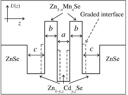
Fig. 1. A triple ZnMnSe–ZnCdSe–ZnSe quantum-well structure. Dashed lines denote 2-ML—thick intermixing regions.
The giant Zeeman splitting offers a route toward achieving magnetic field tunable absorption wavelength in DMS nanos-tructures. By increasing the magnetic field one changes the tran-sition energies and the wavelength of the absorbed radiation. For any magnetic field different wavelengths are absorbed in the spin-up and spin-down transitions within the same pair of size-quantized levels (spin-flip transitions are negligable [15]). Splittings of a few meV which are achievable in materials like ZnMnSe or CdMnTe imply a large tunability on a relative scale if the transition energy is in the terahertz range. If we com-pare quantum-well structures based upon these materials, op-erating as photodetectors, against bolometers, the latter has a very high responsivity at a few kelvin and does not require an external magnetic field. However, the magnetic field itself makes such structures frequency tunable, in contrast to either bolometers or another existing detector—the Schottky diode. The aim of this work was to engineer the structure profile of ZnSe–ZnMnSe–ZnCdSe quantum wells in respect to achieving maximum tunability of far infrared intersubband transitions by varying the magnetic field. The influence of relevant parameters (temperature, sheet density of impurities) on the absorption in the optimized structure was then examined.
II. THEORETICALMODEL
We consider a symmetric triple-coupled quantum-well structure formed from ZnSe–Zn Cd Se quantum wells separated by Zn Mn Se layers (Fig. 1). A symmetric double quantum-well structure is its special case, with . The -axis was taken to be the direction of confinement. The struc-ture was chosen to be symmetric to provide large absorption. Magnetic barrier layers were placed in the middle of the struc-ture to maximize (minimize) the influence of varying barrier heights on even (odd) parity states, which should result in maximal tunability.
The total Hamiltonian of an electron in the Zn Mn Se bar-riers is [12]–[26]
(1)
where is the conventional Hamiltonian for nonmagnetic semiconductor structures, while the - exchange contribution is contained in . Thus, reads [12]–[26]
(2)
where is the electron effective mass (here assumed constant throughout the structure, in free electron mass units, which is reasonable for low concentration of Mn and Cd), is the magnetic vector potential, is the Landé factor of conduction band electrons (here , also assumed constant), is the Bohr magneton, and is the magnetic field along the -axis. The first term of is the kinetic energy, the second term is the conduction band edge (band offset), and the third term is the potential responsible for spin splitting of Landau levels (“ ” is for spin-up and “ ” for spin-down electrons).
The – exchange potential occurs only in DMS layers, and also in interface regions due to the diffusion of Mn ions from magnetic layers, and depends on the magnetic field. Man-ganese magnetic moments contribute to the total magnetic mo-ment in the external magnetic field, forming a strong total mag-netic field which interacts with the electrons. At low Mn con-centrations they are noninteracting and all partic-ipate in the total magnetization. Besides the - interaction between the conduction band electrons and localized magnetic ions, the Mn –Mn exchange also has a significant influ-ence. The dominant nearest-neighbor exchange process is anti-ferromagnetic, reducing the number of Mn ions contributing to the total magnetic moment, and cannot be neglected at higher Mn concentrations. Therefore, an empirical expression for the spin-dependent potential induced by the magnetic field is taken [12], [18], [19]
(3)
where “ ” is for the up electrons and “ ” for the spin-down electrons, is the - exchange integral for the conduc-tion band, is the density of cations, and is the thermal average of the Mn spin, which, for paramagnetic materials amounts to
(4)
where is the Boltzmann constant, the temperature, and is the Brillouin function
(5)
Substituting these barrier potentials in the Schrödinger equa-tion, we get
(6)
in the magnetic barriers and the interface regions, and
(7)
in the nonmagnetic layers.
Using the Landau gauge the quantized state envelope wavefunctions read
(8)
where is the dimension of the structure along the -axis, is the Landau length, labels
Landau levels , and is the harmonic
oscillator wavefunction
(9)
where is the th Hermite polynomial.
Neglecting the gyromagnetic spin splitting, which is signifi-cantly smaller due to the - exchange ( 0.5 meV at T) and does not influence the transition energies, the Schrödinger equation for reads
(10)
The wavefunctions of all the Landau levels that stem from the same size-quantized electron state have the same form, the en-ergies of subsequent Landau levels being shifted by
, where is the cyclotron frequency. The electron states are specified by the set of quantum numbers , and their energies
(11)
depend on , and .
Intersubband transitions exist only in doped structures, with low-lying states occupied by electrons. In accordance with (11),
the electron sheet density and the Fermi level are related by
(12)
In optical transitions caused by -polarized light, the Landau index and spin are conserved, and absorption occurs only on transitions between different size-quantized states (hereafter refered to as the th and the th state). The fractional absorption on such a transition is [27]
(13)
(14)
where is the refraction index, and are the corre-sponding wavefunctions, with energies and for spin
, and
(15)
Transitions between states and occur only if they are of op-posite parities.
The total absorption involving one spin orientation is a sum of contributions of all Landau levels
(16)
where the spin subscript is supressed. For small magnetic fields the above sum can be replaced by Euler–Maclaurin sum-mation formula [28]
Since the integral in (17) is proportional to , in low magnetic field limit the sum can be approximated by the integral. Then the absorption takes the form
(18)
The delta function can be replaced by a Lorentzian, to account for state broadening
(19)
where is the transition linewidth (here, taken as 5 meV). The peak absorption in weak magnetic field is then given by
(20)
To address the enhanced magnetization at a non-DMS/DMS interface, a theoretical method mapping its profile in details was developed [29], [30]. It takes into account the effect of graded interfaces, the interface roughness and the enhanced magnetization at interfaces. Since the parameters used for the characterization of the interface profile are not known for ZnMnSe–ZnCdSe–ZnSe systems, we used a modified model [22], [23] that introduces a 2-monolayer-wide intermixing region left and right of the DMS barrier assuming different Mn concentrations, effective Mn concentrations and effective temperatures in the barriers and the intermixing regions. The complete potential profile of a triple quantum-well structure including the intermixing regions represented by dashed lines is shown in Fig. 1.
The band offset was calculated with the incorporation of the deformation-potential term (strain) and the variation of compo-sition profile of Mn ions in the magnetic barriers and at the inter-face using the band, strain and lattice parameters from [20]. The band offset between Zn Mn Se and ZnSe materials when they are in contact and is positive, and to a very good approximation a linear function
meV (21)
The band offset between ZnSe and Zn Cd Se is positive and in a good agreement with the following linear dependence on :
meV (22)
The difference between conduction band edges at Zn Mn Se–Zn Cd Se heterojunction is positive and can be calculated from
meV (23)
The inclusion of a modified composition profile, and spin-de-pendent potential shift in the 2-ML interface regions requires solving the Schrödinger equation in a more complicated struc-ture than a triple quantum well. This was performed by a fi-nite-difference method [31].
III. NUMERICALRESULTS ANDDISCUSSION
The design was performed by varying the thickness of the Zn Cd Se, Zn Cd Se, and Zn Mn Se layers and their composition with respect to achieving maximal tunability of the transitions between the ground and the first excited size-quan-tized states, by increasing the magnetic field from zero until the - interaction saturates which occurs at magnetic fields of 5 T. These magnetic fields are realizable by a split-pair su-perconducting coil [4]. As will be discussed later, the spin-down states experience a reduction in the barrier height and enhance-ment of the transition energies and absorption, and the parame-ters of the structure were chosen so that spin-down inparame-tersubband transitions satisfy these conditions. Another requirement was that the first excited energy state of the electrons of either spin remains at least one transition linewidth below the potential of ZnSe barriers when the - interaction saturation occurs so that the transitions of both spin electrons remain bound-to-bound and the absorption in the whole magnetic range can be calcu-lated from (20). In the case of Zn Mn Se it is [18], [19]
eV so the - potential is given by
meV (24)
As the barrier thickness decreases, interactions among the wells become stronger so the splitting becomes larger. Addition-ally, the spin splitting is increased because the antiferromagnetic interactions between magnetic ions are reduced which leads to significantly enhanced effective magnetic moments and the -potential [18], [19], [22], [23]. The thickness of magnetic bar-riers was here set to 1 nm, in the range considered in the litera-ture [18], [19]. For 1-nm-thick Zn Mn Se layers, assuming that the effective Mn concentration is and the effec-tive temperature K (same as in Zn Mn Se bulk), the effective Mn concentration and the effective temperature in the 2-ML interface regions were found to be and 1.2 K. With such magnetic barriers the maximum shift of the barrier height, and therefore of transition energies for both spin states is achieved. The maximal magnetically induced change of Zn Mn Se barrier is 41.9 meV in the intermixing regions and 12.8 meV inside the layers.
Having adopted the barrier thickness 1.12 nm (4 ML) and Mn concentration , the thickness of the inner well and the outer wells were varied, as well as the composi-tion of Zn Cd Se and Zn Cd Se materials, in order to ob-tain the radition absorption in the desired range by increasing the magnetic field until saturation occurs. The best results are obtained for 1.68 nm, 2.52 nm, , and
Fig. 2. The wavelength of the spin-up and spin-down transitions of the
designed triple ZnMnSe–ZnCdSe–ZnSe quantum-well structure (a = 1:68
nm,b = 1:12nm,c = 2:52nm,x = 0:2; y = 0:1; z = 0:25) as a function of the magnetic field for two different temperaturesT = 1:5K andT = 4:2
K whenN = 8 1 10 cm .
terms of wavelengths, the tuning range is 55.3–35.7 m for spin-down, and 55.3–95.6 m for spin-up transitions. Certainly, if the field decreases from 0 to 5 T the roles of up and spin-down transitions are interchanged. For comparison, the maximal tuning range of spin-down transition predicted in a double well structure [32] is 5.2 meV, with the structure parameters: 1.12 nm, 2.52 nm, , and . This is signifi-cantly smaller than the tuning range of the triple quantum wells. With this choice of parameters, the structure has only two size-quantized bound states. The maximal splitting of the spin-down state from the zero-field position can be made even larger with different parameters, and the magnetic field would then move the excited state up until it reaches the continuum, and only the ground state of spin-up electrons remains. Any particular Landau level and spin state con-tributes to absorption if the Fermi level is between the lower and upper state energy. This requirement is satisfied for at least one spin state for the relatively high doping sheet
den-sities cm cm , and we have taken
cm . The exact treatment would require a self-consistent solution of the Schrödinger and Poisson equations with the additional inclusion of exchange-corre-lation effects. However, previous experience [33]–[35] with self-consistent calculations of GaAlAs structures indicate that many-body effects should not significantly modify the absorption profile for cm . A more detailed analysis, incorporating many-body effects into our model, will be addressed in due course.
[image:6.594.44.287.63.242.2]The spin splitting of the Landau levels depends not only on the magnetic field and conduction band edge design, but also on temperature. From Fig. 2. one can see that the both spin transi-tion wavelengths vary with field more slowly at higher temper-atures. The same wavelength range can be achieved at higher temperatures by using stronger fields. Due to the temperature dependence of the different spin state populations, i.e., due to reduced spin polarization at higher temperatures, the - ex-change interaction decreases as the temperature increases, as
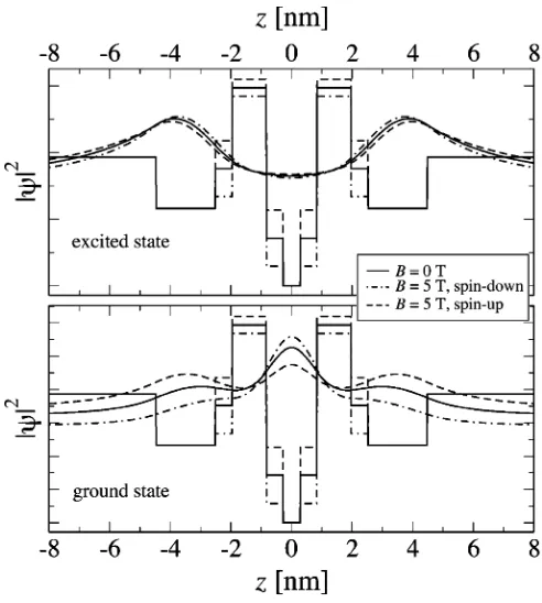
Fig. 3. The squares of the wavefunctions of the spin-degenerate electron states whenB = 0T and the spin-up and spin-down saturated states whenB = 5T in the designed triple ZnMnSe–ZnCdSe–ZnSe quantum-well structure (a = 1:68 nm,b = 1:12nm,c = 2:52nm,x = 0:2; y = 0:1; z = 0:25) whenT = 1:5
K andN = 8 1 10 cm .
well as the total spin splitting and absorption, so the magnetic field at higher temperatures has to be stronger to induce the same degree of spin polarization and splitting.
The squares of the wavefunctions corresponding to two states are shown in Fig. 3, the ground state being even and the ex-cited state odd. In the zero-field case, the major part of the even wavefunction is localized in the ZnCdSe wells, particularly in the inner one, while the odd function penetrates more into the DMS layers. The reason for the different behavior of even/odd states with increasing field clearly follows from very different overlaps of their wavefunctions with DMS or DMS interface layers, where the field variation is translated into the potential variation.
In nonmagnetic semiconductors the variation of the Landau levels is a linear function of the magnetic field. The spin splitting is rather small ( 0.5 meV at 5 T). Fig. 4(a) represents the situation assuming that the barrier material has the same prop-erties as ZnMnSe but without the - exchange included. In DMS the magnetic field induces spin-dependent changes of bar-rier heights, causing the Landau levels of spin-up (spin-down) electrons to move up (down) in energy, Fig. 4(b). The spin split-ting is inverted (the sign of the splitsplit-ting is changed) and am-plified significantly. This increases until the magnetic field be-comes strong enough that the - exchange interaction satu-rates, and beyond that point the system behaves in non-DMS manner (but with the saturated - potential profile).
Fig. 4. The fan-out of Landau levels from the two quantized states in the designed triple ZnMnSe–ZnCdSe–ZnSe quantum-well structure (a = 1:68nm,
b = 1:12nm,c = 2:52nm,x = 0:2; y = 0:1; z = 0:25) (a) assuming that thesp-dexchange interaction does not exist in ZnMnSe and (b) including the
sp-dexchange interaction in ZnMnSe as a function of the magnetic field when
T = 1:5K andN = 8 1 10 cm .
near the Fermi level, so these drops are not distinct. For stronger fields ( 2 T) the Fermi level increases, becoming close to the ground state Landau level. This Landau level increases faster than the Fermi level, causing the latter to drop, and reach the next lower Landau level. At strong enough fields there is only one Landau level near the Fermi level, so these drops are sharp and result in a staircase-like behavior of the Fermi level.
In the case shown in Fig. 4(b), for fields smaller than 2 T, at least one spin-up and one spin-down Landau levels are below the Fermi energy. Above 2 T, the spin splitting is such that all the Landau levels of the spin-up electrons are above the Fermi level. Given that the temperature is near zero, their population is extremely small, and so is the absorption on the spin-up tran-sitions. For the spin-down electrons some of the ground state Landau levels are below the Fermi level, almost completely oc-cupied and thus contributing to absorption.
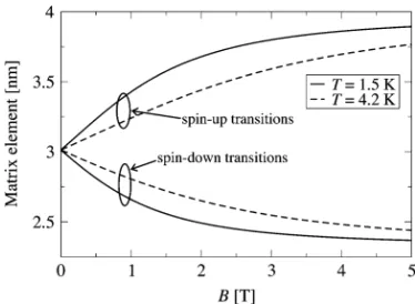
[image:7.594.332.519.64.201.2]The matrix element in the optimized structure (Fig. 5) is rela-tively large, and so is the absorption. This is due to the very thin DMS layers, which couple the ZnCdSe wells strongly enough that the wavefunction overlap is significantly better than in the structures comprising thicker DMS layers. As one can see from Fig. 3. the wavefunctions overlap for the spin-down states is smaller than in the zero-field case, and the opposite is true for spin-up states. However, the value of the absorption on spin-up or spin-down transitions results as an interplay of matrix el-ement and state population effects. Indeed, the absorption on
Fig. 5. The matrix element of the spin-down and spin-up transitions of the designed triple ZnMnSe–ZnCdSe–ZnSe quantum-well structure (a = 1:68nm,
b = 1:12nm,c = 2:52nm,x = 0:2; y = 0:1; z = 0:25) as a function of the magnetic field for two different temperaturesT = 1:5K andT = 4:2K when
[image:7.594.333.518.271.405.2]N = 8 1 10 cm .
Fig. 6. The magnetic-field-dependent absorption involving the spin-down and spin-up electrons and total absorption in the designed triple
ZnMnSe–ZnCdSe–ZnSe quantum-well structure (a = 1:68nm,b = 1:12nm,
c = 2:52nm,x = 0:2; y = 0:1; z = 0:25) for two different temperatures
T = 1:5K andT = 4:2K whenN = 8 1 10 cm .
spin-up transitions decreases from 0.65 % at zero field to zero at approximately 2 T (Fig. 6), while the absorption on spin-down transitions increases from 0.65 % to 1.25 %, reaching satura-tion before the - exchange interaction saturates. The total ab-sorption on both transitions is roughly constant across the whole magnetic field range. At zero field both contribute equally. As the field increases, the lowest spin-down Landau level popula-tion decreases and becomes negligible, and so does the corre-sponding absorption. The total electron density is determined by doping, and is independent on the field. Therefore, the number of spin-down electrons occupying the lowest levels, and the ab-sorption involving them, increase. In this paper the widths of the layers are of the order of a nanometer, which implies that inter-face roughness has a significant impact on the broadening of ab-sorption linewidth [36]. This effect was not explored in detail, or accounted for in our calculations of the peak absorption. In-cluding this broadening would scale the results, but the general shape of the absorption profile would be preserved. The contri-bution of interface roughness scattering to absorption linewidth will be considered in future work.
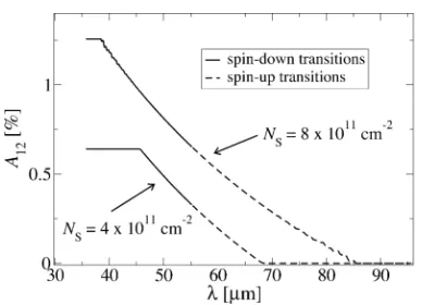
Fig. 7. The absorption involving the spin-down and spin-up electrons in the designed triple ZnMnSe–ZnCdSe–ZnSe quantum-well structure (a = 1:68nm,
b = 1:12nm,c = 2:52nm,x = 0:2; y = 0:1; z = 0:25) as a function of the wavelength for two different impurity sheet densitiesN = 8 1 10 cm and
N = 4 1 10 cm whenT = 1:5K.
that this effect occurs only at weaker fields (1–2 T). In this range the drops are not prominent, and plateaus rather than drops and spikes are observed (the inset of Fig. 6). The effect diminishes as the temperature increases. At stronger fields only the spin-down transitions occur, as noted above, and the drops will not affect the absorption.
The influence of temperature on absorption is qualitatively similar to its influence on the absorbtion wavelength. For a fixed field the spin-down transitions are weaker at higher tempera-tures, and the spin-up transitions become stronger. If the mag-netic field is very strong the absorption becomes almost inde-pendent of temperature, Fig. 6. This is because a larger field has to be used to increase spin polarization at higher temperatures in order to achieve splitting appropriate to a particular wavelength. Another interesting effect to note is that the practically achiev-able tuning range may be reduced by inappropriate doping. For instance, with the doping density of cm the absorption is zero in the wavelength range (85.2–95.6 m), and this part of the theoretically possible tuning range (35.7– 95.6 m) is cut off (Fig. 7). At lower doping densities an even wider range of wavelengths would be cutoff.
A good external tunability of the designed structure is pre-dicted. However, in any real terahertz intersubband laser or pho-todetector device design other wavelength-dependent character-istics should be considered. For example, free carrier losses de-pend on working wavelengths, hence, waveguide structure opti-mization [1] will be necessary. Also, photodetector background limited infrared performance is influenced by peak detection wavelength and doping density and injector barrier thickness optimization will be required [7].
IV. CONCLUSION
Intersubband absorption in a magnetic-field tunable triple quantum-well structure, which includes dilute magnetic semi-conductor layers, was investigated. The magnetically induced spin splitting is found to enable tuning of the absorption wavelength. The structure parameters were engineered to get maximal tunability in the desired range of the far infrared spectrum, and the influence of magnetic field, temperature and doping on the energy spectrum and absorption was explored.
REFERENCES
[1] R. Köhler, A. Tredicucci, F. Beltram, H. E. Beere, E. H. Linfield, A. G. Davies, D. A. Ritchie, R. C. Iotti, and F. Rossi, “Terahertz semicon-ductor-heterostructure laser,”Nature, vol. 417, pp. 156–159, 2002. [2] M. Rochat, L. Ajili, H. Willenberg, J. Faist, H. E. Beere, A. G. Davies,
E. H. Linfield, and D. A. Ritchie, “Low-threshold terahertz quantum cascade lasers,”Appl. Phys. Lett., vol. 81, pp. 1381–1383, 2002. [3] B. S. Williams, H. Callebaut, S. Kumar, Q. Hu, and J. Reno, “3.4-THz
quantum cascade laser based on longitudinal-optical-phonon scattering for depopulation,”Appl. Phys. Lett., vol. 82, pp. 1015–1017, 2002. [4] J. Alton, S. Barbieri, J. Fowler, H. E. Beere, J. Muscat, E. Linfield, D.
A. Ritchie, G. Davies, R. Köhler, and A. Tredicucci, “Magnetic field in-plane quantization and tuning of population inversion in a THz su-perlattice quantum cascade laser,”Phys. Rev. B, vol. 68, p. 081 303 (R), 2003.
[5] P. Harrison and R. A. Soref, “Population-inversion and gain estimates for a semiconductor TASER,”IEEE J. Quantum Electron., vol. 37, pp. 153–157, Jan. 2001.
[6] M. Graf, G. Scalari, D. Hofstetter, J. Faist, H. Beere, E. Linfield, D. Ritchie, and G. Davies, “Terahertz range quantum well infrared pho-todetector,”Appl. Phys. Lett., vol. 84, pp. 475–477, 2004.
[7] H. C. Liu, C. Y. Song, A. J. SpringThorpe, and J. C. Cao, “Terahertz quantum-well photodetector,”Appl. Phys. Lett., vol. 84, pp. 4068–4070, 2004.
[8] N. E. I. Etteh and P. Harrison, “Carrier scattering approach to the origins of dark current in mid- and far-infrared (terahertz) quantum-well inter-subband photodetectors (QWIPs),”IEEE J. Quantum Electron., vol. 37, pp. 672–675, May 2001.
[9] J. C. Cao, “Interband impact ionization and nonlinear absorption of tera-hertz radiation in semiconductor heterostructures,”Phys. Rev. Lett., vol. 91, p. 237401, 2003.
[10] C. Zhang, “Dynamic screening and collective excitation of an electron gas under intense terahertz radiation,”Phys. Rev. B, vol. 65, p. 107153, 2002.
[11] J. C. Cao, H. C. Liu, X. L. Lei, and A. G. U. Pereira, “Chaotic dynamics in terahertz-driven semiconductors with negative effective mass,”Phys. Rev. B, vol. 63, p. 115308, 2001.
[12] J. K. Furdyna, “Diluted magnetic semiconductors,”J. Appl. Phys., vol. 64, pp. R29–R63, 1988.
[13] J. A. Gaj, Diluted Magnetic Semiconductors, J. K. Furdyna and J. Kossut, Eds. Boston, MA: Academic, 1988, vol. 25, ch. 7.
[14] J. K. Furdyna, J. Kossut, and A. K. Ramdas, Optical Properties of Narrow-Gap Low-Dimensional Structures, C. M. S. Torres, J. C. Portal, J. C. Maan, and R. A. Stradling, Eds. New York: Plenum, 1987, p. 135.
[15] G. Bastard and R. Ferreira, “Spin-flip scattering times in semiconductor quantum wells,”Surf. Sci., vol. 267, pp. 335–341, 1992.
[16] N. Malkova and U. Ekenberg, “Spin properties of quantum wells with magnetic barriers. I. Ak 1 panalysis for structures with normal band ordering,”Phys. Rev. B, vol. 66, p. 155 324, 2002.
[17] S. P. Hong, K. S. Yi, and J. J. Quinn, “Self-consistent electronic structure of spin-polarized dilute magnetic semiconductor quantum wells,”Phys. Rev. B, vol. 61, pp. 13745–13751, 2000.
[18] S. Lee, M. Dobrowolska, J. K. Furdyna, H. Luo, and L. R. Ram-Mohan, “Magneto-optical study of interwell coupling in double quantum wells using diluted magnetic semiconductors,”Phys. Rev. B, vol. 54, pp. 16939–16951, 1996.
[19] S. Lee, M. Dobrowolska, J. K. Furdyna, and L. R. Ram-Mohan, “En-hancement of Zeeman splitting in double quantum wells containing ul-trathin magnetic semiconductor layers,”Physica E, vol. 10, pp. 300–304, 2001.
[20] P. J. Klar, D. Wolverson, J. J. Davies, W. Heimbrodt, and M. Happ, “De-termination of the chemical valence-band offset for Zn Mn Se/ZnSe multiple-quantum-well structures of highx,”Phys. Rev. B, vol. 57, pp. 7103–7113, 1998.
[21] P. M. Young, H. Ehrenreich, P. M. Hui, and K. C. Hass, “Electronic structure of superlattices incorporating diluted magnetic semiconduc-tors,”Phys. Rev. B, vol. 43, pp. 2305–2314, 1991.
[22] J. M. Fatah, T. Piorek, P. Harrison, T. Stirner, and W. E. Hagston, “Nu-merical simulation of antiferromagnetic spin-pairing effects in diluted magnetic semiconductors and enhanced paramagnetism at interfaces,”
Phys. Rev. B, vol. 49, pp. 10341–10344, 1994.
[24] K. Chang, J. B. Xia, and F. M. Peeters, “Longitudinal spin transport in diluted magnetic semiconductor superlattices: The effect of the giant Zeeman splitting,”Phys. Rev. B, vol. 65, pp. 155–211, 2002.
[25] N. Kim, S. J. Lee, T. W. Kang, K. S. Yi, and G. Ihm, “Magnetization of a ferromagnetic diluted magnetic quantum well in a parallel magnetic field,”J. Kor. Phys. Soc., vol. 39, pp. 1050–1054, 2001.
[26] T. Jungwirth, W. A. Atkinson, B. H. Lee, and A. H. MacDonald, “In-terlayer coupling in ferromagnetic semiconductor superlattices,”Phys. Rev. B, vol. 59, pp. 9818–9821, 1999.
[27] S. ˘Zivanovic´, V. Milanovic´, and Z. Ikonic´, “Intraband absorption in semiconductor quantum wells in the presence of a perpendicular magnetic field,”Phys. Rev. B, vol. 52, pp. 8305–8311, 1995.
[28] Handbook of Mathematical Functions with Formulas, Graphs, and Mathematical Tables, M. Abramowitz and I. A. Stegun, Eds., Dover, New York, 1965, p. 16.
[29] J. A. Gaj, W. Grieshaber, C. Bodin-Deshayes, J. Cibert, G. Feuillet, Y. Merle d’Aubigne, and A. Wasiela, “Magneto-optical study of inter-face mixing in the CdTe-(Cd, Mn)Te system,”Phys. Rev. B, vol. 50, pp. 5512–5527, 1994.
[30] W. Grieshaber, A. Haury, J. Cibert, Y. Merle d’Aubigne, A. Wasiela, and J. A. Gaj, “Magneto-optical study of the interface in semimagnetic semiconductor heterostuctures: Intristic effect and interface profile in CdTe-Cd Mn Te,”Phys. Rev. B, vol. 53, pp. 4891–4904, 1996. [31] V. Jovanovic´, Z. Ikonic´, D. Indjin, P. Harrison, V. Milanovic´, and R.
A. Soref, “Designing strain-balanced GaN/AlGaN quantum well struc-tures: Application to intersubband devices at 1.3 and 1.55m wave-lengths,”J. Appl. Phys., vol. 93, pp. 3194–3197, 2003.
[32] I. Savic´, V. Milanovic´, Z. Ikonic´, D. Indjin, V. Jovanovic´, and P. Harrison, “Diluted magnetic semiconductor based quantum wells for field-tunable absorption in the THz range,” inCMMP Conf. 2003. Abs. Book, Paper SEO.P.2.6.
[33] J. Radovanovic´, V. Milanovic´, Z. Ikonic´, D. Indjin, V. Jovanovic´, and P. Harrison, “Optimal design of GaN–AlGaN Bragg-confined struc-tures for intersubband absorption in the near-infrared range,”IEEE J. Quantum Electron., vol. 39, pp. 1297–1304, 2003.
[34] B. Mitrovic´, V. Milanovic´, and Z. Ikonic´, “Semiconductor quantum-wells with inplane magnetic-field—The self-consistent treatment,”
Semiconduc. Sci. Technol., vol. 6, pp. 93–97, 1991.
[35] Z. Ikonic´, V. Milanovic´, and D. Tjapkin, “Resonant 2nd harmonic-gener-ation by a semiconductor well in electric-field,”IEEE J. Quantum Elec-tron., vol. 25, pp. 54–60, Jan. 1989.
[36] T. Unuma, M. Joshita, T. Noda, H. Sakaki, and H. Akiyama, “Intersub-band absorption linewidth in GaAs quantum wells due to scattering by interface roughness, alloy disorder, and impurities,”J. Appl. Phys., vol. 93, pp. 1586–1597, 2003.
Ivana Savic´was born in Poz´ega, Yugoslavia, in 1979. She recieved the B.Sc. degree in electrical engineering from the University of Belgrade, Belgrade, Yu-goslavia (now Serbia and Montenegro), in 2003. She is currently pursuing the Ph.D. degree at the Institute of Microwaves and Photonics, School of Electronic and Electrical Engineering, University of Leeds, Leeds, U.K., in the field of di-lute magnetic semiconductors-based terahertz intersubband devices.
Vitomir Milanovic´was born in Svetozarevo, Yugoslavia, in 1947. He received the B.Sc, M.Sc, and Ph.D. degrees in electrical engineering from the University of Belgrade, Belgrade, Belgrade, Yugoslavia (now Serbia and Montenegro), in 1971, 1977, and 1983, respectively.
He is currently a Full Professor at the Faculty of Electrical Engineering, Uni-versity of Belgrade. His research interests include the electronic stucture and optical properties of quantum wells and superlattices.
Zoran Ikonic´was born in 1956 in Belgrade, Yugoslavia. He received the B.Sc., M.Sc., and Ph.D. degrees in electrical engineering from the University of Bel-grade, BelBel-grade, Yugoslavia (now Serbia and Montenegro), in 1980, 1984, and 1987, respectively.
Since 1981 he has been with the Faculty of Electrical Engineering, Univer-sity of Belgrade (Full Professor from 1998). In 1999 he joined the Institute of Microwaves and Photonics, University of Leeds, Leeds, U.K. His research in-terests include the electronic structure, optical and transport properties of semi-conductor nanostructures, and devices based upon them.
Dragan Indjinwas born in Zemun, Yugoslavia, in 1963. He received the B.Sc., M.Sc., and Ph.D. degrees in electrical engineering from the University of Bel-grade, Yugoslavia (now Serbia and Montenegro), in 1988, 1993, and 1996, re-spectively.
He currently holds the position of Associate Professor at the Faculty of Elec-trical Engineering, University of Belgrade. In 2001, he joined the Institute of Microwaves and Photonics, University of Leeds, Leeds, U.K. His research inter-ests include the electronic structure, optical and transport properties of quantum wells, superlattices ,and quantum cascade structures from near- to far-infrared spectral range.
Vladimir Jovanovic´was born in Belgrade, Yugoslavia, in 1978. He recieved the B.Sc. degree in electrical engineering from the University of Belgrade, Bel-grade, Yugoslavia (now Serbia and Montenegro), in 2002. He is currently pur-suing the Ph.D. degree at the Institute of Microwaves and Photonics, School of Electronic and Electrical Engineering, University of Leeds, Leeds, U.K., in the field of GaN-based near-infrared and terahertz intersubband devices.
Paul Harrison(SM’99) received the B.Sc. degree from the University of Hull, Hull, U.K., in 1988, and the Ph.D. degree from the University of Newcastle-upon-Tyne, Newcastle-Newcastle-upon-Tyne, U.K., in 1991.