A STUDY OF THE ELECTRICAL
PROPERTIES OF POLYCRYSTALLINE BASED
ORGANIC DEVICES
Thesis submitted in accordance with the requirements
of the University of Liverpool for the degree of Doctor
in Philosophy
by
SIDRA AFZAL
iii
ABSTRACT
A study of the Electrical Properties of Polycrystalline based Organic
Devices
Sidra Afzal
In this thesis, examination of polycrystalline organic based devices such as the Schottky diode and MOS capacitor is carried out. The data is interpreted in terms of a polycrystalline model based mainly on a conventional polysilicon model with slight modifications to fit the organic properties. A brief introduction to the existing charge transport models for organic materials is presented. The most dominant being the variable range hopping model for disordered materials. The disorder analysis is appropriate in the grain boundaries of a polycrystalline material. The distribution of the traps of density of states (DOS) is commonly described by the Gaussian distribution and the associated exponential approximate at low energies. This is a valid assumption for organic semiconductors with low carrier mobility values [N. Sedghi et al., J. Non Crys. Solids 352, 1641, 2006].
iv
temperature of the states (TC) decrease. Similar analysis is carried out on doped layers of TIPS with a different insulating binder Poly-alpha methylstyrene (PAMS). The value of Wdep, LDe, T0, μeff, ND/p, MNE and TC obtained from such doped Schottky diode are approximately 100 nm, 5 nm, 1200 K, 1x10⁻² cm2V-1s
-1
, 2x1017 cm-3, 35 meV and 400 K, respectively. The Capacitance-Voltage (C-V) analysis on polycrystalline Schottky diodes provides ND of approximately 7.6 x 1016 cm-3, 5.2 x 1014 cm-3 and 2.98 x 1014cm-3 at 500 Hz, 1 kHz and 2 kHz respectively. These ND values are lower than those extracted from current-voltage characteristics and decrease with increasing frequency. This is thought to be due to the low mobility of holes, unable to respond to the signal at higher frequencies.
The conduction in polycrystalline organic Schottky diode is proposed using a 2-dimensional (2D) model, which focuses on both the lateral and vertical conduction paths. The organic semiconductor layer is assumed to be relatively thin so that only a single layer of the grain exists between adjacent grain boundaries for the vertical conduction. A two dimensional situation is treated as two separate one dimensional problems that are positioned at right angles to each other. The grain and grain boundaries in the polycrystalline material are explained in terms of two boundary conditions. The variation of potential in grain boundary is the basis in defining the variation of potential in the grains. Conduction under forward bias in the grain and grain boundary is thus established assuming two distributions for the DOS, namely the Gaussian and Laplace. In comparison, Laplace DOS is believed to be a better representation of the distribution of states, where a large number of energy levels are being scanned with applied voltage.
v
13 kΩ, 760 pF and less than 309 Ω respectively, for an organic film thickness (tOSC) of 27nm. For ND ≈ 3.6 x 1017cm-3 at 1 kHz, the hole mobility is found to be approximately 4.6x10⁻⁷cm2V-1s-1. As expected the mobility decreases with increase in frequency. Furthermore, the temperature study of inverse square space charge capacitance (1/CS
2
vi
CONTENTS
ABSTRACT ... III
CONTENTS ... VI
ACKNOWLEDGEMENTS ... XI
ABBREVIATIONS ... XII
SYMBOLS ... XIII
CHAPTER 1- INTRODUCTION ... 1
1.1 INTRODUCTION TO ORGANIC MATERIALS AND TECHNOLOGY ... 2
1.2 THESIS ORGANISATION ... 4
1.3 CONTRIBUTIONS ... 6
1.4 REFERENCES ... 8
CHAPTER 2- CHARGE TRANSPORT MECHANISMS IN ORGANIC MATERIALS ... 9
2.1 INTRODUCTION ... 10
2.2 ORGANIC MATERIALS ... 10
2.2.1 Disordered Organic Semiconductor ... 11
2.2.2 Polycrystalline Organic Semiconductor ... 12
2.3 DISTRIBUTION FUNCTIONS FOR OCCUPANCY OF THE CARRIERS .. 13
2.4 MODELS FOR DENSITY OF STATES (DOS)... 15
2.4.1 Gaussian Distribution ... 15
2.4.2Exponential Distribution of States ... 16
2.4.3 Laplace Distribution ... 18
2.4.4 Significance of Meyer Neldel Energy in DOS ... 19
2.5 CHARGE TRANSPORT MECHANISMS IN ORGANICS ... 21
vii
2.5.2 Percolation Model ... 24
2.5.3 Polaron Model ... 26
2.5.4 Variable Range Hopping Model ... 28
2.5.5 Multiple Trap and Release Model ... 30
2.5.6 Charge Transport in Polycrystalline Organic Semiconductors ... 31
2.6 SUMMARY ... 36
2.7 REFERENCES ... 37
CHAPTER 3- ANALYSIS OF POLYCRYSTALLINE ORGANIC SCHOTTKY DIODES...41
3.1 INTRODUCTION ... 42
3.2 FUNDAMENTAL THEORY OF SCHOTTKY DIODES ... 43
3.2.1 Contact Barrier Height in Ordered Inorganic Semiconductors... 43
3.2.2 Schottky Effect ... 46
3.3 TIPS-PENTACENE BASED SCHOTTKY DIODES ... 50
3.3.1 Fabrication of TIPS-Pentacene Schottky Diodes... 50
3.3.2 Electrical Characteristics of TIPS-Pentacene Schottky ... 54
3.4 TEMPERATURE EFFECTS ON THE ELECTRICAL CHARACTERISTICS OF TIPS-PENTACENE SCHOTTKY DIODES ... 75
3.4.1 Experimental Details ... 75
3.4.2 Temperature Effects on TIPS/PTAA Schottky Diode ... 76
3.4.3 Temperature Effects on Doped TIPS/PAMS Schottky Diode ... 86
3.5 CAPACITANCE-VOLTAGE (C-V) CHARACTERISTICS OF TIPS-PENTACENE SCHOTTKY DIODE ... 99
3.7 DISCUSSION AND CONCLUSION ... 102
3.8 REFERENCES ... 105
CHAPTER 4- TWO DIMENSIONAL MODEL FOR ORGANIC POLYCRYSTALLINE SEMICONDUCTOR MATERIALS ... 110
4.1 CHARGE TRANSPORT IN POLYCRYSTALLINE ORGANIC MATERIALS ... 111
4.2 CHARGE TRANSPORT IN LATERAL PATH... 112
4.3 POTENTIAL VARIATION IN GRAINS AND GRAIN BOUNDARIES ... 118
viii
4.4 CONDUCTION UNDER FORWARD BIAS ... 130
4.4.1 Assuming Gaussian DOS ... 130
4.4.2 Assuming Laplace DOS ... 132
4.5 CONCLUSION ... 136
4.6 REFERENCES ... 137
CHAPTER 5- ANALYSIS OF POLYCRYSTALLINE ORGANIC METAL-OXIDE-SEMICONDUCTOR (MOS) CAPACITORS ... 139
5.1 INTRODUCTION ... 140
5.2 CONVENTIONAL MOS CAPACITORS ... 141
5.2.1 Accumulation Region ... 141
5.2.2 Flat Band Condition ... 144
5.2.3 Depletion Region ... 145
5.2.4 Inversion Region ... 148
5.3 FABRICATION OF POLYCRYSTALLINE ORGANIC MOS CAPACITORS ... 150
5.4 CAPACITANCE VOLTAGE CHARACTERISTICS ... 153
5.4.1 Effects of Oxide and Interface charge on C-V Characteristics ... 158
5.4.2 Effect of Air Exposure ... 160
5.5 CAPACITANCE-VOLTAGE FREQUENCY CHARACTERISTICS ... 162
5.5.1 Small Signal Behaviour of an Ideal Organic MOS Capacitor ... 166
5.6 CAPACITANCE-VOLTAGE TEMPERATURE CHARACTER-ISTICS ... 174
5.6.1 Experimental Procedure ... 174
5.6.2 Effects of Temperature Variance ... 174
5.7 CONCLUSION ... 183
5.8 REFERENCES ... 185
CHAPTER 6- CONCLUSION AND FURTHER RESEARCH PROSPECTS ... 189
6.1 DISCUSSION AND CONCLUSION ... 190
6.2 FURTHER RESEARCH PROSPECTS ... 197
ix
APPENDICES ... 203
APPENDIX A: Carrier concentration in an n-type and a p-type semiconductor ... 204
Carrier concentration in an n-type semiconductor ... 204
Carrier concentration in a p-type semiconductor ... 205
APPENDIX B: Space charge limited currents (SCLC) in saturation in terms of universal mobility law (UML) ... 206
APPENDIX C: Current continuity equation ... 208
APPENDIX D: First boundary condition ... 211
APPENDIX E: Defining the curve in grains... 213
APPENDIX F: Second boundary condition in grain... 214
APPENDIX G: Total intrinsic concentration in a disordered material ... 215
APPENDIX H: Relationship of capacitance and temperature in disordered grain boundaries... 216
APPENDIX I: 1/CS2 variation with temperature in ordered grains ... 218
APPENDIX J: Conferences and journal papers ... 219
Journal Papers ... 219
x
Dedicated
to
xi
ACKNOWLEDGEMENTS
I am eternally grateful to almighty Allah (s.w.t) for giving me all that I have ever asked for. Without His wish I would not be close to where I am now and wish to be. I am eternally thankful.
I wish to express my sincere appreciation to my supervisors, Dr. M. Raja and Professor W. Eccleston for their continuous guidance, knowledgeable conversations and time throughout my research. I would like to show gratitude to Dr. D. Donaghy and Dr. R. Myers for their educated discussions, assistance in the clean rooms and willingness to help. I am a part of a truly wonderful group. I would also like to thank the European Commission through Fp6 ‘PolyNet’ project and Northwest Development Agency through ‘Northern Way’ project for their financial support.
My greatest recognition extends towards my parents for without their full confidence, support, guidance, prayers and immense love, I would not have been able to succeed. I also extend my special thanks to my caring sister, Mehak, for always being there to help me and uplift my mood. I am thankful for their presence even though they are so far away. I love them all forever dearly. Moreover, significant credit goes to my husband, Shiraz, for his continuous encouragement, support, thoughtfulness and love throughout my degrees. His constant dedication towards me has been my motivation through the hardest of my times. In addition, I am forever grateful to my grandma, Aunt Ruby, Uncle Liaqat and my cousins for their regular prayers and immense affection. Furthermore, I am highly appreciative of my new family for tolerating my absence and continuously supporting me in my studies and other activities.
xii
ABBREVIATIONS
DDQ 2, 3-Dichloro-5, 6-dicyano-1, 4-benzoquinone
DOS Density of states
HOMO Highest occupied molecular orbital
L1 Laplace first distribution law
LUMO Lowest unoccupied molecular orbital
MNE Meyer Neldel Energy
MOS Metal- Oxide- Semiconductor
MTR Multiple trap and release
OFET Organic field effect transistors OLED Organic light emitting diode OTFT Organic Thin film transistors
P3HT Poly3-hexylthiophene
PTAA Polytriarylamine
RFID Radio frequency Identification Tags
SAM Self aligned monolayer
SCLC Space charge limited currents
TIPS-pentacene 6, 13-triisopropylsilyethynyl pentacene
UML Universal mobility law
xiii
SYMBOLS
Absolute Temperature
Acceptor ion
concentration Activation energy
ν0 Attempt-to-hop frequency
k Boltzmann’s Constant qVbi Built- in potential
Bulk admittance Bulk Capacitance Bulk Resistance
Capacitance of the
Depletion Region
n(E) Carrier concentration at energy level E
Carrier concentration at Fermi level
Carrier concentration at the surface
Carrier concentration in
semiconductor bulk
T0 Characteristic
temperature describing the width of the carrier distribution
Characteristic
temperature of density
of states (DOS)
Charge in depletion
region
Concentration of trapped charge
Conductivity Contact resistance
J Current Density Debye Length
N(0) Density of states per unit volume at the Fermi level
Density of states that
can be part of the percolating sub-network
Depletion Region
Width
Dielectric constant of the insulator
Dielectric constant of
the oxide (~10 for Al2O3)
Dielectric constant of
the semiconductor
xiv
Dij Distance between two hopping states
λ Distribution width of Laplace distribution function/ Gaussian distribution function Drift mobility
Effective Debye Length Effective mobility
F Electic field
Electric Field across the
oxide layer
Electric Field at the oxide-semiconductor interface
Electric Potential (V)
q Electron affinity
EC Energy at Conduction band
Energy at Intrinsic Level
Evac Energy at vacuum level
EV Energy at Valence band
Eg Energy band gap
E ‘ Energy barrier
Et Energy of the trap states
m Exponent dependent on and the material
EF Fermi Level Energy
Fixed oxide charge Flat-band Capacitance
Vfb Flat-band voltage
Flux Force
Fraction of localized states occupied by the carrier
δ Fraction of states occupied
Free carrier
concentration
High-frequency
permittivity of the semiconductor
Interface charge
Interface trap charges Er Intra-molecular
reorganization energy Intrinsic carrier concentration
Inverse localization length
Maximum Capacitance
Maximum Depletion
Region Width
Maximum distance
xv states
Maximum energy that
any initial or final state can have.
Minimum Capacitance Minimum potential at
grain centre
Mobile ion content
, K Mobility prefactor
Oxide Capacitance Oxide trapped charges
Permittivity of free space
Permittivity of free space
Potential at full grain curve
Potential at the edge of the grain
α Ratio between the
effective density of states at the transport band edge and the density of trap
b Size of the localized states
The ratio of free carrier concentration to the
total carrier
concentration
Thickness of the
organic semiconductor
Thickness of the oxide
layer
VT Threshold Voltage
Time taken for a hop to take place
Total admittance Total Capacitance Total impedance
Total MOS capacitance
Total Resistance
Transport energy in a
disordered material Transport energy in an crystalline material
2 2 Variance of Laplace distribution function
VG Voltage applied at the
gate contact
Work function
difference between the
metal and the
semiconductor
Work function of the Metal
Work function of the
CHAPTER 1- INTRODUCTION
1.1 INTRODUCTION TO ORGANIC MATERIALS AND TECHNOLOGY
Considerable research and effort is undertaken to understand semiconducting, conducting and light emitting properties of the organic materials for the improvement of organic electronics. This is done so by the use of different synthesis and self-assembly techniques. Unique opportunities exist for the improvements in the performance of these organic materials for the use in large area, low temperature devices made on substrates such as a paper or plastic. These materials are capable of generating new applications for the use in technologies as computing and connectivity devices.
The possibility to optimise the properties of the organic materials by synthetic chemists has provided much success and development in the organic electronics industry. Research work throughout the past four decades has led to a dramatic improvement in the performance by the use of innovative chemistry, processing, ability to grow, control over the self assembly and subsequently the ordering of the material. Development of materials such as longer-chain conjugated polymers, organic–inorganic composites, conjugated organic small molecules, and short-chain oligomers is under progress. These materials possess the ability to emit light, conduct current, and act as semiconductors. Their conducting and semiconducting properties are present due to the ability to transport charge by the overlap of p-orbital between neighbouring molecules. The organic materials can be made to self-assemble in order to improve the p-orbital overlap, consequently improving the carrier mobility. Some of these materials also possess the ability to be flexible and tough such that they can be used in processes at low temperatures with techniques such as solution casting, vacuum evaporation, stamping and ink-jet printing. New products can thus be produced using methods such as roll to roll manufacturing. Products include radio frequency identification (RFID) tags, logic for smart cards and low cost information displays on flexible plastic materials.
organic p-type pentacene has shown mobilities of ~3 orders of magnitude lower than single crystal silicon [4].
Table 1.1. Comparison between mobility values of various organic materials and Silicon.
Semiconductor
Mobility (cm
2V
-1s
-1)
Silicon Single crystal 300-900
Polycrystalline 50-100
Amorphous ~1
P3HT < 2 x 10⁻¹ [5, 6]
PTAA 4 x 10⁻² - 4 x 10⁻³ [7]
Pentacene ~1
TIPS-pentacene ~1.2 [8]
The performance and commercialization of organic semiconductors used as inorganic materials have already been reported in literature. However, there are still a number of challenges posed by organic semiconductors. To compete with the existing standards and keep a strong market presence, organic semiconductors must perform better than the inorganic ones. New organic manufacturing processes must be cost effective offering electrical devices that are not only cheaper than inorganic devices but novel at the same time. Moreover, semiconductor lifetimes and charge transport properties are affected by surroundings such as air and water. Change in the chemical structure of semiconductor and hence the electrical properties are observed with time resulting in a decline in performance [9]. Thus a reliable method to improve semiconductor lifetime for organic devices such as optoelectronics devices is by encapsulation so that air and water have a no or limited effect on the device performance [10].
1.2 THESIS ORGANISATION
The aim of this thesis is to present an insight into the electrical properties of organic polycrystalline semiconductors, with ultimate interest in developing models for organic semiconductor devices. Fabrication and measurements of fundamental devices such as the Schottky diode and MOS capacitor are presented in detail. The data obtained is interpreted in terms of a polycrystalline model based on existing conventional poly-silicon and disordered models. Electrical characteristics of the Schottky diode and small signal analysis of MOS capacitors provide vital information for modelling. Furthermore, an attempt is made on modelling polycrystalline organic Schottky diode under forward bias. It is believed that simple models for organic devices can eventually be incorporated together for the modelling of both dc and ac organic circuits.The section below briefly introduces the chapters in this thesis.
The charge transport in crystalline inorganic semiconductors is through well ordered energy levels that overlap to form energy bands. The resulting valence and the conduction bands are for electron and hole transport. The electrons can exist in s-, p-, d- and f- orbitals. However, the atoms in a typical organic system have their electrons in the s- and p- orbital which form molecules with σ- and π- bonds respectively. The overlapping of two π- π bonds in between the molecules and other bonds such as the van der Waal bonds causes the formation of two different energy bands namely the Highest Occupied Molecular Orbital (HOMO) and the Lowest Unoccupied Molecular Orbital (LUMO) band. These are akin to the valence and conduction bands in inorganic semiconductor respectively.
Carrier conduction is possible with the application of an externally applied voltage in the organic material, just as in inorganic materials. Externally applied bias causes injection of holes into the HOMO level or electrons in the LUMO band, and subsequently the organic material behaves either as a p-type or an n- semiconductor. Nevertheless, subtle differences exist between organic and inorganic materials that must be analysed with caution.
distribution which can be likely approximated to an exponential distribution for the density of states (DOS) in the band tail. The Meyer Neldel Energy (MNE), related to the width of the Gaussian distribution or the slope of the exponential can be consequently defined. This is also attributed to disorder nature in the material.
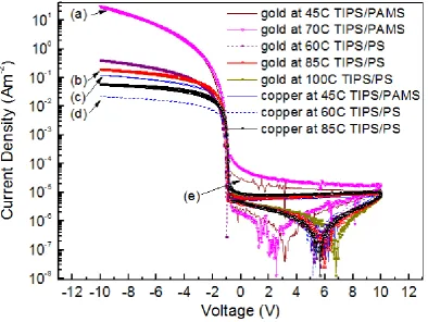
Chapter Three describes the electrical characterization of polycrystalline based Schottky diodes. The active material used is polycrystalline TIPS-pentacene in various blended forms; with plastic binders such as Polystyrene (PS) and Poly-alpha methylstyrene (PAMS), disordered organic semiconductor Polytriarylamine (PTAA) and dopant such as 2, 3-Dichloro-5, 6-dicyano-1, 4-benzoquinone (DDQ). Firstly, the fundamental behaviour of a Schottky diode is discussed followed by an introduction to space charge limited currents. Furthermore, detailed fabrication techniques and their effect on the results are discussed. A simplified expression for the current density in the exponential region of the forward characteristic is shown to determine the characteristic temperature of the intrinsic distribution of carriers. An extension of space charge limited current expression incorporating the universal mobility law is developed to determine the value of the charge carrier mobility. Consequently, various other parameters are obtained from the current-voltage (I-V) characteristics. Furthermore, the variation of I-V characteristics with temperature for two different blends of TIPS-pentacene such as TIPS/PTAA and doped TIPS/PAMS is conducted. Various parameters extracted in the forward and reverse characteristics show a strong dependent on the measurement temperature. The activation energy for both blends are found by plotting Arrhenius plots of bulk limited current density in saturation and conductivity against temperature. The small signal analysis of the capacitance voltage characteristics (C-V) is also conducted to find the dopant concentration in depletion from the plot of inverse squared capacitance against voltage.
Assuming an exponential distribution of states, the current in the forward direction in the grains is established. Finally, Laplace distribution of states is proposed to explain the density of states in an organic disordered material. The carrier concentration is subsequently explained in terms of Maxwell-Boltzmann statistics and Laplace DOS.
Chapter Five is primarily concerned with the analysis of C-V characteristics of a Metal-Oxide-Semiconductor capacitor. The discussion of conventional MOS capacitor physics is followed by the fabrication process involved in producing the organic MOS capacitors. The effect of frequency and voltage are considered to obtain parameters such as the doping concentration, insulator thickness and threshold voltage from the respective characteristics. Hysteresis is discussed to be due to oxide and interface charges. The effects of photo-oxidation are also briefly considered. An equivalent RC circuit to model frequency-dependent capacitance of MOS capacitor is considered and examined. In addition, an equivalent circuit model is also proposed to find the bulk components. Furthermore, experimentally obtained temperature dependence of the capacitance-voltage characteristics are used to explain the variation in charge transport in polycrystalline organic S1150 based MOS capacitors.
Chapter Six concludes the whole thesis in terms of all the work undertaken and the experimental results obtained. Further prospects for research are also proposed.
1.3 CONTRIBUTIONS
The list below comprises the contributions made in this thesis:
Space charge limited currents (SCLC) is defined in the forward characteristics of the Schottky diode where the mobility values are expected to be quite low.
A model demonstrating the universal dependency of mobility on carrier density is presented for space charge limited currents. Hence, space charge limited current expression including Universal Mobility Law (UML) is developed for disordered organic semiconductors.
Disordered materials are compared with the conventional crystalline solids to define the UML in polycrystalline organic semiconductors.
TC, the ratio of free charge carriers to the total charge carriers in the intrinsic DOS, , MNE, ideality factor and other parameters are extracted.
A large value for ideality factor is consistent with previous experiments on disordered materials. The high value in the range of 3-5 proves that the material is not intrinsic and some trapping effects are taking place. High values of TC and hence MNE are indicative of both the extrinsic and intrinsic traps at room temperature.
A good linear fit to the experimental plot of natural log of the reverse characteristics against quarter powered voltage is observed at room temperature indicative of the barrier lowering due to an external field and the image force. The gradient provides the dopant density which is taken to be numerically equal to the carrier concentration for conduction. The ratio of depletion region width and Debye length is high, suggesting that an abrupt depletion region approximation can be applied.
Temperature effects on the electrical characteristics of two different blends of polycrystalline organic Schottky diodes is conducted, namely TIPS/PTAA and doped TIPS/PAMS. For TIPS/PTAA Schottky diode, as the temperature falls, the values of most parameters remain constant until a critical temperature. The activation energy also remains constant at approximately 0.3eV for various applied voltages in saturation. Below this critical temperature, most parameters are observed todecrease.
For doped TIPS/PAMS Schottky diode, parameters such as effective mobility, carrier concentration, MNE decrease with decreasing temperature. From the Arrhenius analysis, two different activation energies are obtained in the range of temperatures observed. At lower temperature range, the activation energy is seen to be twice that of the one obtained in the higher temperature range.
Dopant concentration is found from the slope of inverse square capacitance against voltage plot.
A two dimensional model for a polycrystalline organic semiconductor based Schottky diode is proposed based on simple two one dimensional cases using Gauss’s law. The grains and the grain boundaries are identified in terms of simple equations and the current density classified for both.
Organic polycrystalline based MOS capacitors show a decrease in the maximum capacitance with the change in frequency of the ac signal and temperature, unlike the conventional inorganic MOS capacitors.
Small signal behaviour for an ideal MOS capacitor is discussed in terms of various equivalent circuits. Parameters such as the thickness of the oxide layer, thickness of the organic semiconducting layer, the series resistance, bulk capacitance and bulk resistance are found from the C-f analysis.
Temperature dependence of the C-V characteristics is also observed for organic MOS capacitors. Either the grain or the grain boundary of the polycrystalline material is expected to dominate. The results provide a temperature value very close to the absolute temperature T instead of the TC. Thus, contrary to what is believed, the ordered grains are seen to dominate.
1.4 REFERENCES
[1] Y. Lin, D. J. Gundlach, S. Nelson, and T. N. Jackson, IEEE Device Lett. 18, (1997) 606. [2] A. Dodabalapur, L. Torsi, and H. E. Katz, Science 268, (1995) 270.
[3] C. D. Dimitrakopoulos, S. Purushothaman, J. Kymissis, A. Callegari, J. M. Shaw, Science 283, (1999) 822.
[4] J. H. Schoon, S. Berg, C. Kloc, B. Batlogg, Science 287, (2000) 1022.
[5] D. H. Kim, Y. D. Park, Y. Jang, H. Yang, Y. H. Kim, J. I. Han, D. G. Moon, S. Park, T. Chang, M. Joo, C. Y. Ryu, K. Cho, Adv. Mater. (Weinheim, Ger.) 15 (2005) 77.
[6] H. Sirringhaus, P. J. Brown, R. H. Friend, M. M. Nielsen, K. Bechgaard, B. M. W. Langeveld Voss, A. J. H. Spiering, A. J. Janssen, E. W. Meijer, P. Herwig, D. M. de Leeuw, Nature, London 401 (1999) 685.
[7] W. Zhang, J. Smith, R. Hamilton, M. Heeney, J. Kirkpatrick, K. Song, S. E. Watkins, T. Anthopoulos, I. Mc Culloch, J. Am. Chem. Soc. 131, (2009) 10814-10815.
[8] S. K. Park, T.N. Jackson, J.E. Anthony, D.A. Mourey, Appl. Phys. Lett. 91, (2007) 63514. [9] F.C. Krebs, K. Norreman, Prog. Photovol. Res. Appl. 15, 8 (2007) 697.
[10] J. Meyer, P. Görrn, F. Bertram, S. Hamwi, T. Winkler, H-H. Johannes, T. Weimann, P. Hinze, T. Riedl, W. Kowalsky, 21, 18 (2009) 1845.
CHAPTER 2- CHARGE TRANSPORT MECHANISMS IN
ORGANIC MATERIALS
2.1 INTRODUCTION
Organic semiconductors are promising materials for electronics and opto-electronic devices as they provide opportunities for low cost, large area applications. The charge transport mechanisms in organic materials are under constant debate. Various charge transport models have been developed to describe the conduction in disordered organic materials for example, with good agreement to experimental data. Some of such fundamental models are discussed in this chapter. Interest in disordered organic semiconductors is vital in understanding the conduction mechanisms in polycrystalline organic materials. The majority of this thesis is based on understanding polycrystalline materials, which is believed to consist of grains that are ordered and grain boundaries that are similar to disordered materials. Although the conduction is expected to dominate in the ordered grains, the grain boundaries however limit the flow of the charge carries. Thus, understanding charge transport in terms of disordered organic semiconductors is important for defining charge transport in polycrystalline materials.
2.2 ORGANIC MATERIALS
The interest in organic materials for use in various electronic applications stemmed from the limitations of commonly used inorganic materials such as silicon. Although silicon has good characteristics, the applications are normally based on rigid substrates such as glass and are expensive to produce. Unlike organic semiconductors, its fundamental properties render it unsuitable for the majority of opto-electronics applications such as the lasers used in optical communications. Although cheap information-storing devices like smart cards and inventory control tags can be made, amorphous silicon requires a glass substrate and is not practical in use. In 1950s work on crystalline organics materials started as an alternative to silicon [1]. Although plastic is a very poor conductor of electricity, joint Nobel prize winners Heeger, MacDiarmid, and Shirakawa, in 1970s, demonstrated that polyacetylene backbone can be tweaked to enhance its conductivity. Consequently, later in 1980s, results on first efficient organic LEDs (OLEDs) were published by Kodak and independently results on the first organic transistors (OTFTs) were also made public. Friend et al. at Cambridge University further published the first results on polymer light emitting diodes in 1990s [1].
and small molecules. This has been immensely focused on the development of innovative synthesis and fabrication techniques. The advantage of using organic materials in integrated circuits is that plastic devices are lighter, cheaper than conventional semiconductors, and can be used in optoelectronics. It can also be used for storage and displays as organic materials consume less power. Displays, using OLEDs, are of particular interest in organic electronics as they can be developed on large areas and flexible substrates. Fully flexible displays can be developed where the active matrix is designed of OTFTs instead of amorphous silicon TFTs and the pixel elements are made of OLEDs instead of devices such as LCDs.
OTFTs are another field of innovative research for their application in displays, radio frequency information (RFID) tags and smart cards. A large number of researches continue to advance in order to improve the operational speed of plastic transistors, which is attributed to the charge carrier mobility of the organic semiconductor. Recently, OTFTs based on small molecules have demonstrated high performance with charge mobilities comparable to amorphous silicon transistors existent in display industry. Organic materials offer attractive attributes at a fraction of the cost of silicon.
Organic solar cells with efficiencies of more than 5% have been demonstrated and are attractive due to their compatibility with large area and low temperature processes, thus resulting in lower processing cost than that of silicon. The main advantage of using organic semiconductors is that molecules and polymers can be tailored to include specific electronic or optical properties. Despite such attractive features, organic materials face a constant challenge in terms of electrical and optical stability. They are also attributed to low carrier mobility even with the addition of dopant ions. Furthermore, the processing steps required for developing organic devices are somewhat different from the classical processes in semiconductor industry.
In this thesis, two main organic semiconductors namely Polytriarylamine and TIPS-pentacene are studied. In the following section, their respective chemical structures and electronic properties are briefly discussed, and used in the subsequent chapters.
2.2.1 Disordered Organic Semiconductor
to understand and define its basic electrical properties, operating conditions and conduction mechanisms.
[image:28.595.203.363.308.445.2]In the time-of-flight experiments conducted by Newman [4], bulk mobilities of more than 10-2 cm2V-1s-1 have been observed for PTAA. The basis for high mobility was regarded to be dueto low concentrations of bulk or interface traps. Moreover as PTAA forms a smooth layer, no effects of crystal interfaces are observed [5]. Experimental work on PTAA-based field-effect transistors (OFET) reported hole mobilities of 10-3cm2V-1s-1 in ambient conditions [6]. The bulk mobility value, usually lower, is observed to be higher than the field-effect mobility in PTAA-based experiments mentioned above.
Figure 2.1. Chemical structure of Polytriarylamine PTAA.
2.2.2 Polycrystalline Organic Semiconductor
Pentacene is a p-type semiconductor related to the groups of small molecules. It has a herringbone structure with a combination of edge-to-face and face-to-face molecular interactions which limits the bulk mobility. The performance of pentacene based device can be improved by altering the molecule to form molecular crystals with increased p-orbital overlap.
molecular interactions. TIPS-pentacene has enhanced p-orbital overlap and a reduced inter-planar spacing compared to unmodified pentacene (Fig.2.2).
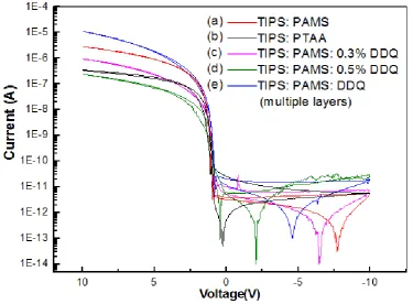
[image:29.595.225.391.324.504.2]Like most polycrystalline organic semiconductors, TIP-pentacene [8, 9] is acclaimed to have higher mobility, compared to the disordered organic semiconductors such as polytriarylamine (PTAA) and poly3-hexylthiophene (P3HT) [10, 11]. Nonetheless, the mobility of the disordered counterparts can be enhanced by extrinsically introducing controlled amount of dopants such as 2, 3-Dichloro-5, 6-dicyano-1, 4-benzoquinone (DDQ) as previously reported by Brown et al. [12] and Raja et al. [13]. In this thesis, experimental analysis on TIPS-pentacene will be carried out to highlight that an increase in conductivity is associated with the addition of dopants. Furthermore, additional experimental work is carried out on TIPS-pentacene and PTAA blend.
Figure 2.2. Chemical structure of 6, 13triisopropylsilyethynyl pentacene (TIPS -pentacene)
2.3 DISTRIBUTION FUNCTIONS FOR OCCUPANCY OF
THE
CARRIERS
The probability of particles occupying available energy levels in a certain system can be described in terms of the probability distribution functions. Such functions include the Fermi-Dirac (F-D) probability, the Bose-Einstein (B-E) and the Maxwell Boltzmann (M-B) distributions as described further in this section [14-16]. The probability of occupancy of energy levels by Fermions is defined by the Fermi-Dirac function. Fermions such as electrons are particles with half-integer spin obeying Fermi-Dirac statistics opposed to bosons which have an integer spin. These particles
Bulky Side Group
Pentacene Backbone
are named after Enrico Fermi and Paul Dirac whereas Bosons obey the Bose-Einstein statistics and are named after Satyendra Nath Bose. A quantum mechanical principle called the Pauli Exclusion Principle states that no two identicalfermions may occupy the same quantum state at a given time. For more than one Fermion occupying the same place in space, the properties of each Fermion, such as the spin, must be different from the rest. Therefore, fermions are usually associated with matter while bosons are often force carrier particles.
Addition of Fermions such as the electrons to the energy levels will fill the vacant states in the energy levels. The states in the higher energy levels are filled after the lower energy levels are filled completely. Increase in temperature causes the shift between completely empty states and completely filled states to be gradual instead of being abrupt as demonstrated in Fig.2.3. In thermal equilibrium, the F-D function is the probability that an electron at energy, E, occupies an energy level. The F-D function at temperature T = 0K is given by
Figure 2.3. The Fermi distribution functions at various temperatures. At T= 0K, the
Fermi function has a step like behaviour. Increasing temperature smears the function
out and causes the function to develop an exponential tail.
2.1
where T is the temperature of the system and EFis the Fermi level energy. For energies that are a few kTs above the Fermi level, the F-D function has a value of unity and at Fermi Level (T = 0K), it has a value of half, thus resembling a step function. For energies a few kTs larger than the Fermi
EF
T= 0K
T2
T1 T1 > T2
1
0.5
E
level, the value decreases exponentially with energy. The other distribution functions, such as B-E function fB-E(E) and M-B distribution function fM-B(E) can be defined as follows and are compared to F-D function.
B-E function is
2.2
M-B function is also called the classic distribution function since it provides the probability of occupancy for particles that are non-interacting at lower densities. These non-interacting particles are distinguishable from each other
2.3
where is the Fermi energy (i.e. the chemical potential) which is known only when the density of states and the electron density are known. This is when is halved. The distribution function for Bosons show that can be much larger than 1 in principle.
For small systems in thermal equilibrium with a single energy level, the distribution function is dependent on the density of states. The Fermi level energy can be determined if the carrier concentration n is known. At finite temperatures, n is hard to determine in terms of . If the electron density is small such that is small, Fermi function can be represented by overlooking the 1 in the denominator. This gives the M-B function, only when values are miniscule (i.e. non-degenerate statistics).
2.4 MODELS FOR DENSITY OF STATES (DOS)
2.4.1 Gaussian Distribution
define the charge transport. In 1993, Bassler defined charge transport of a disordered organic semiconductor within the Gaussian DOS [17]. The transport was described by a hopping mechanism of the carriers between discrete energy states within the Gaussian distribution as in Fig.2.4. The hopping rates were given by Miller- Abraham model [18] and the hypothesis of weak electron-phonon coupling was assumed to disregard polaronic effects. Detailed discussion on Miller- Abraham and polaronic model is presented later in this chapter. Positional and energetic disorder is thought to be introduced when the charge hops in a standard arrangement of hopping sites. Gaussian DOS in terms of energy can be explained by [17]
2.4
where is the standard deviation of Energy, is equal to 1 and has the dimensions of , is the variance and is where the energy deviation is maximum.
Hartenstein et al. [19] presented another approach for describing the positional disorder employing the Gaussian distribution model for the DOS but without verifying a distribution function for the electronic coupling between different sites. The hopping sites, in this case, were grouped in clusters with their closest neighbouring sites and the cluster sizes are dependent on the random inter-cluster distances. Limitations include the use of the model at lower dopant concentrations, for which the inter-site distances are very instable.
2.4.2 Exponential Distribution of States
Energy
N(E)
E
FGaussian Distribution
Exponential Approximation
Enhanced Hopping
[image:33.595.114.502.106.361.2]No Hopping
Figure 2.4. Demonstration of Gaussian Distribution of states (GDOS). GDOS can be
approximated to follow exponential distribution at low energy levels as discussed in Section
2.4.2. Hopping, represented by the blue arrows, is thought to follow variable range hopping
(Section 2.5.4). The filled circles represent the charges introduced by both the electrical field
and doping of semiconductor.
Vissenberg and Matters [22], in addition, developed VRH to take into account the filling of localized states with charge carriers in contrast to the one developed by Bassler which is a one particle model. At low carrier densities and low temperatures, the transport properties are said to be in the tail states of Gaussian DOS, approximated as an exponential DOS (Fig.2.4) [24]:
2.5
where is the exponential distribution of the localized states, Nto is the number of states per
volume unit, T0 is the characteristic temperature describing the width of the carrier distribution, k
Fermi level is fixed by the condition that EF >> kT0 . This means that most carriers occupy the sites with energy E <<0 and the condition T < T0 is fulfilled. When T0 < T, the assumption that charge transport is only in the tail of the DOS is invalid.
2.4.3 Laplace Distribution
A widely accepted model for the distribution of states is the Gaussian disorder model through which the carriers hop to produce current as in Section 2.4.1. The efficiency of hopping defines the mobility of the carriers and hence the charge transport as previously discussed in this chapter, Chapter 3 and in Chapter 5. Recently, Eccleston [25] proposed using Laplace distribution of states (L1 DOS) to define the density of states in an organic disordered material. Laplace L1 has also found different variations in electronics, material sciences and physics and can be seen in statistics such as Fermi Dirac and Maxwell Boltzmann statistics.
Gaussian Distribution
Laplace Distribution
Energy
N(E)
E
E
FE
i=0
E
E
N
intrinsic(E)
Figure 2.5. A comparison between Laplace and Gaussian distribution. Laplace distribution has
a thicker tail and a longer pointed peak. is the energy deviation of the maximum from
Fermi level to the centre of the Laplace or Gaussian distribution. is the standard deviation
Section 2.4.4.
In 1774 Pierre-Simon Laplace introduced a continuous probability distribution that has a probability density function called the Laplace distribution. It is a double exponential function as it can be assumed to be two exponential distributions attached back to back. It is the distribution of the difference of two independent exponential random variables with the same mean. The distribution is essentially symmetric about the centre and therefore uni-modal as seen in Fig.2.5. It can be defined in a dimensionless form with a distribution width λ, location and variance 2 2 [26]
2.6
and in terms of energy as
2.7
where is the standard deviation or the width of the Laplace DOS, is the reference energy equal to 1 with units corresponding to such that is dimensionless, is the energy deviation of the maximum and is the variance. E=0 is assumed to be the Fermi level of the intrinsic material. Figure 2.5 demonstrates subtle differences between a Gaussian and Laplace DOS.
2.4.4 Significance of Meyer Neldel Energy in DOS
The MN rule is defined as a constituent of disorder [32, 33] and the shift in the quasi Fermi level with temperature [34]. Meijer et al. [35] and Yelon et al. [31, 36] defined MNR due to characteristic transport mechanism in disordered materials. Theoretical studies proposed by Fishchuk et al. suggest that the width of DOS in the disordered energy band is said to be proportional to Meyer Neldel energy (MNE) [37]. Fig.2.5 shows the width of the distribution as the energy Eσ corresponding for MNE for both Gaussian and Laplace DOS. Furthermore, MNE is further defined in terms of the characteristic temperature attributed to the disordered DOS in Eq. (3.14), Chapter 3.
In organic electronics, this prediction provides a method for evaluation of the amount of energetic disorder in the material as these materials are said to have a large density of localised states with high activation energy [38]. Moreover, MNE can also be applied to polycrystalline organic materials having ordered grains and disordered grain boundaries. Previously, Roberts [39] followed by Cohen et al. [40] defined the MN rule for polycrystalline or amorphous semiconductors derived from an exponential tailing of the majority band states. This theory has been applied in the upcoming chapters.
Conversely, polaron concept has also been used to theoretically justify MNE in different systems. Polarons are defined as an introduction of lattice deformation around a charge carrier. Kemeny and Rosenberg [41] proposed a model for organic semiconductors where electrons or polarons tunnel past intermolecular barriers from activated energy states of the organic molecules. Polaron model is discussed in detail in Section 2.5.3. However, the polaronic effects in a disorder based transport model are neglected because disorder is considered the main reason for localisation of charge in organic semiconductors. In organic semiconductors, the application of this theory is dependent on validating the use of multi-phonon model to explain hopping of carriers in localised states. Higher activation energy is evident in experiments involving multi-phonons. Increase in the activation energy is indicative of the involvement of a number of phonon that creates various conduction paths for charge transport. Furthermore, the activation energy observed in organic disordered materials is in the range of single phonon energy. This is in contrary to the theory that the transport is due to a multi-phonon process.
partial pressure at annealing, the extent of non-stoichiometry, dopant concentration and other techniques all have an effect on the MNE [42].
In conclusion, MNR is a frequent occurrence in disordered organic materials with a pervasive value. However, there is no universal agreement on the basis of MNR as it is argued to be a result of either the charge carriers having a polaronic nature or due to a common DOS in the disordered material.
2.5 CHARGE TRANSPORT MECHANISMS IN ORGANICS
For pure crystal materials with organized molecular crystals, the charge transport is assumed to occur via charge carriers in delocalized states such as that seen in inorganic conventional semiconductors. The model assumes that the mobility in these materials follows an inverse power law with temperature. That is, that the mobility decreases with the increase in temperature like in highly pure crystalline materials observed in the time-of-flight experiments [43]. Although this is true for very low temperatures, the assumption does not withstand the analytical results. Except at low temperatures, the intermolecular distance is always more than the corresponding mean free path which renders it incompatible with diffusion-limited processes. In inorganic semiconductor crystals as in the case of silicon or germanium, the constituting atoms have strong coupling between each other and the delocalization of the electronic states is possible due to long-range ordering. The valence and conduction bands are thus possible with the distance between referred to as the band gap. The conduction band in inorganic crystals can be thermally activated to generate free carriers. These in turn leave positively charged holes in the valence band. The assumptions such as the one-electron limit for inorganic materials [44, 45] are impossible to consider in organic materials due to the large numbers of atoms and molecules.
role. Charge carriers that are localised can either move by charge hopping with temperature or due to an externally applied electric field. However, thin organic semiconductor films have complicated charge transport behaviour due to the spatial and energetic disorder. The conductivity and hence the mobility is dependent on the density of charge carriers, temperature and the electric field.
Charge transport in organic materials has remained a highly controversial topic over the years. Although huge efforts have been dedicated to charge transport in organics [46-49], issues such as the mobility and temperature dependence, have not been adequately determined. The lack of an analytical model has complicated the organic semiconductor device design. The prediction of device models is complex due to an unclear understanding of the physical origin of many parameters and the difficulty to reproduce results.
The charge transport is based on Gaussian distribution of the density of states with energies, as observed by an optical spectrum from the research of Bassler [17], where the charge transport sites are localized [50]. The analysis of hopping mechanism in organic semiconductors is supported by the introduction of transport energy defined as the energy required for maximizing the hopping probability. Transport energy for a carrier is independent on the initial energy of the carrier and helps in deciding mobility edge [51]. Theories for inorganic disorder materials such as the percolation theory [52] and the concept of charge transport defined by transport energy, Etr already exist [23, 51, 53]. In organic semiconductors with low carrier concentrations, the activation of charge carriers to Etrhappens from the Fermi level instead of the equilibrium energy as Etris temperature dependent [23, 52, 54]. A number of charge transport models are considered for organic semiconductors in the following text which include the Miller-Abraham hopping model, percolation model, variable range hopping model and the multiple trap and release model. 2.5.1 Miller Abraham Hopping Model
In disordered organic semiconductors, the lack of an ideal three dimensional periodic lattice makes the charge transport process harder to understand. Unlike conventional semiconductors, the spatial and energetic disorder has no symmetry and the conduction process in terms of valence and conduction band does not necessarily apply. Instead, HOMO and LUMO terms are used to describe the highest occupied and the lowest unoccupied levels respectively. In disordered semiconductors, very low mobility exists due to the existence of localized states N, referred to as
overcome the energy difference between the two localized states by either absorbing or emitting phonons.
(a)
(b)
Figure 2.6.Charge transport mechanism for an inorganic crystal; (a) with band transport and
delocalized free carriers. Disruption in crystal symmetry is given by a bump. (b) with hopping
transport. The lattice vibrations are necessary for a localized carrier, localized due to defects,
disorder or self-localization, to move from one site to another [50].
A number of different hopping models were predicted. Conwell [24] and Mott [55] suggested the process of phonon-induced hopping in regards to metallic conduction in inorganic semiconductors and later, Pines, Abrahams and Anderson [56] suggested the electron relaxation processes. Mott described the hopping transport in a constant density of states (DOS) where the concept of hopping to higher energies and over long distances had equal significance. He linked the conductivity σ to vary with temperature according to the relation
2.8
where , N(0) is the density of states at the Fermi level and b is the size of the localized states [21].
impurity levels with narrow range energy levels. This meant that a higher probability existed for electron to jump to the nearest empty site (Fig.2.6).
The hopping rate of carriers from occupied i to unoccupied j localized donor states depends on the height of the energetic barrier Ej − Ei and the distance Dij between the states i and j
2.9
where the pre-factor ν0is the attempt-to-hop frequency, is the inverse localization length, and k is the Boltzmann constant. represents the tunnelling probability
and represents temperature dependence of the phonon density.
For disordered organic semiconductors, the disordered sections of the material act as isolated states making Eq. (2.9) valid at high temperatures [21]. In inorganic semiconductors at higher temperatures, hopping transport is overcome by band-like transport. This is owing to the inversion of carriers such that they shift from donor states into a higher number of energy levels at the conduction/valence band edge.
Multi-phonon processes have been ignored in this model. These are said to control the charge transport in organic semiconductors if the charge carriers are localised polarons. Charge transport based on polaron model has been discussed in detail in Section 2.5.3. Ignoring multi-phonon processes would lead to an erroneous value from the temperature dependent mobility. However, in disordered materials, considering that weak electron-phonon interactions exist. The polaronic effects can be ignored [17]. A hopping model similar to the Miller-Abraham model was proposed by Bleibaum et al. where they introduced a prefactor dependent on the electron-phonon coupling strength, the phonon DOS and other properties of an organic semiconductor [57].
2.5.2 Percolation Model
Percolation models were first introduced to explain the charge transport in disordered inorganic semiconductors [58]. However, it has also been used to explain charge conduction in organic semiconductors [22, 59]. Charge conduction in organic semiconductors is mainly due to the application of externally applied electric field or hopping between localised states due to thermal activation. The polaronic effects, mentioned in Section 2.5.3, are ignored as they are considered small with regards to energetic disorder. The activation energy required for hopping is not reliant on the molecular conformation energies used to form activated complexes before transfer of charge. It is only dependent on the site energy differences [60] and can be written in terms of Miller-Abraham model, Eq. (2.9). In thermal equilibrium, the hopping rate can be explained to obtain conductance Gmax [61]. Eventually, every hop between localised states in an organic semiconductor can be explained in terms of a unique conductance. This conductance is described by the quasi Fermi energy, the respective site energy and the intermolecular spacing.
organic semiconductor. For a disordered three dimensional system BC~2.8 [62] and is obtained by numerical simulations.
Using Miller-Abraham’s model for conductance introduced in 1960s, the maximum distance, , between two hopping sites between which a hop can occur is given by
2.10
and the maximum energy, , that any initial or final state can have is given by
2.11
where ν0 being the attempt-to-hop frequency. Thus the density of states that can be part of the percolating sub-network, , is presented by
2.12
where is the site density function.
As only the sites within a range are linked together in a sub-network, this criterion can be written in terms of a dimensionless quantity, and can be linked to Mott’s law [63].
2.13
2.5.3 Polaron Model
polymers to change their geometry upon charging. The origin of localisation is therefore due to the formation of polarons.
An individual charge carrier has a coulomb field that first polarises its surrounding and then couples itself to it. The charge therefore has an accompanying deformation which acts like a quasi-particle, also known as a polaron. The charge carrier carries the lattice deformation it induces and the polaron is considered to be self-trapped.
X
X X X X
X
X X X X
n
n (a)
(b)
Figure. 2.7. (a) A heterocyclic polymer where X can be Sulphur (S), Nitrogen (N) or Oxygen
(O). (b) A polaron lattice deformation is established into the conjugated backbone of
heterocyclic polymer. This can be caused by p-type doping causing the loss of an electron [64].
In disordered semiconductors, the extent of interactions is usually constrained by the huge amounts of structural defects. The lattice deformation, unlike in crystalline semiconductors, can therefore be compared with the inter-atomic distances. These lead to strong short range electron-lattice interactions due to the self-trapping of carriers at a single position and are explained as ‘small polarons’. Yamashita and Kurosawa [65] and Holstein [66] were the first to develop the model based on small polaron transport.
Polaron movement is thought to be by a succession of random jumps between neighbouring sites. Marcus [69] defined the transition (hopping) rate, , for polarons in terms of Er, the
intra-molecular reorganization energy,
. 2.14
The charge mobility µ, with field F and temperature dependence T, is defined by the thermally activated hops between adjacent sites i and j [70, 71].
2.15
where is slightly temperature dependent and b is the average lattice difference. Eq. (2.15) expects a thermally activated behaviour for mobility. This is in concurrence with the information that polaronic tansport occurs via thermally induced deformations of the lattice.
Su-Schrieffer-Heeger (SSH) also determined a charge transport model in terms of polarons for conjugated polymers [72]. The theory was derived from bond alteration along an ideal conjugated polymer chain with weak inter-chain coupling. The geometrical structure of the polymer was said to change immensely by the addition of a charge due to bond alteration over a certain number of monomeric units (3-5). Main concerns with using SSH model include the disregard of electron-electron and electron-electron-hole interactions which play an important role in the transport and recombination of charge carriers.
For disordered materials such as conjugated polymers, the charge transport is thought to be through hopping mechanisms. Variable range hopping (VRH) is thought to occur in systems where the thermal energy, kT, is less than the energy variation between successive states. The concept of VRH was first introduced by Mott [55] as discussed in Section 2.5.1 in Eq. (2.8). He assumed that the probability of hopping to higher energies or over far distances was equivalent. The density of states, in this case, is expected to be spread consistently about the Fermi level. VRH mechanism is commonly acknowledged charge transport model applied to organic systems as the energy and positional disorder of localized states in the organic material dominates the charge transport. Vissenberg and Matters defined disordered materials to have VRH in states which vary in energy exponentially [22]. VRH implies that a carrier may either hop over a small distance with high activation energy or hop over a long distance with a low activation energy. This is unlike the idea of hopping where the thermally activated tunnelling of carriers between localized states governs the charge transport instead of carrier activation to a transport level. The mobility is said to increase with carrier concentration by either field effect or doping as an introduction of acceptors in a p-type semiconductor causes a small number of unoccupied states to be filled. Increasing in doping causes more levels of unoccupied states to be filled such that hopping is easier at higher energies when an external voltage is applied and therefore mobilities are higher.
The model then assumed that the mobility in these materials can be thermally activated and depends on the gate voltage according to a power law. As the gate voltage increases, the injected charge carriers fill up the traps such that as a result, the trapping becomes less and the charge transport is seen to improve. This dependence is noticed in disordered materials and is of great importance as it is similar to the one observed from our experimental results on polycrystalline material. It is essential in the analysis of electrical characteristics of organic devices such as the OTFTs, OLEDs and Metal-Oxide-Semiconductor field effect transistors (MOSFETs).
2.5.5 Multiple Trap and Release Model
For organic materials such as the polycrystalline organic semiconductors, model based on multiple trapping and release (MTR) [71-73] with a temperature dependent transport exists [74, 75]. For this model, two separate types of conducting mediums exist; crystalline ordered grains which are separated from each other by disordered amorphous grain boundaries. The grains incorporate delocalized carriers while the grain boundaries contain carriers trapped in localized states. It assumes that delocalised transport is limited near the band gap due to the existence of a distribution of traps. The trapped carriers in the grain boundaries can be thermally activated to a transport level where charge conduction is easier. This charge transport is very similar to the one described above as hopping mechanism. For grain boundaries, the model predicts mobility dependent on temperature which decreases with the improvement in the quality of the devices. The gate bias dependence decreases with increasing quality as well confirming that the defects decrease such as seen in single crystal devices.
Etr
EF
Energy (E)
Distance
trapped and injected charge carriers
Localised states acting as traps
Figure 2.8. Demonstration of multiple trap and release model (MTR). The deep lying localised
states briefly trap the carriers. These carriers can be thermally released to states around the
Horowitz et al. [74] have recently used the MTR model to establish charge transport in organic semiconductors, namely sexithiophenes and dihexylsexithiphenes, based OTFTs with an exponential distribution of gap states, initially derived from MTR model applied to an inorganic material by Le Comber and Spear [71]. The MTR model accounts for the low mobility in amorphous organic materials. Hopping of charge carriers between localised states is dominated over a critical level known as the transport energy, Etr which defines the mobility edge as shown in Fig.2.8. Trapping is associated with lattice defects and impurities in which the charge carriers are immobilized and confirms a narrow band gap with high trapping. Traps can either be shallow or deep; shallow traps related with the conduction or valence bands and deep traps situated near the centre of the band gap.
The existent organic semiconductor charges or the injected charges are all trapped and then released by thermal activation process. Ignoring the diffusion processes, the drift mobility can be defined in terms of the energy of the trap states Et, the mobility at band edge and the ratio between the effective density of states at the transport band edge and the density of traps, α.
2.16
Eq. (2.16) predicts an Arrhenius- like temperature dependence on the carrier mobility, like the VRH model. The transport of carriers is, therefore, seen to be greatly dependent on the level of energy of the trap states, the externally applied voltage and the temperature [74].
2.5.6 Charge Transport in Polycrystalline Organic Semiconductors