Abstract: The improvement in impedance type DC-AC converter with step up voltage is achieved by the inclusion of new type of On/OFF capacitor. Impedance source inverter is used to step up and step down the input voltage. Impedance source DC-AC converter is used to decrease the effect of wide change in electrostatic effects for the capacitor used. To have better step up voltage without change in switches initially impedance source inverter is proposed. The proposed circuit overcomes the disadvantages of traditional impedance source inverter.
Keywords: THD; boost; shoot through; non shoot through
I. INTRODUCTION
Impedance Source inverters has advantages over the conventional inverters like voltage source inverter and current source inverter. The conventional inverters cannot able to step up the input voltage. But due to the impedance source inverter the voltages can be stepped up and stepped down simultaneously. The range of voltage buck-boost ratio is obtained through formula. The author [1] discussed in detail about the concept of Z-source inverter. Step up control of maximum control of the impedance source inverter is suggested in [2]. The control circuit for impedance source inverter [3] was discussed. To minimize current ripple and voltage handling capability in terms of stress has been proposed with fixed step-up control for impedance source inverter [4]. For service main with photo voltaic [5] system was developed using impedance source inverter. Three phase Z-source inverter are proposed and implemented [6]. The analysis is made on the modulation schemes. Advanced impedance source inverter was developed [7] using special type of inductor. Further the family of impedance source inverter was developed with two inductors [8].
Revised Manuscript Received on March 08, 2019.
Chinnapettai Ramalingam Balamurugan, Department of Electrical and Electronics Engineering, Karpagam College of Engineering, Myleripalayam Village, Othakkalmandapam, Coimbatore, 641032, India
R.Kalai Surya, Department of Electrical and Electronics Engineering, Karpagam College of Engineering, Myleripalayam Village, Othakkalmandapam, Coimbatore, 641032, India
N.Kayalvizhi, Department of Electrical and Electronics Engineering, Karpagam College of Engineering, Myleripalayam Village, Othakkalmandapam, Coimbatore, 641032, India
M.Raouf Khan, Department of Electrical and Electronics Engineering, Karpagam College of Engineering, Myleripalayam Village, Othakkalmandapam, Coimbatore, 641032, India
P.Santhosh, Department of Electrical and Electronics Engineering, Karpagam College of Engineering, Myleripalayam Village, Othakkalmandapam, Coimbatore, 641032, India
The circuit discusses about five level h type multilevel inverter using control freedom degree pulse generation technique. For renewable energy systems [10] the recent power conditioning system was developed using Quasi impedance source inverter with modeling and control. Development of reduced cost phase conversion converter using step up technology [11]. To develop photovoltaic applications embedded inverter are recent topologies that can perform both buck/boost functions are used [12]. To suggest [13] an impedance source inverter with different loads the simulation study was carried out and analysed its performance. For different loads the developed inverter has the additional step up capacity to increase the voltage [14]. With different configurations of voltage stress and low value of L, the inverter will have better performance [15]. A hardware is developed for ON/OFF configuration of inductor with Z network [16]. H-bridge inverter fed AC motor using SPWM technique is implemented [17]. A detailed study is made on various power circuits and control topologies of proposed inverters [18,19]. The single phase switched inductor switched capacitor type inverter is developed by [20]. The new type of cascaded Z source neutral point clamped inverter is developed [21]. For voltage step applications [22] new impedance source inverter was developed. Digital control is designed using MATLAB coding for new impedance source inverter.
II. PROPOSED METHOD
Switched Capacitor Z Source Inverter can be realized by replacing the inductor cell with a capacitor cell with small modifications in the positions of the passive Switched Capacitor Z Source Inverters with Extended Boost Capability components. This proposed topology has overcome the existing topologies constraints. The advantages of the proposed method are boost factor increases as the number of (n) cascaded cells increases, It provides high gain, It minimize the ripple current within the inverter, Efficiency of the system can be improved, Reduces the voltage stress across the capacitors during initial conditions and It reduces the THD value.
III. SIMPLE BOOST CONTROL
In this technique or methods the time durations are represented by two constant lines. The line magnitude will be higher or lower than the maximum of the reference wave.
Performance Analysis of Extended Boost
Switched Capacitor Impedance Type DC-AC
Converter
Fig. 3 displays the MATLAB tools to create gate pulses
[image:2.595.158.414.90.360.2]by comparing the reference and carrier signals.
Fig. 1 Gate pulse generation Reliability Calculation
Formulae to find reliability of a inverter is
P =
B
T
A
B
S
Q
E failure/106 hrs IGBT used for calculation is = KGT 25N120NDA(i) Calculate the reliability for switched capacitance with
600
120
V
A
IGBT
B = 0.00074
R = 62.7
T = 5.9
S = 0.39
A = 0.7
Q = 0.7
E = 6.0
P ,IGBT = 0.3138 failure/106 hrs Use 6 IGBT ,
P ,INV = 6*0.3138= 1.8828 failure/106 hrs
[note: Failure rate =
1
P
] Mean time to failure ,MTTF =
1
P
,INV=
1
1.8828
= 0.53112 Mean time to failure,
MTTF = 531123 hrs
(ii) Calculate the reliability for switched capacitance with
600
25
V
A
IGBT
P =
B T
A
B
S Q
E failure/106 hrs
B = 0.0007
R = P0.37
T = 5.9 S = 1
A = 0.7
Q = 2.4
E = 6.0
P ,IGBT = 0.0007*5.9*0.7*(600*25)0.37 *2.4*6 = 0.007*5.9*0.7*35.08*1*2.4*6
P ,IGBT = 1.46 failure/106 hrsUse 6 IGBT ,
P , INV = 6*1.46= 8.76 failure/106 hrs
[note: Failure rate =
1
P
]Failure rate =
1
P
=
1
8.76
*106 hrs
= 0.114155251 hrs Mean time to failure,
[image:2.595.43.538.91.828.2]Reliability in years =
114155
365* 24
= 13yrs
Switching Power Device Calculation Formula used:
Total average SDP=(SDP)av= 1
N M
Vmlm-averageTotal peak SDP =(SDP)pk = 1
N M
Vmlm-peakThe average and peak SDPs of Z-source inverter are Given data:
Po=152*13=1976 watts M=1
cos
=1(SDP)av = (2Po(2-
3
M)/(3
M-1)+(43
P0/cos
))= (2(1976)(2-
3
(1))/(3
(1)-1)+4*
3
*1976)/cos0o*
)= (3952)(0.267)/(0.732)+13690/3.141 = 1055.184/13960.732/3.141
(SDP)av =
8
max oi
V
P
cosV m
=
8*105*1.9761
1*100* *1
(SDP)av = 5.283 KVA
Ip=
3
o
p
p
cos V
=
3
1.976 *10
3*1*
V
pthen,
Vp =
2 2
i
V
*M
Vp =
100
2 2
*1Vp = 35.35
Ip =
3
1.976*10
3*1*35.35
= 18.632 Amps
IPK =
2 *18.632
IPK = 26.35 Amps (SDP)pk = 6*Vs*Ipk
=
max
8
*
cos
*
*
o i
V
p
V
M
= 38*105*1.976*
1*1
10
00*1
(SDP)pk = 16.60 KVA
LC Filter Design GIVEN:
p
V
=57.73
V
dc=98.10P
n =120 WL
I
=7.6 A
f
s=2*103 Hzresonant frequency
=
1
2
of switching frequency Fsw
Solution
2
(
p)
b h
v
Z
P
2(57.73)
120
=27.7721
1
2
*
bn b b
C
W Z
f
Z
1
2 *50* 27.77
Cb =1.146*10-4 F
0.1*
3
2
n L max phP
I
V
0.1*120*
3*5
2
7.73
=0.097 A16*
*
dc i s L
V
L
f
I
398.10
16* 20*1
0
*0.09
7
i
L
= 3.16mH
f
C
= 0.05*C
b=0.05*1.146*10-4
f
C
=5.73
F
*
*
i g
ref
i g f
L
L
W
L
L
C
3 3 3 63.16*10
10*10
3.16*10 *
*5.73*10
g g
L
L
3 10 83.16*10
10*10
1.8106*10 *
g gL
L
1810.68*
L
g1810.68*
L
g -L
g = 3.16*10-3g
L
(1810.68-1) = 3.16*10-3
3
3.16*10
1810.68 1
g
L
3 6
3 6 6
3.16*10
1.746*10
3.16*10 *1.746*10 *5.73*10
res
W
11
1.0000 *10
9
= 316242.7
res
W
= 316.242
kHz
3*
1
*
sd
res f
R
W
C
1
3 61
3*316.242*
0
*5.73*
10
sd
R
=0.1839
2 *
sd f
s
R
L
f
2
30.
*
18
0
39
20*1
L
f
1.46*10
6H
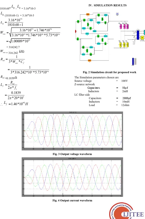
[image:4.595.47.549.38.798.2]IV. SIMULATION RESULTS
Fig. 2 Simulation circuit for proposed work The Simulation parameters chosen are
Source voltage = 100V Z-source network
Capacitors = 50μf Inductors = 2mH LC filter side
[image:4.595.304.556.71.268.2]Capacitors = 2000μf Inductors = 10mH Load = 12ohm
Fig. 3 Output voltage waveform
Fig. 5 Output voltage total harmonic distortion
Table. 1 Comparison of various performances with different topology Topology
Name Input Voltage
Output Voltage
Output Current
VTHD %
VSI 100 63.1 5.3 0.46
ZSI 100 153.35 13 2.7
EZSI 100 155.9 13.3 2.35
EBSCZSI 100 157.7 14 1.71
V. CONCLUSIONS
The proposed extended boost switched capacitor Z Source inverter have better voltage gain characteristics and less THD values . It is to be appreciated that Z Source inverters are flexible for various modifications and can be applied to the entire spectrum of power conversion which finds applications in renewable energy and motor drives. It is also evident that much new class of Z Source inverters is possible with suitable modifications either in topological design and/or modulation schemes for the above applications, if required.
REFERENCES
1. Peng, F.Z. (2003) „Z-Source Inverter‟, IEEE Transactions on Industrial Application, Vol. 39, No. 2, pp. 504–510.
2. Peng, F. Z., Shen, M. and Qian Z.(2005) „Maximum Boost Control of the Z-Source Inverter‟, IEEE Transactions on Power Electronics, Vol. 20, No. 4, pp. 833-838.
3. Loh, P. C., Vilathgamuwa, M., Lai, Y. S., Chua, G. T. and Li Y. W. (2005) „Pulse Width Modulation of Z Source Inverters‟, IEEE Transactions on Power Electronics, Vol. 20, No. 6, pp. 1346-1355. 4. Shen, M., Wang, J., Joseph, A. and Peng, F. Z. (2006) „Constant Boost
Control of the Z-Source Inverter to Minimize Current Ripple and Voltage Stress‟, IEEE Transactions on Industry Applications, Vol. 42, No. 3, pp. 770-778.
5. Huang, Y., Shen, M., Peng, F.Z. and Wang, J. (2006) „Z-source inverter for residential photo voltaic systems‟, IEEE Transactions on Power Electronics, Vol.21, No. 6, pp. 1776–1782.
6. Thangaprakash, S. and Krishnan, A. (2010) „Implementation and Critical Investigation on Modulation Schemes of Three Phase Impedance Source Inverter‟, Iranian Journal of Electrical & Electronic Engineering, Vol. 6, No. 2, pp. 84-92.
7. Zhu., M. (2010) „Switched Inductor Z-Source Inverter‟, IEEE Transactions on Power Electronics, Vol. 25, No. 8, pp. 2150-2158. 8. Nguyen, M.K., Lim, Y.C., Choi, J.H. (2012) 'Two Switched Inductor
Quasi Z-Source Inverters', IET Power Electronics, Vol. 5, No. 7, pp. 1017-1025
9. Subramanian, D., Rasheed, R. (2013) 'Five Level cascaded H-Bridge Multilevel Inverter Using Multicarrier Pulse Width Modulation Technique', International Journal of Engineering and Innovative Technology, Vol. 3, No.1, pp. 438-441.
10. Dinakaran, C., Panthee, A.B., Eswaramma, K. (2014) 'Modelling and Control of Quasi Z-Source Inverter for Advanced Power Conditioning of Renewable Energy Systems', International Journal of Advanced Research in Electrical, Electronics, and Instrumentation Engineering, Vol. 3, No.2, pp.136-141.
11. Khosravi, F., Azli, N.A., Kaykhosravi1, A. (2014) 'Design of Reduced Component Count Single Phase-Three Phase quasi Z-Source Converter', IET Power Electronics, Vol.7, No.3, pp. 489-495 12. Kohila, J., Munia Raj, R., Kannan, S. (2014) 'Z Source Multilevel
Inverter for Photovoltaic Application', International Journal of Innovative Research in Science, Engineering and Technology, Vol. 3, No. 3, pp. 492-297
13. Chougule. G., Gaikwad, A. (2015) 'Simulation Study of Quasi Z-Source Inverter for Resistive and Inductive Load', International Journal of Innovations in Engineering Research and Technology, 2015, Vol. 2, No. 6, pp.2-13
14. Elakya, V.C., Aarthi., Teresa, V.V. (2015) 'High Performance Extended Switched Inductor Quasi Z-Source Inverter for Three Phase Loads', International Journal of Innovative Research in Science, Engineering and Technology, Vol. 4, No. 4, pp. 76-81
15. Yang, L., Qiu, L., Zhang, B. (2015) 'High-Performance Quasi Z-Source Inverter with Low Capacitor Voltage Stress and Small Inductance ', IET Power Electronics, Vol.8, No.6, pp. 1061-1067
16. Jackson, E.S. (2016) 'Implementation of Switched Inductor Quasi Z-Source Inverter', International Journal of Pharmacy and Technology, Vol.8, No.4, pp.23769-23779
17. Bhujangaro, Y., Bhavani, T. (2016) 'Implementation of Cascaded H-bridge Multilevel Inverter for Sinusoidal PWM Controller Fed Induction Drive', International Journal of Advanced Technology and Innovative Research, Vol.8, No.9, pp.1870-1876
18. Shehu, G.S., Kunya, A.B., Shanono, I.H. (2016) 'A Review of Multilevel Inverter Topology and Control Techniques', Journal of Automation and Control Engineering, Vol.4, No.3, pp.233-241. 19. Himanshu., Khanna, R., Jain, N., (2016) 'A Survey on Various
Topologies of Z-Source Inverters', International Journal of Electrical and Electronics Engineering, Vol.3, No.7, pp.5-9.
[image:5.595.98.497.256.340.2]21. Yuyao, He., Hailong, Liu., Wei, F., (2016) 'Novel Cascaded Z-Source Neutral Point Clamped Inverter', Chinese Journal of Electronics, Vol.25, No.5, pp. 965-973.
22. Mubeen, M. (2016) 'Design of Z-Source Inverter for Voltage Boost Applications', International Journal of Innovative Research in Electrical, Electronics, Instrumentation and Control Engineering, Vol.4, No.2, pp. 136-140.
23. Vijayalakshmi, K., Balamurugan, C.R. (2017) „Z Source Multilevel Inverter Based on Embedded Controller‟, TELKOMIKA Indonesian Journal of Electrical Engineering and Computer Science, Vol.6, No.1, pp.1-8.
Biographical notes: Chinnapettai Ramalingam Balamurugan was born in 1978 in Kumbakonam. He has obtained B.E (Electrical and Electronics), M.E (Power Electronics and Drives) and Ph.D (Instrumentation Engineering- Power Electronics) degrees in 2000, 2005 and 2015 respectively from Arunai Engineering College, Tiruvannamalai, Sathyabama University, Chennai and Annamalai University, Chidambaram. He has been working in the teaching field for about 14 years. His areas of interest include power electronics, electrical machines and solar energy systems. He has 110 publications in international journals. His research papers 80 have been presented in various/IEEE international/national conferences. Currently, he is working as Professor and Head in the Department of EEE, Karpagam College of Engineering, Coimbatore. He is guiding 7 Ph.D scholars under anna university, Chennai. He got best faculty awards for nearly five times. He wrote more than thirty books. He is the reviewer for many reputed journals. He is a life member of Instrument Society of India and Indian Society for Technical Education. He is a member in IEEE. He cleared NPTEL certification Course. Received “DIGITAL GURU AWARD AND CASH PRIZE” for valuable contributions towards the digital content developed for Power Electronics.. Contact number- +91-9894522351. E-mail: crbalain2010@gmail.com.