Rochester Institute of Technology
RIT Scholar Works
Theses Thesis/Dissertation Collections
6-1-2012
A Coarse imaging sensor for detecting embedded
signals in infrared light
Mark Bailly
Follow this and additional works at:http://scholarworks.rit.edu/theses
This Thesis is brought to you for free and open access by the Thesis/Dissertation Collections at RIT Scholar Works. It has been accepted for inclusion in Theses by an authorized administrator of RIT Scholar Works. For more information, please [email protected].
Recommended Citation
A coarse imaging sensor for detecting embedded signals in infrared light
by
Mark S. Bailly
A Thesis Submitted in Partial Fulfillment of the
Requirements for the Degree of
Master of Science
in
Electrical and Microelectronic Engineering
Approved by:
_________________________________________________ Advisor: Dr. James E. Moon
_________________________________________________ Member: Dr. Robert J. Bowman
_________________________________________________ Member: Dr. Mark A. Hopkins
_________________________________________________ Department Head: Dr. Sohail A. Dianat
Department of Electrical Engineering
Kate Gleason College of Engineering
Rochester Institute of Technology
Rochester, New York
ii ACKNOWLEDGEMENTS
Thank you Dr. James Moon, Dr. Mark Hopkins, and Dr. Robert Bowman for generously
serving on my thesis committee and for all the valuable assistance and support you have
provided to me on this project. The Electrical Engineering Department has my thanks for their
advice, logistical support, use of equipment, and other resources.
This thesis was funded and supported by Timothy Hoskins and Michael Grimm. Their
financial support made the purchase of components and the machining of a prototype possible.
Help from the Multi-disciplinary Senior Design team was invaluable in the creation of
schematics and lengthy test procedures. Brian Rella and Andy Middleton were invaluable in this
capacity as well as their guide, Gerald Garavuso. Additionally, help from Alex Coleman in the
programming of the microcontroller for the control and capture of data on the prototype made
iii
Abstract – The use of machine vision has become prevalent in touch technology. However, it is
still limited by background noise. To reduce the background noise present in the images of
interest, it is important to consider the imaging device and the signal source. The architecture,
size, sampling scheme, programming, and technology of the imaging device must be considered
as well as the response characteristics of the signal source.
Several pixel architectures are explained and implemented with discrete components.
Their performance was measured through their ability to track a modulated signal source.
Potentially, an imaging sensor comprised of a system designed to modulate the light to be
imaged could drastically reduce background noise. Further, with a less noisy image, the
iv
TABLE OF CONTENTS
Page(s)
Acknowledgements………...………...ii
Thesis Abstract………...iii
Section 1: Analysis of photosensitive devices and pixel architectures…..1-32
Abstract……….………2
Introduction……….………...3-5
Theory………..6-15
Experimental………..……15-29
Conclusion………..30
Section 2: Analysis of discrete component implemented pixels…...…...33-76
Abstract……….………..34
Introduction……….………...34-35
Experimental………..……35-75
Conclusion………..76
Section 3: Identifying and tracking objects in a simple background….77-100
Abstract……….………..78
Introduction……….………...78-79
Theory………80-97
Experimental………..……97-99
Conclusion………100
Section 4: Creating and testing a coarse surface imaging sensor for
ROCHESTER INSTITUTE OF TECHNOLOGY
Analysis of photosensitive devices and pixel
architectures
Section 1
Section 1 Page 2 of 113
Abstract – High-density image sensors were originally dominated by charge-coupled devices
(CCDs) that require specialized processes to limit dark current and enhance charge transfer
efficiency, as opposed to the passive pixel sensors (PPS) which can be fabricated through
standard CMOS processes. As of the early 1990s the minimization of device sizes made a new
type of imaging sensor practical, the active pixel sensor (APS). Like the PPS, the APS may be
fabricated with standard CMOS processes, only in addition to a photosensor and a switching
transistor, the APS integrates an amplifier at every pixel location. Further device miniaturization
allows for the creation of digital pixel sensors (DPS) which integrate analog to digital converters
(ADC) at every pixel location in addition to amplification. The DPS is capable of massively
parallel readout and high-speed data transfer, allowing for high-speed imaging of over 10,000
frames per second.
While the integration of more and more transistors at each pixel location is possible
without significantly affecting the sensing area to pixel area ratio (fill factor), it is important to
consider the impacts of non-ideal effects introduced by the sub-micron transistors. As such, it is
important to consider the advantages and disadvantages associated with each technology and find
the technology that best suits the specific application. This paper will focus on exploring those
advantages and disadvantages in an effort to find the best system for a large-area high-speed
Section 1 Page 3 of 113 I. Introduction Column Amplifiers R o w D ec o d er s Column ADC/Mux Horizontal CCD V er ti ca l C C D Output Photodiodes Interline CCD Output Photodiodes CMOS
(a) (b)
Figure 1. (a) CCD array architecture and (b) APS array architecture. Adapted from: [1] © 2005 IEEE
CCDs use specialized process technologies in order to function properly. This process is
designed to allow for device scaling without significant reduction in performance. Any increase
in the flow of dark current or loss to the efficiency of the charge transfer mechanisms will reduce
the device’s performance. The use of gettered, high-resistivity wafers to reduce traps from
metallic contamination and buried channels with multiphase pinned operation are common
techniques for reducing surface-generated dark current. The array relies upon shifting charge
packets out of the array one by one. In Figure 1(a) the CCD imager uses a vertical architecture to
shift charge packets downwards and then a horizontal architecture to shift those charges out to
the right. Once each charge is shifted out of the array it is converted to a voltage and read out of
the system. This architecture creates very minimal pixel overhead, allowing for high fill factors
despite miniaturization. Although this architecture makes addressing pixels simple when
compared to the APS, it increases the impact of dark current on the system. Dark current not
Section 1 Page 4 of 113 system must undergo in order to fully read the system. While CCDs traditionally have orders of
magnitude less dark current than APSs, they have an increased sensitivity to it.
CMOS imaging sensors require a more complex addressing scheme. Typically charge is
read out as a voltage by activating a single set of row-select transistors and is then digitized
either in serial or in parallel by ADC(s) as in Figure 1(b). This allows for some system
parallelization as the columns may be read simultaneously, allowing for potentially faster
operating speeds than can be achieved with CCD arrays. Due to the lack of charge transfer
between pixels, this system may tolerate much higher levels of dark current. Further, the CMOS
imaging sensor may integrate the analog and digital circuitry on the same chip, creating a lower
power and overall smaller device. In addition to the readout circuitry, other functional processes
may be integrated into the system to mitigate parasitic effects and enhance imaging performance
[1].
Figure 2. Cross sectional SEM photograph of an image sensor [1] © 2005 IEEE
Regardless of the type of imaging sensor, structures similar to Figure 2 are used to
Section 1 Page 5 of 113 light at more extreme angles to be focused onto a small active region, thereby increasing the
photocurrent iPH for each sensor and improving the signal-to-noise ratio (SNR). Depending on
the characteristics of the active region in the sensor, there are varied sensitivities to different
wavelengths of light. In order to effectively bias the sensors so that they selectively image a
particular color, color filters may be implemented to skew the device’s external wavelength
sensitivity.
Under normal illumination conditions, the CMOS imaging sensor photocurrents are too
small to be read directly.
VD
Reset Light
CD
High light
Low Light
Figure 3. (a) Example schematic of a pixel operating in integration mode
(b) Charge versus time for two different illumination levels. Adapted from: [1] © 2005 IEEE
The charge-up and release configuration in Figure 3 (a) is implemented with an integration time
to increase the magnitude of the charge collected for any level of illumination. While this allows
for lower levels of illumination to be detected, it also sets a maximum level illumination that can
be read. As can be seen from Figure 3 (b), under high levels of illumination the charge in the
capacitor saturates, limiting the maximum detectable signal. The effects of well saturation may
be mitigated by adjusting the integration time of the pixel, but this will also increase the
Section 1 Page 6 of 113 II. Theory
A) Noise
Image sensors suffer from non-idealities that limit their performance. Temporal noise and
fixed pattern noise (FPN) are two major concerns. Temporal noise includes shot, pixel reset,
thermal, flicker, and quantization noise. Due to its active read nature, there are more sources of
temporal noise in CMOS sensors than in CCD sensors. FPN consists of two types, offset FPN
and gain FPN. Offset FPN is more easily corrected for as it is signal-independent, unlike gain
FPN which is signal-dependent.
Active amplification present in CMOS sensors introduces more gain FPN than is
observed in CCD arrays. Mismatch in transistors leads to changes in the gain of each pixel, or
gain changes between columns of pixels, depending on the amplification scheme of the array.
Correlated Double Sampling
Q
t S1
S2
(a)
Delta-Reset Sampling
S3 S2
(a)
t Q
Figure 4. (a) Correlated Double Sampling technique
(b) Delta-Reset Sampling technique. Adapted from: [1] © 2005 IEEE
As mentioned earlier, offset FPN may be compensated for. Correlated double sampling (CDS)
achieves this but requires that two samples of the signal be taken for each pixel, as seen in Figure
4 (a). Although offset FPN is reduced through this process, read noise is doubled from flicker
noise. Therefore, it is only sensible to use this technique when the read noise is less than half the
Section 1 Page 7 of 113 integration time— with the obvious limitation of minimal detectable signal. CDS does not
correct for dark signal non-uniformity (DSNU), as it varies with temperature or gain FPN.
The three-transistor APS is not capable of true CDS and must use delta-reset sampling
(DRS) as shown in Figure 4(b). Although this technique may serve to reduce the offset FPN, the
offset FPN after reset may not be the same.
B) SNR and dynamic range (DR)
Presuming that the offset FPN has been successfully suppressed, the average noise power
may be expressed as the sum of shot noise , read noise , DSNU , and
photo-response non-uniformity (PRNU) . This allows for the SNR to be characterized as
[
( ( ) )] (1)
where q is the electron charge and tint is the integration time. From (1) it can be seen that an
increase in tint results in an increase in the SNR, but it is important to consider that it limits the
Section 1 Page 8 of 113 S N R ( d B )
10-15 10-14 10-13 10-12
20 d B/d
ec
10 dB /dec
Read Noise + DSNU Limited Shot Noise Limited PRNU Limited DR=66 dB
i (A)ph 0 5 10 15 20 25 30 35 40 45 50
Qmax = 60,000 e’ tint = 30ms idc = 1 fA σread = 30 e’ σDSNU = 10 e’ σPRNU = 0.6%
Figure 5. SNR vs. iPH . Adapted from: [1] © 2005 IEEE
From Figure 5 it can be seen that low illumination levels (low iPH) are dominated by read noise
and DSNU and that a 10X increase in illumination results in a 20 dB gain in SNR. Medium
levels of illumination are shot-noise-limited and decade increases in illumination only result in
10 dB gain. High levels of illumination are limited by PRNU and well capacity limits; any
increase in signal here results in small gain.
The dynamic range (DR) of the system is defined as the largest detectable signal divided
by the smallest. The largest detectable signal is characterized by the well depth and integration
time
. The minimum detectable signal is the minimum rms power of noise
under dark conditions. The DR can then be expressed as
[
] [
√ ( )
] (2)
where Qwell is the well capacity of the integrating capacitor, measured in number of electrons.
Section 1 Page 9 of 113 noise decreases, and DSNU decreases. Typically CMOS image sensors can achieve a DR of
40-60 dB (without well capacity adjusting) and CCDs a range of 40-60-70 dB, while the human eye can
achieve >90 dB [1].
C) Photoconductors (PCDs) vs. Photodiodes
Photoconductors are similar to field-effect transistors (FETs) without a gate. The incident
light modulates the flow of current through the device instead of a gate. Photodiodes are usually
operated with reverse bias to generate a depletion region around the negative contact. The field
in the photodiode serves to separate electron hole pairs (EHPs) generated in the device, and
prevents recombination from occurring.
Figure 6. Magnified view of a 50-µm square PCD [2] © 1987 IEEE
In Figure 6, the gaps between the interdigitated metal contacts (light region) are 4 µm apart and
are 3 µm in width. The n-p-n and M-p-n photodiodes from [2] are of a similar design and are not
Section 1 Page 10 of 113 M1 M2 n+ n -M1 M2 n+ n -M1 M2 n+ n -M1 M2 n+ n -M1 M2 n+
n- n
-Active Region Implant S.I. GaAs subtrate
M1 : AuGeNi M2 : TiPdAu
Optical Signal λ=820 nm
M1 M2
n+
n+ n+
n+ n+
+ - +
-M1 M2
n+ n+ n+
M2 M2
M2 M2
M1 M1
[image:15.612.133.515.373.651.2](a) (b) (c)
Figure 7. Cross sectional view of (a) PCD (b) n-p-n photodiode
(c) Unbiased M-p-n photodiode. Adapted from: [2] © 1987 IEEE
The PCD in Figure 7 (a) consists of an n+-n- doping in a p-substrate material and is
operated with reverse bias, (b) is a n+-psub-n+ doping for the reverse-biased photodiode, and (c) is
the unbiased M-psub-n+ photodiode.
Ohmic Contacts Both Sides
1 2 3 4 5
Current due to single
electron Five electrons transit during one hole transit
Hole current ih Iph
L/Ve L/Vh t
(b)
N type Ve~5Va
L
Photoconductor
Single EHP Generated
+
- +
(a)
hν
Iph ie
ih
L/Vh
Uniform EHP Generation
(c)
Depletion region
N-Type Ve>>Vh
-+ Photodiode hν Shottky Barrier (-) Ohmic (d)
I
ph Due to ElectronDue to Hole
t
(e)
t
Figure 8. (a) PCD with a single incident photon and the generated EHP (b) gain exhibited by the PCD
(c) output of the PCD
Section 1 Page 11 of 113 The photoconductor in Figure 8 (a) has low hole mobility such that in the time that a hole
traverses the junction several electrons transit the junction as seen in (b). This creates current
gain in the junction and results in the output current seen in (c). While gain in the device is
desirable in the photo-sensor, it will also slow the device. The photodiode seen in (d) does not
exhibit gain. The electron-hole pairs generated in the depletion region are separated by the
applied field such that recombination should be reduced. The p-n Schottky barrier in the
photodiode prevents electron re-injection into the junction and results in the current in (e) [2].
D) Comparison of photodiodes and CMOS APS structures
The collection efficiency of a diode is directly impacted by the depth of the junction in
the photo-detector. This effect becomes more apparent with longer wavelength photons which
penetrate deeper into the device. It is important to consider the processing steps responsible for
junction depth. Low doping regions are typically created by diffusion, resulting in deep
junctions; high doping is usually created with ion implantation which creates shallow junctions.
(a)
(b)
(c)
n+ p+
p sub p sub p sub
p+ p+
n well p+
n well p+
Figure 9. Doping profiles for (a) n+/p-sub (b) n-well/p-sub
(c) p+/n-well/p-sub. Adapted from: [3] © 2009 IEEE
The high doping concentration in Figure 9 (a) results in a small depletion width and results in a
low collection efficiency. The small depletion width also results in an increased junction
capacitance Cj. Ion implantation creates junctions close to the surface, therefore collection
Section 1 Page 12 of 113 a deeper junction as in (b). The deeper junction results in an increased collection efficiency, and
the increased distance between the surface and the bottom of the junction decreases Cj. The
increase of area along the sidewall in (b) increases Cj. The p+/n-well/p-sub in (c) has a p+
implant which creates a pinned structure that serves two purposes: it creates two p-n junctions
and increases the width of the depletion region. The p+ junction at the surface should serve to
reduce dark current as the majority of dark current results from free carriers at the surface of the
junction. The parallel Cj introduced by the two p-n junctions add, leading to a higher Cj than in
(b).
To fully evaluate the potential of a photodiode it is important to investigate the impact of
different circuits on the performance of the pixel.
M2 M1
M3
Vout Vdd
IPD
CPD
Figure 10. 3 transistor APS. Adapted from: [3] © 2009 IEEE
The output voltage vout for Figure 10 can be expressed as
∫ (3)
where GSF is the subunity gain of the source follower and CPD is the photodiode capacitance. The
output vout has a direct dependence on the capacitance of the photodiode, a parameter that may
Section 1 Page 13 of 113
A
C
fbM1
V
outVout
V
bpV
cpV
cnV
inVdd
Figure 11. Single stage cascoded common source amplifier. Adapted from: [3] © 2009 IEEE
Figure 11 shows the schematic for a single stage cascode amplifier pixel. The amplifier is
biased with 200 nA of current and uses a 1 pF capacitor with a supply voltage of 3.3 V. The
amplifier has a gain of 85 dB and a gain bandwidth product (GBW) of 675 KHz. As long as the
GBW of the amplifier is large and the feedback capacitance CFB<< CPD then the output of the
pixel may be approximated as
∫ . (4)
The large gain amplifier and small CFB pin the output and force it to charge the feedback
capacitor. This allows the pixel to cancel out the capacitance of the photodiode and evaluate the
quantum efficiencies of the device directly. Parasitic capacitances from the switching transistor
do not affect CFB as they may be added to the junction capacitance of the photodiode [3].
E) Amorphous Silicon Photodiodes
Hydrogenated amorphous silicon (a-Si:H) can be used to create thin film transistors as
well as photodiodes. Amorphous silicon can be used in large areas, so it could be used in
creating a large-scale sensor array. Similar to typical silicon photo-sensors, photodiodes in
Section 1 Page 14 of 113 separated discrete photodiodes and continuous strip-type sensors. Amorphous silicon devices
treated with O2 plasma demonstrate reduced dark current [4].
F) Organic Photodiodes (OPD)
Photodiodes may be fabricated using organic materials and printed via an inkjet method.
Nk-3989 Nk-1952 Nk-2203 0.6 0.5 0.4 0.3 0.2 0.1 0.0
400 500 600 700 800
Wavelength (nm) A b so rb an ce ( a. u .) Light Organic photodiode + V -NK1952PEDOT;PSS ITO Al (a) (b) (c)
-1 0 0 -5 0 0 5 0 1 0 0 1 5 0 2 0 0
4 7 0 4 8 0 4 9 0 5 0 0 5 1 0 5 2 0 5 3 0 5 4 0 5 5 0 5 6 0
V ol ta ge ( m V )
W a v e le n g t h (n m)
Figure 12. (a) Absorption spectra of different dies (b) Schematic of the OPD
Section 1 Page 15 of 113 The sensitivity of the OPD in Figure 12 is related to the ratio of J-aggregated cyanine dye
molecule to its molecular form. This ratio can be optimized by introducing metal ions or protons,
H+ [5].
III. Experimental
A) Photoconductors (PCDs) vs. Photodiodes
The M-p-n photodiode is operated without bias, the PCD and n-p-n photodiodes are
under 5 V reverse bias, and a discrete p-i-n GaAs/AlGaAs reference diode is operated under a
reverse bias of 15 V. The sensors were illuminated with photons from a 800 nm GaAs/AlGaAs
laser operated with 32 ps full-width half-maximum pulses.
m V 18 12 6 0
0 1 2 3 4 5 6
(a)
-150 -100 -50 0 50 100 150
m
V 4.53.0 1.5 0.0
ps
(b)
-150 -100 -50 0 50 100 150
m V 1.8 1.2 0.6 0.0 ps
(c)
psFigure 13. Time response of (a) PCD (b) n-p-n
(c) M-p-n. Adapted from: [2] © 1987 IEEE
The responses of the photo-detectors are shown in Figure 13. The long tail in (a) is likely due to
hole trapping and results in the gain observed for the PCD. The increased tail seen on (c) when
Section 1 Page 16 of 113
TYPE Tr Tf FWHM TDEW η (%) F3DB GBWP
PCD 62 ps 4.9 ns 450 ps 1.6 ns 26.5 0.25
GHz
6.5 GHz
N-P-N 48 ps 43 ps 53 ps 57 ps 0.2 5.1
GHz 1 GHz
N-P-M 56 ps 175 ps 72 ps 140 ps 0.16 3.1
GHz
0.5 GHz
R.PIN 56 ps 120 ps 70 ps 80 ps 0.75 3 GHz 2.3
GHz
Table 1. Photo-sensor responses. Adapted from: [2] © 1987 IEEE
The quantum efficiencies η in Table 1 were calculated by dividing the number of carriers
collected by the number of photons. Non-active regions were included in the calculation of η
despite 3/7 of the region being covered by metal. No anti-reflection coating was used so there
was approximately 30% light loss. The overall maximum η that results for devices without gain
is 40%. Taking these losses into consideration, the external quantum efficiency of the n-p-n
device is 50% and the M-p-n is 40%.
0
-10 -20
-30
0 1 2 3
d B GHz
(a)
0 -10 -20 -300 4 8 12
d B GHz
(b)
0 -10 -20 -300 4 8 12
d
B
GHz
(c)
Figure 14. Frequency response of (a) PCD (b) n-p-n
Section 1 Page 17 of 113 The charge trapping in the PCD leads to a loss of gain with an increase in frequency as seen in
Figure 14 (a). The response of the photodiodes is much more linear with respect to frequency as
shown in (b) and (c). The M-p-n shows a slightly slower response than the n-p-n photodiode.
This may be due to charge leakage from the weaker barrier present in the system.
TYPE η (%) ID NEP NEPOBS PR
PCD 26.5 135 mA
1.10E-12 6.20E-12 -26 dbm
N-P-N 0.2 5 nA
3.10E-13 — -39 dbm
N-P-M 0.16 3 uA
9.50E-12 — -24 dbm
R.PIN 0.75 160 pA
1.50E-14 2.10E-14 -51 dbm
NEP in W/rad(Hz) ; PR with BER 10-9 & BW 1 GHz
Table 2. Noise properties of the photo-sensors. Adapted from: [2] © 1987 IEEE
The noise equivalent power (NEP) shown in Table 2 is the optical power required for the
electrical signal to equal the noise signal present in the detector. PR is the optical power required
to obtain a bit error rate (BER) of 10-9 with a 1 GHz bandwidth (PR = NEP√ *12). The n-p-n
and p-i-n photodiodes have small dark currents due to their p-n junctions. The M-p-n photodiode
diode has one p-n junction and one p-M junction that exhibits leakier behavior.
The noise in this system is modeled by
〈 〉 (5)
where q is the electron charge, B is the bandwidth, I is the diode current, and ID is the reverse
saturation current. For the reverse-bias devices such as the n-p-n and p-i-n photodiodes I= -ID.
For the M-p-n photodiode which is operated without bias, I = 0.
The signal current for all the detectors is given by
Section 1 Page 18 of 113 where P is the optical power, λ is the incident wavelength of the photons, h is Planck’s constant,
and c is the velocity of light. By setting the square root of (5) equal to (6) and solving for P we
find the NEP
√ (7)
where k is Boltzmann’s constant, R is equal to the equivalent resistance of the device plus a 50 Ω
load resistance [2].
B) Comparison of photodiodes and CMOS APS structures
The photodiodes were fabricated as 30 micron squares in 0.5 micron technology. The fill
factors and sizes of the tested pixels are listed in Table 3.
Photodiode type APS type Area (µm2)
Perimeter (µm2)
Fill factor (%)
n+/p-sub
3T 671.85 120.8 74.7
CTIA 10 fF 512.86 102.5 57.0
CTIA 5 fF 523.89 101.6 58.2
n-well/p-sub
3T 531.81 99.8 59.1
CTIA 10 fF 513.54 96.4 57.1
CTIA 5 fF 519.52 95.9 57.1
p+/n-well/p-sub
3T 541.08 105.2 60.1
CTIA 10 fF 485.10 97.5 53.9
CTIA 5 fF 494.01 97.5 54.9
Table 3. Device dimensions and fill factors. Adapted from: [3] © 2009 IEEE
The chips were powered by regulated 3.3 V power supplies and incident light was controlled
using a Fluorog-3 spectrofluorometer. Light intensity was measured by a 1930 optical power
meter (Newport, NY). Exposure times were kept at a constant 6 ms and a neutral density filter
Section 1 Page 19 of 113 NI6031 data acquisition card and the results were read for wavelength varied from 400 nm to
800 nm by 5 nm intervals.
(a)
(b)
Figure 15. Spectral response of (a) 3 transistor amplifier pixel (b) Cascoded amplifier pixel. Adapted from: [3] © 2009 IEEE
Figure 15 (a) shows that the parasitic capacitance has a significant negative impact on the
performance of the pixels, as the p+/well/p photodiode is expected to behave better than the
n-well/p photodiode. From 15(b) it can be seen that the cascode amplifier improves the sensitivity 0 5 10 15 20 25 30 35
400 500 600 700 800 900
Sen sitiv ity ( Vs -1cm -2/W cm -2)1 0 -12 λ (nm) n-well/p n+/p p+/n-well/p 0 0.5 1 1.5 2 2.5 3 3.5
400 500 600 700 800 900
Section 1 Page 20 of 113 of the p+/n-well/p photodiode with respect to the n+/p photodiode. This is due to the decreased
impact of CPDin the cascode amplifier pixel topology. With the improved performance the p+
/n-well/p device outperforms the n+/p photodiode from the increased quantum efficiency.
Figure 16. Incremental sensitivity of the photodiodes. Adapted from: [3] © 2009 IEEE
Figure 16 shows the incremental response dependence on the wavelength normalized by the peak
sensitivity. Applications that require a relatively uniform response across the spectrum would be
best served by the n+/p photodiode, as it shows the least dependence on wavelength of the three
tested.
-1.2 -0.8 -0.4 0 0.4 0.8 1.2
400 500 600 700 800 900
No
rm
alis
ed
in
cr
em
en
tal
sen
sitiv
ity
λ (nm)
n+/p
n-well/p
Section 1 Page 21 of 113
(a)
(b)
(c)
Figure 17. Sensitivity, noise, and SNR for the (a) 3 transistor pixel (b) 5 fF Capacitive Transimpedance Amplifier (CTIA) Pixel
(c) 10 fF CTIA Pixel. Adapted from: [3] © 2009 IEEE
In order to get a better understanding of the pixel performances the sensitivity, noise, and SNR
for each pixel were averaged across the 400-800 nm range as seen in Figure 17. There is little
observable difference in the performance of the n+/p and p+/n-well/p in (a) as a result of CPD but 0 0.5 1 1.5 2 2.5 3 3.5 4 No rm alize d Un its
Sensitivity Noise SNR
n+/p n-well/p p+/n-well/p 0 0.5 1 1.5 2 2.5 3 3.5 No rm alize d Un its
Sensitivity Noise SNR
n+/p n-well/p p+/n-well/p 0 10 20 30 40 50 No rm alize d Un its
Sensitivity Noise SNR
Section 1 Page 22 of 113 in (b) there is an obvious improvement in all parameters for the p+/n-well/p over the n+/p device.
The performance metrics were averaged across the photodiodes, and their responses with respect
to the pixel configurations are shown in (c). It is clear from (c) that, of the three APS
implemented, the cascode amplifier outperformed the three-transistor configuration.
Photodiode type Dark current
(nA/cm2)
DTOP (nW/cm2)
n+/p-sub 96.2 0.14
n-well/p-sub 363.4 0.15
p+/n-well/p-sub 90.3 0.05
Table 4. Photodiode dark current comparison. Adapted from: [3] © 2009 IEEE
Table 4 lists the dark current for each photodiode and the ratio of dark current to the
sensitivity, the dark threshold optical power (DTOP). The lower the DTOP, the smaller the
Section 1 Page 23 of 113
C) Amorphous Silicon Photodiodes
10-14 10-13 10-12 10-11 10-10 10-9 10-8 10-7 10-6
-8 -6 -4 -2 0 2 4 6 8
Applied Voltage (V)
D ar k C u rr en t (I d ) (A /d o t) (a) i stripe type p-i stripe type p-i-n separation type (b) 0 0.5 1.0 1.5 2.0
Applied Voltage (V)
-9 -8 -7 -6 -5 -4 -3 -2 -1 0 1
P h o to cu rr en t
Iph
( n A /d o t )
a-S i str ip e typ e ( i ) a-S i str ip e ty p e ( p -i ) a-S i se p ar atio n typ e ( p -i-n ) a-S i se p ar atio n ty p e ( i-n ) a-S i se p ar atio n ty p e ( p -i ) a-S i se p ar atio n typ e ( i )
Figure 18. (a) Dark current vs. bias
(b) Photocurrent vs. bias. Adapted from: [4] © 1990 IEEE
The photodiodes in a-Si:H exhibit similar behaviors to what one would see in traditional
Section 1 Page 24 of 113
-9 -8 -7 -6 -5 -4 -3 -2 -1 0 1
Ph ot oc ur re nt
Iph
(
nA
/d
ot
)
a-S i str ip e ty p e ( i ) a-S i str ip e typ e ( p -i ) a-S i se p ar atio n ty p e ( p -i-n ) a-S i se p ar atio n typ e ( i-n ) a-S i se p ar atio n ty p e ( p -i ) a-S i se p ar atio n typ e ( i )
P h o to cu rr en t (n o rm al iz ed t o 1 ) Wavelength (nm)
400 500 600 700 800
0
0.25 0.5 0.75 1.0
(V = -3 V)
Figure 19. Spectral responsivity characteristics of the photodiodes with an applied bias of -3V. Adapted from: [4] © 1990 IEEE
As seen in Figure 19 all of the photodiodes’ responses diminish greatly as they approach
the short wave infrared range (SWIR) of 800 nm. The responsivity of the photodiodes with
respect to wavelength is a function of the bandgap of the sensor and its thickness. The thinner the
Section 1 Page 25 of 113 η V al u e P h o to cu rr en t Ip h ( n A ) 1 2 3 -1 -2
-3 0 1
0 0.95
1.0 1.05
Applied Voltage (V)
Figure 20. Efficiency and photocurrent of the p-i-n separation type at 570 nm vs. applied voltage. Adapted from: [4] © 1990 IEEE
Figure 20 shows that the efficiency of the p-i-n photodiode is near unity with or without reverse
bias. The photocurrent drops off significantly with any forward bias, but appears to be constant
with reverse bias. It is likely that the high efficiency is due to the high energy of the photons that
Section 1 Page 26 of 113
D) Passive Pixel Organic Photodiode
Photocurrent measurements were made by illuminating the diodes in cryostat through the
indium tin oxide (ITO) contact with a normal angle of incidence. Spectral photoconductivity
measurements were made with a chopped wave from a tungsten halogen lamp at 150 Hz.
0.00 0.05 0.10 0.15 0.20 0.25
-8 -6 -4 -2 0 2
-8 -6 -4 -2 0 2
10-2 10-4 10-6 10-8 Bias (V) C u rr en t D en si ty ( A /c m 2 )
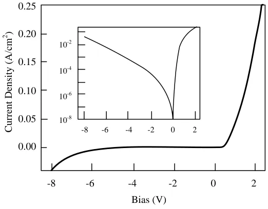
Figure 21. OPD current vs. reverse bias, linear and log scale (inset). Adapted from: [6] © 2009 IEEE
From the log scale in Figure 21, it can be seen that under a reverse bias of 2 V the OPD has a
measurable current density.
Frequency (Hz) N o rm al iz ed G ai n 1 0.8 0.2 0.1 0.6 0.4
[image:31.612.151.412.185.389.2]10 100 1000
Section 1 Page 27 of 113 Charge transport through the 15 nm bathocuproine blocking layer creates an overall low mobility
of carriers, in addition to charge trapping at the surface. This would explain the poor frequency
response seen in Figure 22.
Wavelength (nm)
G
ai
n
400 400 400 1000
10 20 30 40
0
8 V
6 V
4 V
2 V
Figure 23. Photocurrent gain vs. incident wavelength at the voltages indicated. Adapted from: [6] © 2009 IEEE
The spectral response of the OPD is shown in Figure 23 and demonstrates that fabricating
Section 1 Page 28 of 113 E) Organic photodiodes with an amorphous silicon active pixel
Amplifier
Read
Reset
OPD
Pixel
V
CATHV
D_AMPV
G_
R
E
S
E
T
V
D_RESETV
G_READg
mT
RC
FB [image:33.612.169.455.113.404.2]External
Integrator
Figure 24. Schematic representation of the pixel. Adapted from: [7] © 2007 IEEE
Figure 24 shows the pixel setup for experimentation. The dotted rectangle represents the
organic photodiode that is printed on top of the amplifier circuit, allowing for a near 100% fill
factor. Sensitivities for different ratios of widths for the amplifier thin film transistor (TFT) and
Section 1 Page 29 of 113
Zamp/ZRead
0 20 40 60 80 100
0 50 100 150 200 250
300 500/500800/200
600/200 900/100 400/200 300/300 C h ar g e g ai n S ig n al ( li g h t-d ar k ) [p C ]
Light Intensity [µW/cm2]
Figure 25. Signal (light/dark) vs. light intensity. Adapted from: [7] © 2007
Light Intensity [µW/cm2]
S ig n al ( li g h t-d ar k ) [p C ] Active Pixel
0 20 40 60 80 100
0 50 100 150 200 250 300 350 (a)
Light Intensity [µW/cm2]
S ig n al ( li g h t-d ar k ) [p C ]
0 10 20 30 40 50
0 5 10 15 (b) Passive Pixel
Figure 26. (a) OPD with APS 500/500
(b) OPD passive pixel. Adapted from: [7] © 2007 IEEE
Figure 26 demonstrates the improved signal for the APS compared to the passive OPD
setup. This demonstrates that a large-scale OPD APS system could be fabricated to create a
[image:34.612.121.469.306.511.2]Section 1 Page 30 of 113 IV. Conclusion
The CCD array, PPS, and multiple APS pixel setups were explored. It was found that
while the CCD array is an excellent technology for specific applications, it cannot effectively be
used for a large-format sensor due to its dependence on charge transfer. Increasing the distance
between the devices will inevitably degrade their performance. CMOS processes were found to
be more practical for large-format applications. The PPS was explained and compared to
multiple APS systems and found to be inferior. It was demonstrated that using a cascoded
common source amplifier in place of a simpler three-transistor amplifier benefited the system.
Amorphous silicon and organic photodiodes were explored due to their potential applications in
large format systems. While there are OPDs with the desired spectral response, they do not
demonstrate the desired frequency response. Further research using OPDs with column line
amplifiers would be beneficial in proving the plausibility of a printed large-scale image sensor
Section 1 Page 31 of 113 References
[1] © 2007 IEEE. Reprinted, with permission, from El Gamal, A; Eltoukhy, H.;, CMOS image sensors,
Circuits and Devices Magazine, IEEE , May-June 2005
El Gamal, A.; Eltoukhy, H.; , "CMOS image sensors," Circuits and Devices Magazine, IEEE , vol.21, no.3, pp. 6- 20, May-June 2005 doi: 10.1109/MCD.2005.1438751
URL: http://ieeexplore.ieee.org/stamp/stamp.jsp?tp=&arnumber=1438751&isnumber=30986
[2] © 1987 IEEE. Reprinted, with permission, from Wojtczuk, S.; Ballantyne, J.; Wanuga, S.; Chen, Y.; ,
Comparative study of easily integrable photodetectors, Lightwave Technology, IEEE , Oct 1987
Wojtczuk, S.; Ballantyne, J.; Wanuga, S.; Chen, Y.; , "Comparative study of easily integrable photodetectors," Lightwave Technology, Journal of , vol.5, no.10, pp. 1365- 1370, Oct 1987 doi: 10.1109/JLT.1987.1075422
URL: http://ieeexplore.ieee.org/stamp/stamp.jsp?tp=&arnumber=1075422&isnumber=23172
[3] © 2009 IEEE. Reprinted, with permission, from Murari, K.; Etienne-Cummings, R.; Thakor, N.;
Cauwenberghs, G.; , Which Photodiode to Use: A Comparison of CMOS-Compatible Structures, Sensors
Journal, IEEE, July 2009
Murari, K.; Etienne-Cummings, R.; Thakor, N.; Cauwenberghs, G.; , "Which Photodiode to Use: A Comparison of CMOS-Compatible Structures," Sensors Journal, IEEE , vol.9, no.7, pp.752-760, July 2009 doi: 10.1109/JSEN.2009.2021805
URL: http://ieeexplore.ieee.org/stamp/stamp.jsp?tp=&arnumber=4957497&isnumber=4957493
[4] © 1990 IEEE. Reprinted, with permission, from Hayama, M.; , Characteristics of p-i junction amorphous
silicon stripe-type photodiode array and its application to contact image sensor, Electron Devices, IEEE, May 1990
Hayama, M.; , "Characteristics of p-i junction amorphous silicon stripe-type photodiode array and its application to contact image sensor," Electron Devices, IEEE Transactions on , vol.37, no.5, pp.1271-1219, May 1990 doi: 10.1109/16.108189
URL: http://ieeexplore.ieee.org/stamp/stamp.jsp?tp=&arnumber=108189&isnumber=3285
[5] © 2009 IEEE. Reprinted, with permission, from Yang, Y.; Imaoka, H.; Goto, R.; Watanabe, H.; Yamashita,
K.; Miyazaki, M.; Oki, Y.; , Wavelength sensitive organic photo-diodes patterned by ink-jet method, Lasers and Electro-Optics 2009 and the European Quantum Electronics Conference. CLEO Europe - EQEC 2009, IEEE, June 2009
Yang, Y.; Imaoka, H.; Goto, R.; Watanabe, H.; Yamashita, K.; Miyazaki, M.; Oki, Y.; , "Wavelength sensitive organic photo-diodes patterned by ink-jet method," Lasers and Electro-Optics 2009 and the European Quantum Electronics Conference. CLEO Europe - EQEC 2009. European Conference on , vol., no., pp.1, 14-19 June 2009 doi: 10.1109/CLEOE-EQEC.2009.5196479
URL: http://ieeexplore.ieee.org/stamp/stamp.jsp?tp=&arnumber=5196479&isnumber=5191447
[6] Reprinted with permission from Campbell, I. H.; Crone, B. K.; , "A near infrared organic photodiode with gain at low bias voltage," Applied Physics Letters , vol.95, no.26, pp.263302-263302-3, Dec 2009 doi: 10.1063/1.3279133
URL: http://ieeexplore.ieee.org/stamp/stamp.jsp?tp=&arnumber=5372141&isnumber=5372125. Copyright [2009], American Institute of Physics.
Campbell, I. H.; Crone, B. K.; , "A near infrared organic photodiode with gain at low bias voltage," Applied Physics Letters , vol.95, no.26, pp.263302-263302-3, Dec 2009 doi: 10.1063/1.3279133
Section 1 Page 32 of 113
[7] © 2007 IEEE. Reprinted, with permission, from Tedde, S.; Zaus, E.S.; Furst, J.; Henseler, D.; Lugli, P.; ,
Active Pixel Concept Combined With Organic Photodiode for Imaging Devices, Electron Device Letters,
IEEE, Oct 2007
Tedde, S.; Zaus, E.S.; Furst, J.; Henseler, D.; Lugli, P.; , "Active Pixel Concept Combined With Organic Photodiode for Imaging Devices," Electron Device Letters, IEEE , vol.28, no.10, pp.893-895, Oct. 2007 doi: 10.1109/LED.2007.905425
ROCHESTER INSTITUTE OF TECHNOLOGY
Analysis of discrete component implemented pixels
Section 2
Section 2 Page 34 of 113
Abstract – Fabricated CMOS pixels have the advantage over discrete component
implementations in that their passive or active switching networks are fabricated along with the
photodiode in processes designed specifically to optimize the performance of the pixel.
Non-ideal affects such as dark current, parasitic capacitance, and leakage can be mitigated through
process management. Discrete component implementations do not have this customization
advantage and as such will exhibit greater non-ideal effects. In order to better understand the
increased parasitics present, passive and active pixel architectures were implemented and tested.
I. Introduction
Experimental measurements were performed with the Agilent 54622D Mixed Signal
Oscilloscope with 200 MSa/s. Power was provided with the Agilent E3631A Triple Output DC
Power Supply. All waveforms were generated by the Agilent 33250A 80 MHz
Function/Arbitrary Waveform Generator. Resistance measurements were made with the Agilent
34401A Digital Multimeter.
Output Waveform
fc (fs = 200 MHz)
Anti-Alias Filter
f3dB = fsub/100
Sub sample
fsub ~ fc*200
DFT
High-Pass Filter
f3dB = fsub*200
Hamming Window Moving
Average
Figure 1. Sub-sampling and filtering scheme for the Discrete Fourier Transform (M.A. Hopkins, personal
communication)
The processing scheme used for the output data can be seen in Figure 1. In order to
effectively display and process data, output data was sub-sampled with sub-sampling frequency
Section 2 Page 35 of 113 sampled at a rate of 200*fc due to the limitations of the oscilloscope, the sub-sampling block was
omitted.
Before sub-sampling was performed, an anti-aliasing filter that consisted of a first-order
Butterworth low-pass filter with a three dB frequency f3dB = fsub/100.
II. Experimental
A) Light Emitting Diode (LED) control and response
The light impinging on the surface of the photodiode of interest in all pixel configurations
was modulated with an LED. It is important to consider the response of the LED as a function of
frequency as any deviation from the desired response will appear in the measurement of the pixel
and skew the results. For all experiments the QED223 Plastic Infrared LED produced by
Fairchild Semiconductor is used (peak wavelength of 890 nm, maximum forward current of 150
mA).
i) Voltage-controlled LED, op-amp configuration
+
V
sig+
V
DDOpa
V
LED+
Figure 2. Voltage-controlled LED
Figure 2 shows the schematic where a square wave signal Vsig was applied to the positive
Section 2 Page 36 of 113 output of the op-amp are tied to the anode of the LED. This forced the anode of the LED to be
driven to the voltage applied by the signal generator. The voltage VLED was then measured as the
signal center frequency was swept from 1 kHz to 5 MHz with a square wave that had a
peak-to-peak voltage of 1.4 V and a DC offset of 0.7 V.
[image:41.612.103.523.179.567.2]Figure 3. DFT of VLED where fc of Vsig equals 1 kHz
Figure 4. DFT of VLED where fc of Vsig equals 34 kHz
1 kHz applied signal
Section 2 Page 37 of 113
Figure 5. DFT of VLED where fc of Vsig equals 100 kHz
For Figures 3-5 the DFTs were normalized by dividing all subsequent frequencies by the
magnitude of the first harmonic of the applied square wave fc = 1 kHz. By normalizing all the
frequencies by this magnitude, the loss of signal can be observed in all of the harmonics.
∑ (1)
Equation (1) is the Fourier expansion of an ideal square wave. From (1) it can be seen that the
desired frequency harmonics are fc* (2k + 1) where k is an integer value from 0 to infinity. All
other emergent harmonics are considered distortion, as they do not contribute to the formation of
a square wave.
From Figure 3, there were no observable even-order harmonics, and the odd-order
harmonics decay as expected. This is due to the low fc of 1 kHz. In Figures 4 and 5, the
emergence of even-order harmonics was observed. By increasing fc from 34 kHz to 100 kHz, the
Section 2 Page 38 of 113
Figure 6: Frequency sweep of Vsig with fc and the emerging harmonics in VLED
Figure 6 concatenates the resultant harmonics in VLED for each of the frequencies tested.
While the three-dimensional representation of the harmonics demonstrates the loss of the
primary harmonic at fc at roughly 100 kHz, the magnitude of undesired even-order harmonics is
obscured by the desired odd-order harmonics.
Anti-Alias Filter f3dB = fsub/100
Anti-Alias Filter f3dB = fsub/100
Output Waveform fc (fs= 200 MHz)
Ideal Waveform fc (fs = 200 MHz)
Sub sample fsub ~ fc*200
Sub sample fsub ~ fc*200
DFT DFT
DFT DFT
DFT DFT THD High Pass Filterf3dB = fsub*200
High Pass Filter f3dB = fsub*200
Hamming Window Hamming Window ∑RHD Moving Average Moving Average
Section 2 Page 39 of 113
f
sub~ 200*f
c [image:44.612.107.494.75.292.2]f
sub< 200*f
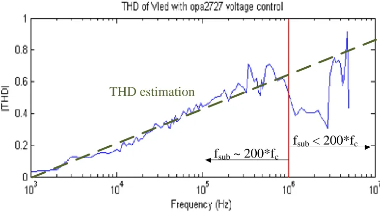
cTHD estimation
Figure 8. Total Harmonic Distortion (THD) of VLED
Figure 7 illustrates the processing scheme that was implemented for each frequency’s
THD calculation, where RHD is the Resultant Harmonic Distortion that emerges from the
absolute value of the subtraction of the ideal harmonics from the non-ideal output harmonics.
Figure 8 shows the THD that results from the calculation shown in Figure 7 as a function of
frequency. It is important to consider for all frequency analysis purposes that the oscilloscope’s
sampling frequency is limited to 200 MHz. It is therefore impossible for the sub-sampling
frequency to maintain the 200*fc sub-sampling frequency for all center frequencies above 1
MHz. As a result the accuracy of all frequency analysis decreases with an increase in fc above 1
MHz. An approximation was made based on the trend of the data to predict the THD for
frequencies above fc = 1 MHz.
From Figure 8 it can be seen that the THD generally trends upwards with an increase in
frequency. Distortion is a direct result of parasitic capacitances present in the circuit and the
limitations in the op-amp’s ability to reproduce high-frequency harmonics with the desired gain.
Section 2 Page 40 of 113 THD directly correlates to a more square-like wave which in turn, would increase the efficacy of
sampling schemes such as Correlated Double Samplings (CDS).
ii) Current-controlled LED
+
V
sig+
V
DDOpa
V
sig’+
RFigure 9. Current-controlled LED (R.J. Bowman, personal communication)
Figure 9 shows the schematic where a square wave signal Vsig was applied to the positive
input of an OPA2727 operational amplifier made by Texas Instruments. The output of the
op-amp was tied to the gate of a discrete BSS123 NMOS transistor produced by Infineon and the
negative input of the op-amp was tied to a 10 Ω resistor. This forces the voltage Vsig to form
across the resistor which has a linear relationship with the current through the LED. The voltage
Vsig’ was then measured as the signal center frequency was swept from 1 kHz to 5 MHz with a
Section 2 Page 41 of 113
Figure 10. DFT of Vsig’ where fc of Vsig equals 1 kHz
[image:46.612.95.502.64.660.2]Figure 11. DFT of Vsig’ where fc of Vsig equals 34 kHz
Figure 12. DFT of Vsig’ where fc of Vsig equals 100 kHz
1 kHz applied signal
34 kHz applied signal
Section 2 Page 42 of 113
Figure 13. DFT of Vsig’ where fc of Vsig equals 220 kHz
Similar to the analysis of the voltage-controlled LED in Figure 2, the DFTs are
normalized by dividing all subsequent frequencies by the magnitude of the first harmonic of the
applied square wave fc = 1 kHz.
From Figure 10, there were no observable even-order harmonics, similar to Figure 3.
Unlike the voltage-controlled circuit in Figure 2, the current-controlled circuit in Figure 9 does
not show significant even-order harmonics until fc = 220 kHz, as seen from Figures 10-13.
Figure 14: Frequency sweep of Vsig with fc and the emerging harmonics in Vsig’
Section 2 Page 43 of 113 Figure 14 concatenates the resultant harmonics in Vsig’ for each of the frequencies tested.
Similarly to Figure 13, Figure 14 demonstrates the loss of power in the primary harmonic at 220
kHz.
f
sub~ 200*f
cf
sub< 200*f
c [image:48.612.109.530.185.396.2]THD estimation
Figure 15. Total Harmonic Distortion (THD) of Vsig’
Figure 15 illustrates the THD for the current-controlled LED as a function of frequency.
The same processing scheme shown in Figure 7 was used to calculate the THD. Frequencies <
220 kHz have a THD < 40%, a significantly higher fc than was observed with the
voltage-controlled LED configuration.
iii) Voltage-controlled LED vs. current-controlled LED
Ultimately, the goal of applying a square wave signal to the LED for either voltage or
current control is to produce a square-like light intensity.
(
) (2)
Section 2 Page 44 of 113 where Isis the saturation current, Vsig is the applied voltage, n is the ideality factor, VT is the
threshold voltage, K is a group of constants, and I is the current through the LED. By substituting
(2) into (3) and substituting Vsig with ∆V, the error in luminosity can be calculated as a function
of an error voltage.
( ) (4)
(5)
From (4) and (5) it can be seen that an error in the applied voltage will result in an
exponential error in luminosity and an error in current will produce a linear error in luminosity.
In addition to the decreased error in the THD analysis, the current-controlled method is clearly
superior to the voltage-controlled method. By improving the control method for the LED, the
performance of the implemented pixels should show an improvement. In order to simplify the
analysis of the pixels, the LED will be considered a part of the system, and the output of the
pixels will not be adjusted to compensate for the non-ideal light source.
Vout + +
Vsig +
VDD
Opa
VDD
Vout + +
Vsig +
Opa
R
(a) (b)
Section 2 Page 45 of 113
[image:50.612.101.497.89.478.2]Figure 17. THD for voltage-controlled LED with a passive pixel setup
Figure 18. THD for current-controlled LED with a passive pixel setup
Figure 16 (a) and (b) illustrate the circuit setup used for comparing the voltage- and
current-controlled configurations of the LED. Figure 17 and 18 show the analysis of the THD for
the passive pixel for the voltage- and current-controlled LED configurations, respectively. It can
be seen that the current-controlled method results in a THD of 50.67% at 100 kHz while the
voltage-controlled method has a THD of 60.31% at the same center frequency. As expected, the
current-controlled method for the LED provides a more square-like luminosity than the
voltage-controlled method. As a result, all further experiments will implement the current-voltage-controlled
Section 2 Page 46 of 113 B) Passive Pixel
Using the configuration in Figure 16 (b) the center frequency fc was swept from 1 kHz to
5 MHz with a square wave current pulse with a low output of 0.2 mA and a high output of 32
mA. The passive pixel puts the photodiode under a reverse bias of 5 V and incident light
modulates the current through the photodiode where it is measured as an output voltage across
[image:51.612.100.500.232.590.2]the 1 kΩ resistor.
Figure 19. DFT of Vout where fc of Vsig equals 1 kHz
Figure 20. DFT of Vout where fc of Vsig equals 34 kHz
1 kHz applied signal
Section 2 Page 47 of 113
Figure 21. DFT of Vout where fc of Vsig equals 100 kHz
For Figures 19-21 the response was normalized by the primary harmonic of the 1 kHz
response. It can be seen that the even-order harmonics for the passive pixel do not start to emerge
until fc ~ 100 kHz. This shows that the passive pixel setup has a reasonably linear response.
Figure 22. Frequency sweep of Vsigwith fc and the emerging harmonics in Vout
Figure 22 concatenates the resultant harmonics in Vout for each of the frequencies tested. There is
Section 2 Page 48 of 113
Figure 23. THD of Vout for the passive pixel
The signal loss observable in Figure 22 and the distortion observed in Figure 23 for the
passive pixel are likely due to the RC time constant of the pixel. Section 1 of this paper
elucidated the nature of parasitic capacitances in passive pixel systems and their effect on the
performance of the pixel. In order to increase the frequency range where one would be able to
comfortably operate this device, either the parasitic capacitance or the resistance would have to
be decreased. While the load resistance is controllable, the capacitance of the discrete diode is
not. Any decrease in the R would correlate to a decrease in Vout, which would improve the
linearity and frequency response of the device, but it would also make the signal harder to
Section 2 Page 49 of 113 C) Active Pixel Vbias = 0 V
+
Vsig
+
VDD
Opa
+
OpaRf
VDD
R
Vout
Vbias
Figure 24. Schematic for the Active Pixel configuration
Figure 24 shows the circuit implemented for the active pixel configuration where R =
10 Ω and Rf = 1 kΩ. The voltage Vbias may be increased in order to improve the frequency
response of the circuit by thinning the depletion region within the photodiode. Similar to the
cascode amplified active pixel reviewed in Section 1, the opa2727 used here serves to partially
decouple the photodiode from its own capacitance, allowing for larger resistance values and
higher gain in the system without compromising the frequency response.
Figure 25. DFT of Vout where fc of Vsig equals 1 kHz
Section 2 Page 50 of 113
Figure 26. DFT of Vout where fc of Vsig equals 34 kHz
Figure 27. DFT of Vout where fc of Vsig equals 100 kHz
For Figures 25-27 the response was normalized by the primary harmonic of the 1 kHz
response. It can be seen that the even-order harmonics start to emerge at fc ~ 34 kHz, unlike the
passive pixel configuration where the even-order harmonics emerged at fc ~ 100 kHz. Further,
the primary harmonic in Figure 27 shows significant power loss at fc ~ 100 kHz unlike Figure 21. 34 kHz applied signal
Section 2 Page 51 of 113
Figure 28. Frequency sweep of Vsig with fc and the emerging harmonics in Vout
Figure 28 concatenates the resultant harmonics in Voutfor each of the frequencies tested.
There is a significant loss of response and linearity in Vout for all frequencies above fc ~ 34 kHz.
Figure 30. THD of Vout for the active pixel with Vbias = 0 V
The signal distortion seen in Figure 30 is significantly greater than in Figure 23. At fc=
34 kHz the passive pixel system has THD = 42.82% while the active system has 54.31%. As the
frequency of fc increases, the difference between the THDs shrinks. At fc = 260 kHz the passive
system has THD = 71.96% and the active system has THD = 81.61%. Eventually, the THD of
the passive system peaks at 100% for fc = 950 kHz, while the active system has THD = 62%. The
reason for this behavior is likely due to the decoupling effect the amplifier has on the photodiode
capacitance, allowing the system to maintain its output as long as the amplifier can provide the
Section 2 Page 52 of 113 does not explore the increased potential of the active system to provide the same frequency
response characteristics with an increased Rf unlike the passive pixel system, which is limited by
its RC time constant.
D) Active Pixel Vbias = 1 V
Figure 24 shows the circuit implemented for the active pixel configuration where R =
10 Ω and Rf = 1 kΩ.
[image:57.612.101.505.255.630.2]Figure 31. DFT of Vout where fc of Vsig equals 1kHz
Figure 32. DFT of Vout where fc of Vsig equals 34 kHz
1 kHz applied signal
Section 2 Page 53 of 113
Figure 33. DFT of Vout where fc of Vsig equals 100 kHz
For Figures 31-33 the response was normalized by the primary harmonic of the 1 kHz
response. It can be seen from these figures that even-order harmonics do not start to emerge in
the system until fc ~ 100 kHz.
Figure 34. Frequency sweep of Vsig with fc and the emerging harmonics in Vout
Figure 34 concatenates the resultant harmonics in Vout for each of the frequencies tested.
The frequency response for the active pixel with 1 V of bias significantly outperforms the 0 V
Section 2 Page 54 of 113
Figure 35. THD of Vout for the active pixel with Vbias = 1 V
The signal distortion seen in Figure 35 is comparable to the passive pixel THD in Figure
23. At fc= 34 kHz the passive pixel system has THD = 42.82% while the active system with Vbias
= 1 V has 42.45%. As the frequency of fc increases, the difference between the THDs increases.
At fc = 260 kHz the passive system has THD = 71.96% and the active system has THD =
67.87%. With the addition of just 1 V of bias, the active system surpasses the passive system and
still has the potential to increase the system gain without negatively impacting the frequency
Section 2 Page 55 of 113 E) Active Pixel Vbias = 2 V
Figure 24 shows the circuit implemented for the active pixel configuration where R =
10 Ω and Rf = 1 kΩ.
[image:60.612.101.502.148.525.2]Figure 36. DFT of Vout where fc of Vsig equals 1 kHz
Figure 37. DFT of Vout where fc of Vsig equals 34 kHz
1 kHz applied signal
Section 2 Page 56 of 113
Figure 38. DFT of Vout where fc of Vsig equals 100 kHz
For Figures 36-38 the response was normalized by the primary harmonic of the 1 kHz
response. It can be seen from these figures that even-order harmonics do not start to emerge in
the system until fc ~ 100 kHz, and there is a slight improvement in the number of odd-order
harmonics present in Figure 38 when compared to Figure 33.
Figure 39. Frequency sweep of Vsig with fc and the emerging harmonics in Vout
Figure 39 concatenates the resultant harmonics in Vout for each of the frequencies tested.
The frequency response for the active pixel with 2 V of bias slightly outperforms the active pixel
Section 2 Page 57 of 113
Figure 40. THD of Voutfor the active pixel with Vbias = 2 V
The signal distortion seen in Figure 40 is comparable to the active pixel THD in Figure
35. At fc= 34 kHz the active pixel system with Vbias = 1 V has THD = 42.45% while the active
system with Vbias = 2 V has 37.87%. At fc = 260 kHz the active system with Vbias = 1 V has THD
= 67.87% and the active system with Vbias = 2 V has THD = 64.82%. By increasing the bias
applied to the photodiode, the response of the pixel is improved. While increasing the bias of the
photodiode improves the pixel performance, it could potentially also decrease the available
Section 2 Page 58 of 113 F) Active Pixel Vbias = 3 V
Figure 24 shows the circuit implemented for the active pixel configuration where R =
10 Ω and Rf = 1 kΩ.
Figure 41. DFT of Vout where fc of Vsig equals 1 kHz
Figure 42. DFT of Vout where fc of Vsig equals 34 kHz
1 kHz applied signal
Section 2 Page 59 of 113
Figure 43. DFT of Vout where fc of Vsig equals 100 kHz
For Figures 41-43 the response was normalized by the primary harmonic of the 1 kHz
response. Similar to the 1 V and 2 V biases, even-order harmonics do not start to emerge in the
system until fc ~ 100 kHz and there is a slight improvement in the magnitude of the odd-order
harmonics in Figure 43 over the odd-order harmonics in Figure 38.
Figure 44. Frequency sweep of Vsig with fc and the emerging harmonics in Vout
Figure 44 concatenates the resultant harmonics in Vout for each of the frequencies tested.
Section 2 Page 60 of 113
Figure 45. THD of Voutfor the active pixel with Vbias = 3 V
The signal distortion seen in Figure 45 is comparable to the active pixel THD in Figure
40. At fc= 34 kHz the active pixel system with Vbias = 2 V has THD = 37.87% while the active
system with Vbias = 3 V has 33.93%. At fc = 260 kHz the active system with Vbias = 2 V has THD
= 64.82% and the active system with Vbias = 3 V has THD = 62.91%. The further-increased bias
slightly improves the pixel performance, but it appears to have a diminishing return.
G) Passive Pixel, RL = 10 kΩ, Iled = 0.2 – 3.8 mA
Using the configuration in Figure 16 (b), the center frequency fc was swept from 1 kHz to
5 MHz with a square wave current pulse with a low output of 0.2 mA and a high output of 3.8
mA. The passive pixel puts the photodiode under a reverse bias of 5 V and incident light
modulates the current through the photodiode where it is measured as an output voltage across
the 10 kΩ resistor. The new high-level current was set such that Vout ~ 1.56 V. The decreased
Section 2 Page 61 of 113
Figure 46. DFT of Vout where fc of Vsig equals 1 kHz
[image:66.612.101.500.68.638.2]Figure 47. DFT of Vout where fc of Vsig equals 34 kHz
Figure 48. DFT of Vout where fc of Vsig equals 100 kHz
1 kHz applied signal
34 kHz applied signal
100 kHz applied signal
Section 2 Page 62 of 113 For Figures 46-48 the response was normalized by the primary harmonic of the 1 kHz
response. It can be seen that the even-order harmonics for the passive pixel do not start to emerge
until fc ~ 100 kHz.
Figure 49. Frequency sweep of Vsig with fc and the emerging harmonics in Vout
Figure 49 concatenates the resultant harmonics in Vout for each of the frequencies tested.
The frequency response for the increased load resistance shows more power loss in the primary
harmonic than seen in Figure 22 (1 kΩ load passive).
Figure 50. THD of Voutfor the passive pixel
The signal distortion seen in Figure 50 is significantly greater than in Figure 23. At fc=
34 kHz the passive pixel system with RL = 1 kΩ has THD = 42.82% while the same system with
Section 2 Page 63 of 113 71.96% and with RL = 10 kΩ the THD = 100%. As expected, the THD for the passive pixel
system shows a significant degradation in the signal quality with the increase in resistance due to
the increased RC time constant.
H) Passive Pixel, RL = 10 kΩ, Iled = 0.2 – 32 mA
Using the configuration in Figure 16 (b) the center frequency fc was swept from 1 kHz to
5 MHz with a square wave current pulse with a low output of 0.2 mA and a high output of 32
mA. The passive pixel puts the photodiode under a reverse bias of 5 V and incident light
modulates the current through the photodiode where it is measured as an output voltage across
the 10 kΩ resistor. In order to preserve the Vout ~ 1.56 V the LED’s position was adjusted so that
the light incident on the surface of the photodiode was decreased to the point where Vout ~ 1.56
V. By keeping the LED under a higher bias current the LED should exhibit better high-frequency
response characteristics, and the configuration is more representative of what would be seen in
an imaging device with this configuration.
Figure 51. DFT of Vout where fc of Vsig equals 1 kHz
1 kHz applied signal
Section 2 Page 64 of 113
Figure 52. DFT of Vout where fc of Vsig equals 34 kHz
Figure 53. DFT of Vout where fc of Vsig equals 100 kHz
For Figures 51-53 the response was normalized by the primary harmonic of the 1 kHz
response. It can be seen that the even-order harmonics for the passive pixel do not start to emerge
until fc ~ 100 kHz.
34 kHz applied signal
Section 2 Page 65 of 113
Figure 54. Frequency sweep of Vsig with fc and the emerging harmonics in Vout
Figure 54 concatenates the resultant harmonics in Vout for each of the frequencies tested.
The frequency response for the increased load resistance shows more power loss in the primary
harmonic than seen in Figure 22 (1 kΩ load), but less than seen in Figure 49 (10 kΩ load,
p