International Journal of Innovative Technology and Exploring Engineering (IJITEE) ISSN: 2278-3075,Volume-8, Issue-9S4, July 2019
Abstract: Continuous increase in the demand of electricity around the globe has created a great interest in the renewable energy sources. In the recent years Photo Voltaic (PV) power generation has emerged out to be a considerable solution to world energy crisis. The major problem encountered in the implementation of PV is its low voltage output. This study proposes a converter having capability of high voltage boost. The proposed converter utilizes switched capacitors and switched inductors to uplift the output voltage of dc-dc converter. The proposed topology also offers a bonus of reduces voltage stress on the circuit components and thus improved reliability. MATLAB Simulation and the derived results display an improved voltage gain reduced stress. The simulation model also includes PV module to examine converter’s adaptability with PV module.
Index Terms: Quasi Z-Source, dc-dc converter, Voltage gain, PV.
I. INTRODUCTION
In the recent days the conflict between the energy requirement and the fossil fuel supply has been a concern for human development. This in turn has made the renewable energy sources the need of the hour and a popular energy source. Photovoltaic (PV) has emerged as a significant contributor in the world’s energy collection because it is clean, emission-free, and has high reliability [1].
One of the biggest hurdle in the way of using the solar energy is the low output voltage of the PV arrays. The conventional bridge structures boost converters are found to have following inherited shortcomings in case of Voltage fed converters [20]
Both switches of a single phase leg cannot be gated simultaneously. Else, a shoot-through would take place and damage the switches which adversely effects the converter’s reliability.
An additional snubber circuit, required to prevent the voltage overshoot in secondary rectifier diode may reduce efficiency of the converter and reliability of the system.
Similarly the current source fed full bridge converter exhibits the following limitations
In any case one of the upper group switches and one of the lower group switches has to be gated ON and maintained ON at any instant else the dc inductor will be open circuited and will destroy the devices. It is a major issue
Revised Manuscript Received on July 10, 2019.
Mr.Manish Sharma, Department of Electrical Engineering, Poornima Institute of Engineering and Technology, Jaipur, India.
Mr. Prakash Bahrani, Department of Electrical Engineering, Aravali Institute of Technical Studies, Udaipur, India.
while speaking of reliability.
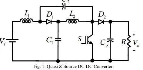
[image:1.595.306.542.316.432.2]Because of above mentioned limitations a new topology of DC-DC converters came into picture and generally known as Z- Source converters [3]. When the ZSC is used for boost action it displays several disadvantages such as the discontinuous input current and high voltage stress on the capacitor[21]. In order to eliminate the disadvantages of the ZSC a new circuit topology with modified structure of the ZS, known as Quasi Z-Source was introduced. Basic structure of a conventional QZS based dc-dc converter is shown in Fig. 1.
Fig. 1. Quasi Z-Source DC-DC Converter
The QZS based DC-DC converter offers several advantages such as high reliability and higher voltage gain then the traditional ZS DC-DC converter at less number of elements. But it still suffers from a disadvantage of low voltage gain. A lot of research has taken place to improve the voltage gain of the QZS based converters. [36]-[37] proposed use of coupled inductors for the purpose of improvement of voltage gain of the QZS based DC-DC converter. Use of cascaded QZS converters was proposed in [38]-[42] but use of multiple stages provides improved voltage gain at a cost of remarkable increased number of components. Due to this high power loss, low efficiency, low reliability was noticed. Hence, this method is also not found to be a suitable and optimized solution.
[44] proposed use of switched inductors. This topology used one inductor and three diodes along with the traditional QZS DC-DC converter. The proposed topology could obtain high voltage gain but involved limitations like restricted duty cycle and amplified voltage stress on the diodes and switches. In line of the same use of switched capacitors was suggested in [45] but the issues found with switched inductors still remained.
This paper presents a novel QZS based dc-dc converter that is equipped with a combination of switched inductors and capacitors to achieve a
high voltage gain.
A Novel Quasi Z-Source based DC-DC
Converter with High Voltage Gain in Photo
Voltaic applications
II. A NOVEL QZS BASED DC-DC CONVERTER Quasi Z-Source (QZS) converter shown in fig. 1 has been suggested to be the most useful converter to serve the above mentioned purpose. Though it is suitable for variety of applications but still has a limitation of low voltage gain and difficult to employ in high voltage applications.
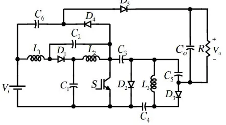
[image:2.595.54.285.181.309.2]In this study we propose a new circuit topology to achieve high boost QZS DC-DC converter. As shown in fig. 2, in this topology four switched capacitors and one switched inductor are also used to increase the boost capability of the converter.
Fig. 2. A novel high voltage gain QZS DC-DC converter The operation of the novel converter includes three operating modes. The general relation for the duty cycle of the switch stands like:
(1)
[image:2.595.54.284.505.625.2]The on time of the switch is then stand equal to DT and the off time is given by . A. Mode I ( ) Fig. 3 displays equivalent circuit of the novel converter in mode I. Here, charging of L1 and L2 takes place by C1 and C2 and L3 is charged by Capacitor C3 and the load. Therefore, the inductors L1, L2 and L3, and the capacitor C4 get charged. Whereas, the voltages across C1, C2, C3, C5 and C6 get discharged. Fig. 3. Equivalent circuit of the proposed converter for mode I Through the application of the KVL following relations can be drawn for mode I operation of the novel converter. (2)
(3)
(4)
(5)
B. Mode II ( ) The 2nd mode of operation begins when the switch is turned off. In this mode, D1, D3 and D4 are forward biased, while, D2 and D5 are reverse biased. The duty cycle of the mode II is symbolized by D´. In this mode, the capacitors C1, C2, and C3 get charged through inductors L1 and L2. C6 is also charged through the path provided by D4. Simultaneously the inductor L3 and capacitor C4 charge the capacitor C5. Consequently, the capacitors C1, C2, C3, C5 and C6 get charged, while, the capacitor C4 and the inductors L1, L2, and L3 are discharged. By applying KVL to Mode II the following relationships can be deduced (6)
(7)
(8)
(9)
(10)
C. Mode III ( ) As indicated in mode II of the operation of the novel converter the voltage across the capacitor C4 falls and the voltage across capacitor C5 rises. As equates , D2 gets forward biased and starts conducting. Mode III of the operation begins with conduction of D2. In this mode, the switch is still remains off, D1, D3 and D4 are forward biased, and D2 and D5 are reverse biased. During this mode, capacitors C3 and C5 are charged through L1 and L2 and also capacitor C6 is charged over the path provided by D4. Amidst this, due to the conduction of D2, the capacitors C4 and C5 forms parallel connection and are charged through L3. Consequently, the capacitors C1, C2, C3, C4, C5 and C6 get discharged and the inductors L1, L2 and L3 get charged. following relation can also be found true for mode III (11)
D. Steady State Analysis The voltage balance law for inductor L1 gives the following relation (12)
Similarly, application of Voltage balance law for inductor L2 gives (13)
By substituting vC2 from (13) into (12) VC1 and VC2 in the steady state can be written as (14)
(15)
When the voltage balance law is applied to inductor L1 using equation (2) and (7) the following expression can be formed (16)
By replacing the value of VC2 in equation (16) from equation (15) gives (17) Through the application of voltage balance law for inductor L3 from the equations (5) and (10) gives the
International Journal of Innovative Technology and Exploring Engineering (IJITEE) ISSN: 2278-3075,Volume-8, Issue-9S4, July 2019
(18)
Replacement of VC6 from (17) to (18) gives that (19) Application of voltage balance law for inductor L2 using (4) and (8) gives the following relation (20)
Replacing VC1 and ( ) from (14) and (19) respectively into the above relation gives expression for VC5 as follows (21)
Now, when voltage balance law is applied for L3 using (5) and (10) the following expression can be derived (22)
Substitution of values from (17) and (19) into above relationship gives (23)
(24)
Application of voltage balance law for L1 from (3) and (6) gives the following expression (25)
While we replace all steady state capacitor voltages in above expression from (14), (15), (17), (21), (23) and (24) it gives the relation for voltage gain as (26)
The general relation for an inductor on a switching period is given by (27)
Replacing the values of capacitor voltages in the equations of inductor voltages gives the following relation (28)
(29)
Using the values of VL1, VL2, and VL3 in equation (27) gives us the following expressions (30)
(31)
is an indication of ripple current which is 10% of the input current for L1 and L2 and 50% of the output current for L3 gives the following relations (33)
(34)
Similarly, a general relation for a capacitor over a switching period is given by (35)
In above equation is the ripple voltage for the capacitor and considered to be 2% of the voltage across capacitor. As the voltages across C1, C2, C3, C4, C5 and C6 has already been calculated and the voltage across Co is equal to Vo, the capacitor values can be obtained as (36)
(37)
(38)
(39)
(40)
III. MATLAB/SIMULINK MODEL OF THE PROPOSED CONVERTER WITH CONSTANT DC
SOURCE AND PHOTO VOLTAIC ARRAY All the simulations are performed in MATLAB Simulink version R2016a.
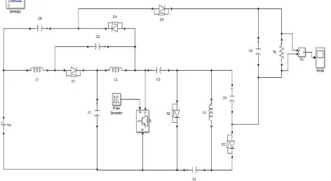
A. Simulation of basic structure of the proposed novel QZS based DC-DC converter with constant DC source
Fig. 4. shows simulation model for the proposed converter. The simulation parameters are shown in table 1.
TABLE I. Parameters used for simulation
Input Voltage (Vin)
C1& C2 C3, C4, C5, C6& C0 L1, L2& L3 RL
100 V 330 µF 100 µF 3 mH 500 Ω
As shown in Fig 4 a DC voltage of 100 Volt is applied to the proposed converter structure. The converter includes 3 inductor of 3 mH and 6 capacitors to derive the proposed topology. The inductor L1& L2 and capacitors C1& C2 forms
the Z-Source circuit. While the inductor L3 and capacitors
C3, C4, C5 & C6 are used as switched inductors and switched
capacitors. A resistive load of 500 Ω is used to collect the output. A capacitor C0 is connected across the load to make
the output voltage stable.
[image:3.595.309.545.561.690.2]The switch used hereby is an Insulated Gate Bipolar Transistor (IGBT) controlled through the gate signal provided by a pulse generator having a switching frequency of 40 KHz. The system also includes five diodes for switching the inductors and capacitors.
B. Simulation Model of the proposed converter with Photo Voltaic array
In order to examine the feasibility of the proposed converter with PV application another simulation is performed in the same Simulink environment by connecting the proposed converter with a PV array.
The PV array used for the simulation is the ‘Soltech 1STH-350-WH’ with two series connected strings.
[image:4.595.299.556.48.153.2]A capacitor of 100 µF is connected across the PV array to maintain constant output voltage from the array. The simulation model of the proposed converter connected to a PV array has been displayed in Fig 5. The PV array was supplied with a constant irradiation of 1000 W/m2 and temperature of 25° C.
[image:4.595.307.552.220.363.2]Fig. 5. Simulation model of the proposed converter with PV array
Fig. 6. Simulation model of the conventional Quasi Z-Source based DC-DC converter
Table II. Maximum Power Point parameters of the PV array
S. N. Irradiation
(W/m2) Temp. (° C) P(Watts) MPP I(Amp.) MPP V(volts) MPP
1 1000 25 700 9.4 86
2 1000 35 675 8.2 82.1
3 1000 45 650 8.3 78.4
C. Variants of input for verification of results
The operation of proposed converter is verified by applying different variants of input to the converter. Table III shows the details of variants applied to the PV module used to supply the input voltage to the converter. The duty cycle is also varied to verify the expression of voltage gain derived in equation (26)
Table III. Variants of supply for PV module
Sr. N. Irradiation Temperature Duty Cycle
(W/m2) (° C)
1 1000 25 0.43
2 1000 35 0.43
3 1000 45 0.43
4 500 25 0.35
5 500 35 0.35
6 500 45 0.35
7 250 25 0.30
8 250 35 0.30
9 250 45 0.30
IV. RESULTS OF SIMULATION AND DISCUSSION OF RESULTS
[image:4.595.52.289.239.380.2]A. Simulation results obtained by connecting the proposed converter with the dc voltage source
[image:4.595.47.288.423.564.2]Fig. 7. Output voltage of the proposed converter with dc voltage source As displayed in the results of Fig. 7 the output voltage received against the input voltage of 100 Volts is around 1500 Volts. According to the expression derived for voltage gain in equation (26) the voltage gain for a duty cycle of 0.43 should fall around the similar range as found in the simulation results. Furthermore, it is also notable that the output voltage obtained after the proposed converter is smooth enough for being accepted in all kinds of industrial applications and contains allowable ripples.
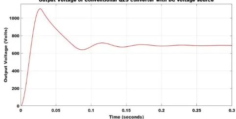
Fig. 8. Output Voltage of the conventional converter with dc voltage source
[image:4.595.309.550.484.606.2]International Journal of Innovative Technology and Exploring Engineering (IJITEE) ISSN: 2278-3075,Volume-8, Issue-9S4, July 2019 It can be noticed that the voltage output of the
conventional converter is quite low as compared to the voltage output of 1500 Volts received with the proposed converter while operated at similar duty cycle of the switch and supplied with same input voltage of 100 Volts. If can also be noticed from the two waveforms that the output voltage obtained with the proposed converter is smoother than the output voltage obtained with the conventional converter.
Fig. 09 show the voltage gain versus duty cycle graph for the proposed converter. As shown in the Fig. 09 the proposed converter displays a smooth relationship between duty cycle and the converter voltage gain. It has also been indicated by the above graph that the proposed converter offers a very high voltage gain and the duty cycle is not limited. The duty cycle of the converter can be varied up to 0.5 and boost action can be maintained.
Fig. 09. Relation between the voltage gain and the duty cycle for proposed converter
It can also be noticed from the graph that the slop of the curve is also mild. The aforementioned observation can lead us to the conclusion that a very high voltage gain can be achieved with the proposed converter with the sage distance from Dmax.
B. Comparison between input and output voltage of the proposed converter for variety of inputs for PV module
[image:5.595.311.546.89.219.2]In line of the same further simulations were performed with a PV module to check the feasibility of the proposed converters with renewable energy sources.
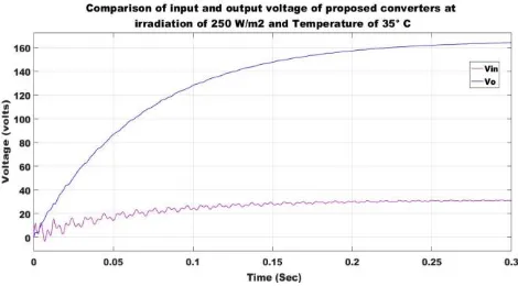
Fig. 10. Comparison of input and output voltage of the proposed converter at Irradiation of 250 W/m2 and 25° C Temperature
As shown in Fig. 10 the output voltage received at the irradiation of 250 W/m2 and 25° C temperature the output voltage received is 162.4 Volts against the input voltage of 30.9 Volts.
Similarly, the output voltage received at the irradiation input of 250 W/m2 and 35° C temperature is 164.1 Volts against the input voltage of 31 Volts and the output voltage was having less harmonics. The waveforms obtained for
input and out voltage are shown in Fig. 11 clearly displays the uniformity of the output voltage as compared to the input supplied to the converter circuit.
Fig. 11 Comparison of input and output voltage of the proposed converter at Irradiation of 250 W/m2 and 35° C Temperature
Fig. 12 shows the output voltage and input voltage waveforms for irradiation input of 250 W/m2 and 45° C temperature. The output voltage received is 165.7 Volts against the input voltage of 31.5 Volts.
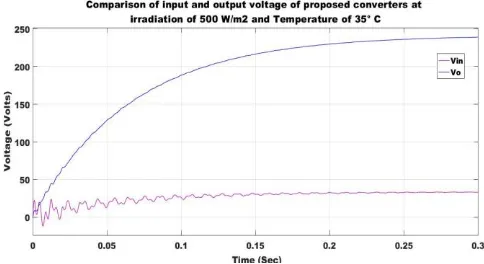
Fig. 13 gives the input and output voltage at the input of 500 W/m2 irradiation and 25° C temperature. The output voltage is observed to be at the level of 237 Volts for the input voltage of 33 Volts.
[image:5.595.52.290.254.389.2]The output voltage received at the input of 500 W/m2 irradiation and 35° C temperature is 239 Volts while the input voltage is at 33 Volts. The waveforms are shown in Fig. 14. As shown in the figure the output voltage is still smoother than the input voltage.
[image:5.595.309.546.410.544.2]Fig. 12. Comparison of input and output voltage of the proposed converter at Irradiation of 250 W/m2 and 45° C Temperature
[image:5.595.308.550.498.682.2] [image:5.595.55.286.540.683.2]Fig. 14. Comparison of input and output voltage of the proposed converter at Irradiation of 500 W/m2 and 35° C Temperature
For the input irradiation of 500 W/m2 and 45° C temperature the output voltage is 241.2 Volts against the input voltage of 33.5 Volts. The input and output voltage waveforms are shown in the Fig. 15.
Fig. 16 displays the input and output voltage for the input of 1000 W/m2 irradiation and 25° C temperature. The output voltage is found to be 217.25 Volts while the input voltage is 16 Volts. The voltage gain shows significant improvement at the duty cycle of 0.43.
The output voltage is 219.2 Volts against the input voltage of 16 Volts for the input irradiation of 1000 W/m2 and temperature of 35° C. The input and output voltage waveforms are shown in Fig. 17.
[image:6.595.309.552.62.210.2]Finally the PV module is supplied with irradiation of 1000 W/m2 and temperature of 45° C. The input voltage applied to the converter is 16.1 Volts and the output voltage obtained from the converter is 221.1 Volts. The input and output voltage are displayed in Fig. 18.
[image:6.595.306.550.268.400.2]Fig. 15. Comparison of input and output voltage of the proposed converter at Irradiation of 500 W/m2 and 45° C Temperature
Fig. 16. Comparison of input and output voltage of the proposed converter at Irradiation of 1000 W/m2 and 25° C Temperature
Fig. 17. Comparison of input and output voltage of the proposed converter at Irradiation of 1000 W/m2 and 35° C Temperature
[image:6.595.48.292.438.568.2]The results shown up to now displays that the output voltage obtained from the proposed converter is ripple free and offers an adjustable voltage gain. Any desired output voltage can be obtained by adjusting the duty cycle of the converter.
Fig. 18. Comparison of input and output voltage of the proposed converter at Irradiation of 1000 W/m2 and 45° C Temperature
C. Voltage Gain comparison between proposed converter and conventional QZS dc-dc converter for various input conditions of the PV module
Fig. 19 shows voltage gain response of both proposed converter and conventional QZS based dc-dc converter. It is clearly observable from the figure that the voltage gain offered by the proposed converter is considerably higher than that of the conventional converter. The voltage gain achieved with the proposed converter is 5.42 where the same with the conventional converter is 2.45 while the PV module is fed with irradiation of 250 W/m2 and temperature of 25° C.
Fig. 19. Comparison of voltage gain offered by proposed converter and Conventional QZS dc-dc converter at Irradiation of 250 W/m2 and 25° C
[image:6.595.311.552.567.707.2]International Journal of Innovative Technology and Exploring Engineering (IJITEE) ISSN: 2278-3075,Volume-8, Issue-9S4, July 2019 Similar to the above mentioned results when the
temperature input of the PV module is changed to 35° C with same irradiation input of 250 W/m2 the voltage gain achieved through proposed converter is 5.39. For the similar input conditions the voltage gain offered by the conventional converter is 2.44. The results obtained by the simulation are displayed in Fig. 20.
Fig. 20. Comparison of voltage gain offered by proposed converter and Conventional QZS dc-dc converter at Irradiation of 250 W/m2 and 35° C
Temperature
Proceeding with the same input irradiation and another change in the input temperature at 45° C the voltage gain has been observed to be shifted at 5.42. The conventional converter on the other hand offered a voltage gain of 2.44 with similar input conditions as that of the proposed converter. The results are shown in Fig. 21.
Fig. 21. Comparison of voltage gain offered by proposed converter and Conventional QZS dc-dc converter at Irradiation of 250 W/m2 and 45° C
Temperature
It is notable fact about the results discussed above that the voltage gain received with the voltage gain is almost at a constant level. The reason behind such type of outcome is that the duty cycle has been maintained to be constant for all three conditions. The duty cycle is maintained at the level of 0.30 and according to the expression derived in equation (26) the voltage gain should be 5.85 while the simulation results shows the voltage gain level of around 5.4 that matches the theoretical calculation of the voltage gain.
Further comparison performed with a different irradiation of 500 W/m2 and at temperature input of 25° C. The voltage gain received with the proposed converter is 7.17. When the similar input applied to the conventional converter the voltage gain obtained is 3.25. A comparative display of voltage gain of both the converters is shown in Fig. 21.
Similarly as shown in Fig. 22 the voltage gain of the proposed converter for an input combination of 500 W/m2 irradiation and 35° C temperature. The voltage gain achieved
with aforementioned combination for a proposed converter is 7.19 and the voltage gain offered with the same input combination applied to the conventional converter is 3.25.
Next to it the temperature input is changed to 45° C and the irradiation is kept at 500 W/m2. The voltage gain displayed by the proposed converter is 7.19. While the conventional converter is connected to the same PV module the voltage gain received is 3.25. The results obtained through simulation are shown in Fig. 23.
Fig. 21. Comparison of voltage gain offered by proposed converter and Conventional QZS dc-dc converter at Irradiation of 500 W/m2 and 25° C
Temperature
Fig. 22. Comparison of voltage gain offered by proposed converter and Conventional QZS dc-dc converter at Irradiation of 500 W/m2 and 35° C
Temperature
As discussed about the results shown in Fig. 21, 22 and 23, the voltage gain lies around 7.19 and is almost constant for all three combinations of input. The reason behind such behavior of the converter is the constant duty cycle. The duty cycle of the converter has been kept constant at 0.35 and thus the voltage gain has also been witnessed to be constant. The expected voltage gain according to the voltage gain expression is 7.8.
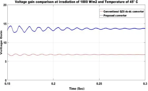
The input is varied to the combination of 1000 W/m2 and 35° C and the voltage gain with this combination is shown in Fig. 25 for both proposed converter and as well as the conventional converter. The voltage gain of the proposed converter is found to be at 13.7 and the same with the conventional converter is found to be at 6.78. The duty cycle is kept remaining at 0.43.
Fig. 23. Comparison of voltage gain offered by proposed converter and Conventional QZS dc-dc converter at Irradiation of 500 W/m2 and 45° C
Temperature
Fig. 26. Comparison of voltage gain offered by proposed converter and Conventional QZS dc-dc converter at Irradiation of 1000 W/m2 and 25° C
Temperature
The final combination is made with irradiation of 1000 W/m2 and temperature of 45° C and supplied to the PV module connected to the input of the converter under observation. The result obtained through simulation are shown in Fig. 26. The duty cycle is still kept constant at 0.43. The proposed converter provided a voltage gain of 13.8 under above mentioned conditions while the conventional converter could achieve a voltage gain of 6.78.
Fig. 25. Comparison of voltage gain offered by proposed converter and Conventional QZS dc-dc converter at Irradiation of 1000 W/m2 and 35° C
Temperature
Fig. 26. Comparison of voltage gain offered by proposed converter and Conventional QZS dc-dc converter at Irradiation of 1000 W/m2 and 45° C
Temperature
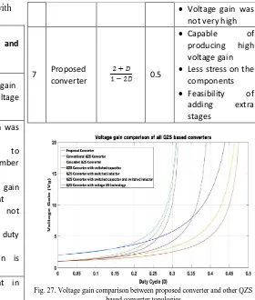
D. Comparison of proposed converter with other QZS based dc-dc converter topologies
As shown in Table IV the proposed converter can achieve higher voltage gain than the other topologies of QZS based converters. It displays capability of high step up with less number of switches and without any limitation of the duty cycle as compared to the other topologies of QZS converters. It has also been displayed that the duty cycle of the switch can be varied to the maximum value of 50%.
In order to provide a comparison of voltage gain among various QZS based converter topologies a comparative graph is prepared. The graph is displayed in Fig. 27 where variation of voltage gain against the duty cycle is shown for different converter topologies. From a close investigation it can be noticed that the curves has steeper slop for the QZS converters other than the proposed converters while duty cycle is near Dmax.
In order to provide a comparison of voltage gain among various QZS based converter topologies a comparative graph is prepared. The graph is displayed in Fig. 27 where variation of voltage gain against the duty cycle is shown for different converter topologies. From a close investigation it can be noticed that the curves has steeper slop for the QZS converters other than the proposed converters while duty cycle is near Dmax.
The above mentioned observation lead us to a conclusion that the while explained theoretically, it is possible for other converters also to achieve a high voltage gain. But the same is less probable is achieve in actual practice. On the other hand the voltage gain versus duty cycle curve shows a mild slope and can be stated to be capable of delivering high voltage gain even if it is operated at duty cycle near to Dmax.
[image:8.595.312.553.54.202.2]International Journal of Innovative Technology and Exploring Engineering (IJITEE) ISSN: 2278-3075,Volume-8, Issue-9S4, July 2019 Table IV: Comparison of the proposed converter with
other QZS based technology
S. N.
Name of Topology Voltage Gain Max . duty cycle
Advantages and
shortcomings
1
Basic QZS based dc-dc converter
0.5
Low voltage gain
High voltage
stress
2
Cascaded QZS dc-dc converter [42]
0.33
Voltage gain was increased
Possibility to
extend number of stages
Voltage gain
improvement
was not
significant
Limited duty
cycle
Voltage gain is
still low
3
QZS dc-dc converter with switched capacitor [43] 0.5
Improvement in
voltage gain
Reduction in
voltage stress
The voltage gain
is still not
satisfactory 4 Switched inductor QZS converter [44] 0.41
Voltage gain was further improved
Limited duty
cycle
Increased voltage
stress
Voltage gain was not very high
5 Active switched capacitor and switched inductor QZS converter [45] 0.33
Voltage gain was further improved
Limited duty
cycle
Increased voltage
stress
Increased
number of
switches
Voltage gain was not very high
6 QZS converter with voltage lift technique s
0.33
Improvement in
voltage gain was further improved
Limited duty
cycle
Increased voltage
stress
Voltage gain was not very high
7 Proposed
converter 0.5
Capable of
producing high
voltage gain
Less stress on the components
Feasibility of
adding extra
stages
Fig. 27. Voltage gain comparison between proposed converter and other QZS based converter topologies
Therefore, it can be conclude that the in case of the QZS converters other than the proposed converter although the voltage gain is improved but at the same time voltage stress on the diodes and switches is also significantly increased. The aforementioned effect may cause and adverse effect on reliability of the components and consequently reduces reliability of overall system.
Furthermore, the increased voltage stress also lead to the requirement of high voltage and rating switches. While the converters are used for high voltage applications the power and voltage rating required for the switches and diodes is even higher than that of the load. This consequents high cost of the system. In addition to this high voltage stress also leads to high power loss and lower efficiency of the converter and restricts voltage gain of the converter in practical applications.
In contrast while the proposed converter is used to achieve high step up of voltage for high voltage gain application the voltage stress on the switches and diodes is quite less as compared to the other QZS based converter topologies. Thus it is possible to obtain very high voltage with the proposed converter in practical applications also. As per the above discussion the achievement of high voltage gain without limiting the duty cycle of the converter and without increasing voltage stress on the switching devices and diodes can be considered as main advantages of the proposed converter over the other QZS converter topologies. This also leads us to the conclusion that the proposed converter is more reliable and efficient due to
The proposed converter is also capable of multiplying its voltage gain by adding extra stages to its existing structure. The number of stages can be increased by reparation of the portion that consist of C3, C4, D2, and L3. The voltage gain
relationship for K-stage configuration of the proposed converter is given in equation (41).
(41) Equation (41) illustrates that any level of desired voltage gain can be achieved by using multiple stages of proposed converter. It should also be noted that the voltage stress on the switches and diodes as well as the availability of voltage gain up to 50% is still persists with multistage use of the proposed converter.
After discussing the benefits of the proposed converter is worthwhile mentioning that when compared other QZS based converter topologies the proposed converter includes a drawback that the input and output does not share a common ground. This concern is only considerable when it is necessary to have a common ground between input and output.
V. CONCLUSION
As per the proposed work a QZS based dc-dc converter is derived which is able to provide high voltage gain and can derive a high voltage output while connected to low voltage output of a PV module. During this chapter the advantages of proposed converter over the other converter topologies of QZS based converters are mentioned. The aim of the proposed work was to derive a boost converter for PV applications in order to achieve its suitability for high voltage applications.
The performance of the proposed converter is examined through MATLAB simulation for various conditions of the input. A comparative study is also performed in order to identify superiority of the proposed converter over other QZS based dc-dc converters. The theoretical explanations and the simulation results obtained lead us to the following conclusions.
1.The proposed converter can resolve the issue of low voltage gain of the basic QZS based converter. 2.It performs the above mentioned action without
increasing the voltage stress on switching devices and the diodes.
3.The proposed converter provided a wide range of duty cycle up to the maximum value of 0.5.
4.Low voltage stress feature of the proposed converter equips it with high reliability and efficiency. 5.It is also possible for the novel converter to multiply
its voltage gain with multiple stages of the proposed structure and it also noticed that the voltage stress on switches and diodes remains unchanged even after using multiple stages of the proposed converter.
The study also presented a comparison of proposed novel QZS based dc-dc converter and other topologies of QZS based converters. Keeping in view the results obtained through the comparison the preeminence of the proposed converter is also confirmed in terms of voltage gain, duty cycle limitation, voltage stress and consequently reliability
and efficiency. Through the simulation results it was confirmed that the proposed novel converter can offer a voltage gain even up to 15 at a duty cycle of 0.43. This means a considerable voltage gain at a significant margin from its maximum duty cycle which is 0.5.
Owing to the confirmed benefits of the proposed novel converter such continuous input current, high voltage gain and low voltage stress it can be an appropriate option for variety of applications of low voltage output generations such as Photovoltaic system and fuel cells.
REFERENCES
[1] Wuhua Li and Xiangning He, “Review of Nonisolated High-Step-Up DC/DC Converters in PhotovoltaicGrid-Connected Applications”, IEEE Transactions on Industrial Electronics, vol. 58, no. 4, April 2011. [2] Fang Zheng Peng, “Z-Source Inverter”, IEEE Transactions on Industry
Applications, vol. 39, no. 2, March/April 2003.
[3] Fan Zhang1, Xupeng Fang, Fang Z. Pengand Zhaoming Qian, “A New Three-Phase AC-AC Z-source Converter”, Twenty-First Annual IEEE Applied Power Electronics Conference and Exposition, 2006.
[4] Yu Tang, Shaojun Xieand Chaohua Zhang, “Z-Source AC–AC Converters SolvingCommutation Problem”, IEEE Transactions on Power Electronics, vol. 22, no. 6, November 2007.
[5] Minh-Khai Nguyen, Young-Gook Jung and Young-Cheol Lim, “Single-Phase Quasi-Z-Source AC-AC Converterwith Safe-Commutation Strategy”, IEEE International Power Electronics Conference, 2010.
[6] Honnyong Cha, Fang Zheng Pengand Dong-Wook Yoo, “Distributed Impedance Network (Z-Network) DC–DC Converter”, IEEE Transactions on Power Electronics, vol. 25, no. 11, November 2010. [7] Dmitri Vinnikovand Indrek Roasto, “Quasi-Z-Source-Based Isolated
DC/DC Converters for Distributed Power Generation”, IEEE Transactions on Industrial Electronics, vol. 58, no. 1, January 2011. [8] Hanyun Shen, Bo Zhang, Dongyuan Qiu and Liping Zhou, “A Common
Grounded Z-Source DC-DCConverter with High Voltage Gain”, IEEE Transactions on Industrial Electronics, vol. 63, no. 5, May 2016. [9] Hafiz Furqan Ahmed, Honnyong Cha, Su-Han Kim and Heung-Geun
Kim, “Switched-Coupled-Inductor Quasi-Z-Source Inverter”, IEEE Transactions on Power Electronics, vol. 31, no. 2, February 2016. [10] Alexandre Battiston, El-Hadj Miliani, Serge Pierfederici and Farid
Meibody-Tabar, “A Novel Quasi-Z-Source Inverter Topology WithSpecial Coupled Inductors For Input CurrentRipples Cancellation”, IEEE Transactions on Power Electronics, vol. 31, no. 3, March 2016. [11] Geoffrey R. Walkerand Paul C. Sernia, “Cascaded DC–DC Converter
Connection ofPhotovoltaic Modules”, IEEE Transactions on Power Electronics, vol. 19, no. 4, July 2004.
[12] Dmitri Vinnikov, Indrek Roasto, Ryszard Strzelecki and Marek Adamowicz, “Step-Up DC/DC Converters With CascadedQuasi-Z-Source Network”, IEEE Transactions on Industrial Electronics, vol. 59, no. 10, October 2012.
[13] Dongsen Sun, Baoming Ge, Weihua Liang, Haitham Abu-Rub and Fang Zheng Peng, “An Energy Stored Quasi-Z Source CascadeMultilevel Inverter Based Photovoltaic PowerGeneration System”, IEEE Transactions on Industrial Electronics, vol. 62, no. 9, September 2015. [14] Yushan Liu Baoming Ge and Haitham Abu-Rub, “Modelling and
controller design of quasi-Z-sourcecascaded multilevel inverter-based three-phasegrid-tie photovoltaic power system”, IET Renewable Power Generation, 2014.
[15] Mohammad Mehdi Haji-Esmaeili, Mersad Naseri, Hossein Khoun-Jahan, and Mehdi Abapour, “Fault-Tolerant and Reliable Structure for Cascaded Quasi-Z Source DC-DC Converter”, IEEE Transactions on Power Electronics, vol. 32, no. 8, August 2017.
International Journal of Innovative Technology and Exploring Engineering (IJITEE) ISSN: 2278-3075,Volume-8, Issue-9S4, July 2019 [17] Minh-Khai Nguyen, Young-Cheol Lim and Geum-Bae Cho,
“Switched-Inductor Quasi-Z-Source Inverter”, IEEE Transactions on Power Electronics, vol. 26, no. 11, November 2011.
[18] Anh-Vu Ho, Tae-Won Chun and Heung-Geun Kim, “Extended Boost Active-Switched-Capacitor /Switched-Inductor Quasi-Z-Source Inverters”, IEEE Transactions on Power Electronics, vol. 30, no. 10, October 2015.
AUTHORS PROFILE
Mr. Manish Sharma, Assistant Professor, Department of Electrical Engineering, Poornima Institute of Engineering and Technology, Jaipur since July, 2013. M. Tech. in Power Electronics and Electrical Drives. Total 4 publications in reputed international journals including one IEEE publication.