!! !"# "
# $ % # !
& ! $
! " # #$ % &
Abstract
The design of an in-vehicle textual display system based on a matrix of light emitting diodes was achieved within this project. The concept of an illuminated display was researched, designed and developed into a working prototype.
The prototype of the display consists of eleven display sections, each consisting of a 5x7 LED matrix. The design allows these modular sections to be added or removed to vary the length of the display required.
The research into existing LED displays revealed a number of equally suited products was available, however, the goal of the project was the creation of an original design that could be manufactured into a new product in the future.
The display is controlled by a PIC microcontroller that outputs serial data to a series of cascaded serial-in parallel-out shift registers. The shift registers convert the stream of serial data to a parallel sequence used to scan each line of the display.
A handheld programmer is incorporated in the design and is used to create messages for the display. The programmer is based around a mobile phone layout using an alphanumeric keypad and multi-tap typing to enter each character.
! $ !
ENG4111/2 Research Project
Limitations of Use
The Council of the University of Southern Queensland, its Faculty of Engineering and Surveying, and the staff of the University of Southern Queensland, do not accept any responsibility for the truth, accuracy or completeness of material contained within or associated with this dissertation.
Persons using all or any part of this material do so at their own risk, and not at the risk of the Council of the University of Southern Queensland, its Faculty of Engineering and Surveying or the staff of the University of Southern Queensland.
This dissertation reports an educational exercise and has no purpose or validity beyond this exercise. The sole purpose of the course pair entitled “Research Project” is to contribute to the overall education within the student’s chosen degree program. This document, the associated hardware, software, drawings, and other material set out in the associated appendices should not be used for any other purpose: if they are so used, it is entirely at the risk of the user.
Prof G Baker Dean
Certification
I certify that the ideas, designs and experimental work, results, analyses and conclusions set out in this dissertation are entirely my own effort, except where otherwise indicated and acknowledged.
I further certify that the work is original and has not been previously submitted for assessment in any other course or institution, except where specifically stated.
Michael Costa
Student Number: 0011221440
____________________________ Signature
Acknowledgments
I would like to acknowledge the ideas and assistance provided by my fellow students and friends at USQ throughout this project. For their support with technical knowledge and assistance with the dissertation I’m very grateful.
I would to thank my supervisor, Mr Mark Phythian, for his guidance and advice, as well as Ross Leamon for proposing and supporting the project.
Table of Contents
Abstract... ii
Certification... iv
List of Figures... ix
List of Tables ... xi
Glossary of Terms... xii
Chapter 1 Introduction ... 1
1.1 Project Aim... 1
1.2 Objectives ... 2
1.3 Display Systems ... 3
1.4 Development of the Functional Specifications... 4
1.5 Dissertation Overview... 6
Chapter 2 Background Research... 7
2.1. Light Emitting Diode Technology ... 7
2.1.1 Expansion of LED Usage... 9
2.1.2 Characteristics of LED Operation... 9
2.2 Display Scanning... 11
2.3 Comparison of Market Products ... 14
2.3 RS-232 Serial Communication ... 18
Chapter 3 System Design ... 21
3.1 Description of Intended Use and Operation ... 21
3.2 Component Selection and Design Considerations... 22
3.2.1 PIC Microcontroller ... 23
3.2.2 Light Emitting Diode Modules ... 29
3.2.3 Serial-In Parallel-Out Shift Registers ... 30
3.2.5 Column Selecting Transistors ... 33
3.2.6 Message Selector... 34
3.2.7 Control Circuitry Power Supply ... 35
3.2.8 Switching Power Supply for the LED Displays... 36
3.2.9 RS-232 Transceivers ... 38
3.3 Handheld Programmer Components... 39
3.3.1 Liquid Crystal Display ... 40
3.3.2 Alphanumeric Keypad ... 41
3.4 Display Schematic ... 42
3.5 Programmer Schematic ... 43
Chapter 4 Implementation... 44
4.1 Prototype Construction... 44
4.2 Low-Voltage Programmer Construction ... 49
Chapter 5 Testing and Problems ... 51
5.1 Testing Procedure... 51
Chapter 6 Software Development... 57
6.1 MikroC Development Environment ... 57
6.2 PICpgm Development Programmer... 59
6.3 Code Developed For The Display... 60
Chapter 7 Production Related Issues ... 63
7.1 Ultraviolet Protection for the Display Case... 63
7.2 Ingress Protection for Electronic Enclosures... 65
7.3 Electro-Magnetic Compatibility... 68
7.4 Modularity and Ease of Assembly... 69
7.5 Aesthetics and Consumer Demand ... 69
7.6 Legal Issues... 70
Chapter 8 Conclusion... 72
8.1 Evaluation of the Design and Prototype ... 72
8.3 Achievement of Objectives ... 74
References... 75
Appendix A... 77
Project Specification... 77
Appendix B ... 79
Circuit Schematics... 79
Appendix C... 82
Code Listing... 82
Appendix D... 90
List of Figures
Figure 2.1 Light Emitting Diode ... 8
Figure 2.2 Rapid Scanning of the LED Display... 11
Figure 2.3 Observer’s Perception Caused by Visual Persistence ... 11
Figure 2.4 Jumbo Screen LED Modules... 14
Figure 2.5 Alpha Window Display Produced by Adaptive Micro Systems... 17
Figure 2.6 GY2200 Large Alphanumeric Display ... 17
Figure 2.7 9-Pin D Connector... 18
Figure 2.8 D Connector Pin Numbering... 19
Figure 3.1 Microchip PIC16F877A pin configuration ... 23
Figure 3.2 Harvard and von-Neumann Processor Architecture ... 26
Figure 3.3 Single Cycle Instruction Operations... 28
Figure 3.4 LED Package Dimensions & Circuit Diagram... 29
Figure 3.5 Conversion from Serial to Parallel Data ... 30
Figure 3.6 Pin configuration of the 74HC595 shift register ... 31
Figure 3.7 Pin Configuration of ULN2003A Darlington Array... 32
Figure 3.8 Binary Coded Decimal Thumbwheel... 34
Figure 3.9 Pin Configuration of Voltage Regulator ... 35
Figure 3.10 Pin Configuration of Switching Voltage Regulator... 36
Figure 3.11 Switching Voltage Regulator Circuit... 37
Figure 3.12 Pin configuration of Maxim RS-232 Transceiver ... 38
Figure 3.13 Liquid Crystal Display ... 40
Figure 3.14 Multi-tap Keypad Layout ... 41
Figure 3.15 Alphanumeric Keypad ... 41
Figure 4.1 Stripboard Mounted with IC Sockets... 46
Figure 4.2 Initial Display Prototype ... 46
Figure 4.3 Programmer Prototype ... 47
Figure 4.4 Serial Link Message... 48
Figure 4.5 Programmer Prototype ... 48
Figure 4.6 Low-Voltage Programmer Schematic ... 50
Figure 5.1 Initial Displays Tested ... 53
Figure 5.2 Initial Display Test ... 55
Figure 6.1 MikroC Integrated Development Environment... 58
Figure 6.2 PICpgm Development Programmer... 59
List of Tables
Table 2.1 Common LED Compounds and Wavelengths... 8
Table 2.4 RS-232 Pin Description ... 19
Table 3.1 PIC16F877A Port Features ... 24
Table 7.1 Foreign Bodies Protection Index for IP Ratings... 65
Table 7.2 Water Protection Index for IP Ratings... 66
Glossary of Terms
ASCII – American Standard Code for Information Interchange: A character set and form of character encoding which represents text in computers and other communications equipment.
BCD – Binary Coded Decimal: A common form of encoding for decimal digits in computing and electronics equipment. Each digit is represented by four binary bits which have values from left to right of 8, 4, 2 and 1. The sum of these four bits equals the equivalent decimal value which ranges from 0-9.
CMOS - Complementary Metal Oxide Semiconductor: A widely used type of integrated circuit design which uses significantly less power that other forms of logic.
CPU – Central Processing Unit: The circuitry of a computer that executes calculations, also known as a processor. Two typical components of a CPU are the arithmetic logic unit (ALU), which performs arithmetic and logical operations, and the control unit, which extracts instructions from memory, decodes and executes them.
DIL – Dual-In-Line (package): A standard of electronic component layout where pins on the device are aligned in two parallel lines.
EMI – Electro-Magnetic Interference: Radiated or conducted energy that adversely affects circuit performance disrupting a device’s normal operation.
IC – Integrated Circuit: A set of electronic components and their interconnections that are etched or imprinted on a semiconductor substrate.
IDE – Integrated Development Environment: A set of programs run from a single user interface. Programming languages often include a text editor, compiler and debugger, which are all activated and function from a common menu.
I/O – Input and Output: Conductors used to transfer data between a central and a peripheral device.
IP – Ingress Protection: A classification of the level of protection that electrical appliances provide against the intrusion of solid objects, dust, accidental contact, and water.
LED – Light Emitting Diode: A semiconductor device that emits narrow-spectrum light when electrically biased in the forward direction.
PC - Personal Computers: A microcomputer intended to be used by one person at a time, and suitable for general purpose tasks such as word processing, programming, or game play.
PIC – Programmable Integrated Circuit: A family of microcontrollers made by Microchip Technology.
RISC – Reduced Instruction Set Computing: A microprocessor CPU design philosophy that favours a smaller and simpler set of instructions to streamline processing.
Chapter 1 Introduction
1.1 Project Aim
The aim of this research project is the development of an in-vehicle textual display system based on a light emitting diode (LED) dot matrix. The project involves taking the device from an initial concept through a design phase, to constructing a prototype of the product. The system consists of the central display unit accompanied by a handheld interface to program messages into the display. The request for the design originated from Downey Engineering, a Toowoomba based electronics and control business that has sponsored the project. They are interested in creating the design as they have identified an opportunity in the market for such a product and may produce the device in the future.
1.2 Objectives
The main objectives accomplished in this project include:
1. Research information relating to the design of LED moving message displays and microcontroller based circuits.
2. Design a microcontroller driven, marquee type display to be mounted in a vehicle.
3. Design a handheld interface to the display system for calling up and programming messages.
4. Design software to provide pre-programmed messages, animations and user defined messages for the display system.
5. Develop a full set of working specifications of the display system to suit the technical / budget limitations of the project.
6. Construct a prototype of the display system mentioned in 2 and 3 above and evaluate its performance.
1.3 Display Systems
The project is derived from a proposal made by Downey Engineering to fund the design of an illuminated display; an initial step was the evaluation of the requirements that needed to be met. This was achieved through several consultations with Ross Leamon, the manager of engineering at Downey Engineering. In these meetings the technical features, physical operation and possible applications for the design were addressed. These discussions resulted in a functional specification that outlined the purpose and features that the design would ultimately fulfil. This document could then be used as a benchmark, against which created designs could be assessed for their merit.
1.4 Development of the Functional Specifications
The starting point for the design aspect of the project was a flexible functional specification drafted by Downey Engineering. This document defined the need for an in-vehicle/industrial style of display that is both robust and economical. The technical features, physical operation and possible applications for the display were also discussed, however any limits placed on the design were negotiable. The only distinct specifications were:
• Voltage Supply Range: 10-30 volts DC • Operating Temperature: 0-50 degrees Celsius • Display Visibility: 20-30 metres
• Message Capacity: 90 messages
• Text Effects: Static, Scrolling, Flashing • Accompanying handheld message programmer
A voltage supply range of 10-30 volts was chosen so the display was a versatile product that could operate in a number of applications. The 12V supply system of automotive vehicles is the primary intended voltage for the display, but systems that use 24 volts are not uncommon and were therefore incorporated into the specification. The operating temperature of 0-50 degrees Celsius was included as a requirement as these temperatures are considered to be the extreme temperatures that may be reached inside an average vehicle. As most integrated circuits and electronic parts that could be used in the design are rated for temperatures ranging well outside these limits, this requirement poses no great limit on the design.
1.5 Dissertation Overview
CHAPTER 2 introduces the background research and information relating to the design of the display, existing systems available and the design and performance requirements of the project.
In CHAPTER 3 the intended use and operation of the whole display is described. A description of the components used in the design and an explanation of how they are interfaced, is followed by a schematic of the display and handheld programmer.
CHAPTER 4 addresses the development of the prototypes of display and programmer focusing on the methods of construction.
CHAPTER 5 will detail the processes used for testing the display and handheld interface prototypes, while in construction and after completion.
CHAPTER 6 presents the software used in developing code for the display system as well as an explanation of additional the routines developed.
CHAPTER 7 discusses some of the broader issues that relate to the creation of the product including legal issues, aesthetics and electromagnetic compatibility.
Chapter 2 Background Research
2.1. Light Emitting Diode Technology
Illuminated textual displays based on light emitting diodes (LEDs) are quite a widely used medium, used to convey information in modern society. The use of light to display text and information is a well established technology, as it is both eye-catching during the day and easily visible at night. Neon lighting and incandescent bulbs have been utilized in this application for large advertising displays since the early 1920’s. With the creation of semiconductor technology came the increased usage of LEDs in illuminated displays due to their high efficiency and long lifespan.
LEDs consist of a semiconductor material that has had impurity atoms introduced into it through a process called doping. The addition of different impurities changes the balance of electrons in the material, creating a N-type material that has extra free electrons or P-type material that has “holes” where electrons are scarce. Diodes consist of a section of N-type material bonded to a section of P-type material. When forward biased electrons move from the N-type region to the P-type region and holes move in the reverse direction. Electrons combine with holes of the P-type layer to release energy in the form of light. This process occurs in all diodes, but LEDs have been specifically designed to emit light in the visual or infrared range. The wavelength of the light emitted λ is given by:
g h c
E
≅ (1.1)
where h is Planck’s constant (6.626 × 10⁻³⁴ J-s);
c is the velocity of light in vacuum; and
Eg is the bandgap energy for a particular semiconductor.
photons outward from the semiconductor as shown in the following figure. The lens and the bottom reflecting surface increase the amount of light transmitted out of the top of the device.
Figure 2.1 Light Emitting Diode
Source: How Stuff Works (2005)
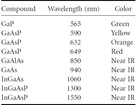
LEDs of various wavelengths are commonly available and are obtained by combining ratios of semiconductor material that have different bandgap energies. By choosing different binary, ternary, and quaternary compositions of these semiconductors a light emitting diode of particular wavelength can be created as shown in the following table.
[image:22.595.203.424.579.749.2]
2.1.1 Expansion of LED Usage
The use of a LEDs dot matrix for creating a text display system is quite common with its usage expanding greatly in recent years. Such displays can be found in airports, where they are used to display flight information, and in stock exchanges to display share prices. The wide usage of LED displays is a result of its ability to convey information to large audiences quickly and efficiently. As LED displays are often controlled by digital technology the information can swiftly and easily be updated. This feature of LED displays has led to a great flexibility of such products in countless applications. An additional benefit of using this form of display is that LEDs are a very efficient form of illumination. Unlike incandescent bulbs, LEDs do not generate a large amount of wasted energy in the form of heat.
2.1.2 Characteristics of LED Operation
The type of LEDs used for the project are the GaAsP high-efficiency red variety manufactured by Kingbright. High-efficiency red, GaAsP on a GaP substrate was the first non-low-current high-efficiency red LED. The term GaAsP represents the working chemistry of the LED, which is gallium arsenide phosphide, with an arsenic to phosphorus ratio around 40 to 60 on a gallium phosphide (GaP) substrate. The peak wavelength of the high-efficiency red GaAsP LED is usually around 630 nm. Typical drive current is 5 to 20 mA and maximum current is usually 30 mA. The typical voltage drop across the device at 20 mA is around 1.9 volts. (Klipstein 2004)
2.2 Display Scanning
[image:25.595.270.358.602.725.2]A method commonly used to control illuminated displays is to turn the rows or columns of the display on and off in quick succession. Multiplexing, as it is termed, reduces the amount of input and output (I/O) lines required to control the individual elements of a large display. In multiplexing a common set of control lines is used to join each display to the control system. As a consequence the amount of conductors and ports required for controlling is significantly reduced when compared with connecting each display individually to the system. A sub-unit of the display, typically a row or column of LEDs, is connected to the common bus, which is controlled to output the required pattern for that unit at each instant. The sub-units are then sequentially illuminated with the corresponding pattern. Repeatedly cycling through this process, called scanning is used to create the phenomena of visual persistence. An example of this process is shown in the following figures, where rapidly illuminating sections of the display causes an observer to see a single image.
Figure 2.2 Rapid Scanning of the LED Display
The theory of visual persistence is that the perceptual process of the brain and retina in the eye retain an image for a split second after viewing. David Cyganski further explains the physical process of visual persistence:
‘Although an image on the retina decays gradually, rather than lasting a specific amount of time, there is a critical period during which the stimulus changes so little that the visual system cannot take in any new information even if the eyes are open. This period, on average, is about 50 milliseconds, or one-twentieth of a second. Thus, the average human visual system can only take in about 20 different images per second before they begin to blur together. If these images are sufficiently similar, then the blurring which takes place appears to the eye to resemble motion, in the same way we discern it when an object moves smoothly in the real
world.’(Cyganski, 1998).
2.3 Comparison of Market Products
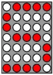
[image:28.595.200.431.440.664.2]There are numerous companies that produce textual displays similar to the design for this project. A few examples of different classes of display will be given to demonstrate the variety of products available. The simplest way to categorise LED displays is whether the information shown is purely alphanumeric, that is, consists of only characters and digits, or if the display is capable of presenting animation. Displays that are able to present animation are usually developed for large scale applications such as music concerts, sporting events or mass advertising. The common name for large scale displays of this type is “Jumbo Screens”. In a colour Jumbo Screen each pixel, the basic unit of the image, consists of a module containing at least one red, green and blue LED as shown below. These pixel modules are arranged in a rectangular grid to form the screen. The number and size of LEDs used to form one module varies with the dimensions of the full display as shown is Table 2.2.
Figure 2.4 Jumbo Screen LED Modules
Table 2.2 Jumbo Screen Dimensions
LED module size Screen size (metres)
4 mm 2.56 x 1.92
25 mm 16 x 12
40 mm 25.6 x 19.2
In a Jumbo Screen a complicated computer system is required to control which of the LEDs are to be turn on, in addition to their levels of brightness. The computer samples the input signal, usually a television signal, for the intensity and colour information of the image. This is then translated into an intensity level for the three different LED colours that exist in each of the pixel modules. When these three colours of light combine, a matching representation of the pixel in the original input signal is produced. A typical 20-metre Jumbo Screen can consume up to 1.2 Watts per pixel, which is approximately 300,000 Watts for the full screen.
The use of a Jumbo Screen and other full animation displays would be an excessive design for this project as the screen sizes are much too large for the intended application and the features of such versatile displays would not be utilized enough to warrant such a complicated design. Consequently the focus is primarily on single line alphanumeric LED displays.
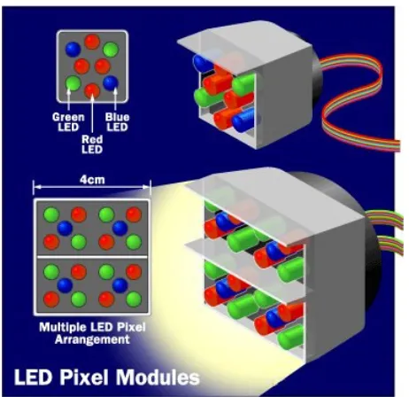
The creation of the LED display for this project clearly is not pioneering a new technology or product line, as many examples of similar devices can be found in the market today. Two comparable units that are similar to the aim for this project are the GY2200 ‘Large Alphanumeric Display’ produced by Vorne Visual Display & Productivity Tools and the ‘Alpha Window Display’ produced by Adaptive Micro Systems.
[image:30.595.115.514.436.694.2]The Alpha display is the most comparable product available to the design created for this project. It offers a large 4-inch display typically of 13 characters. In addition to the standard features of a moving message display the Alpha contains a number of additional features that may be considered in future versions of the display. These features include, a clock to display the date and time in 12 and 24-hour format, an infrared link between the display and programmer and a variable character set to provide various fonts. An image of the Alpha display in use and a full list of its features are shown below.
Table 2.3 Alpha Window Display Specifications
Figure 2.5 Alpha Window Display Produced by Adaptive Micro Systems
Source: Adaptive Micro Systems (2005)
The GY2200 alphanumeric display by Vorne, shown below, is also a comparative design although the display is to some extent smaller. Its features include:
• High-efficiency red LED display • 2" font size with a full matrix display • Smooth scrolling up to 60 characters • Interface to almost any serial device • Simple ASCII based protocol
• Five baud rates from 300 to 9600 • Viewing distances of 75' and beyond • Full 128 ASCII character set
• Quick and easy DIP switch setup •ASCII commands to scroll, flash
Figure 2.6 GY2200 Large Alphanumeric Display
Source: Vorne Visual Display & Productivity Tools (2005)
2.3 RS-232 Serial Communication
[image:32.595.222.410.422.504.2]The RS-232 serial communication standard is used for data transfer between the handheld programmer and the display unit for this project. The RS-232 standard, stands for Recommended Standard number 232 of which the latest amendment is revision D. This format of communication was selected as it is widely supported by Personal Computers (PCs), is very simplistic in construction, and is compatible with the microcontroller used in both the display and programmer. Devices that use serial communications can be divided into two categories, Data Communications Equipment (DCE) and Data Terminal Equipment (DTE). The DTE is typically a PC and the DCE is the remote device which is communicated to over the serial connection. The full RS-232 standard specifies that a 25-pin “D” connector be used, however typical PC communications use a subset of the standard with a 9-pin “D” connector as shown below.
Figure 2.7 9-Pin D Connector
Source: Arcelect (2005)
carrier-detect lines on both devices. When the data-terminal-ready line is made active, then the data-set-ready and the carrier detect immediately become active as they form the end of the loop back. A loop back is also made from request-to-send to clear-to-send on both devices. The entire configuration effectively bypass the handshaking protocols of the RS-232 standard to form a simplified communication link. The following figure shows the pin labelling of a 9-pin D connector and their usage in the RS-232 standard.
Figure 2.8 D Connector Pin Numbering
Source: Arcelect (2005)
Table 2.4 RS-232 Pin Description
D-Type-25 Pin No.
D-Type-9
Pin No. Abbreviation Full Name
Pin 2 Pin 3 TD Transmit Data
Pin 3 Pin 2 RD Receive Data
Pin 4 Pin 7 RTS Request To Send
Pin 5 Pin 8 CTS Clear To Send
Pin 6 Pin 6 DSR Data Set Ready
Pin 7 Pin 5 SG Signal Ground
Pin 8 Pin 1 CD Carrier Detect
Pin 20 Pin 4 DTR Data Terminal
The electrical parameters of the logic level in the RS-232 standard state that: • A logic 0 will be between +3 and +25 volts
• A logic 1 will be between –3 and –25 volts • The region between +3 and –3 volts is undefined.
Chapter 3 System Design
3.1 Description of Intended Use and Operation
The intended use of the display system developed in this project was initially specified for vehicle mounting, however the uses for the design remain universal. The adaptable characteristic of this type of unit means that it could be used in numerous other applications. The self-contained nature of the intended design will allow the display to be mounted almost anywhere it is required and could provide information to viewers at any of the following locations.
• Airports – Assisting passengers and pilots with flight information • Banks – To increase sales and improve service.
• Factory Automation – To increase and enhance productivity.
• Drive-Through Restaurants – To advertise new products and improve service. • Theatres – To advertise specials and guide movie patrons.
• Transportation – Assisting passengers in the event of a break down or accident.
3.2 Component Selection and Design Considerations
The primary task in developing an illuminated text display is the creation of the central control system that manages when each of the LEDs are to be on. This system needs to control a considerable amount of information in a short period of time. An illuminated display usually consists of smaller modules arranged together to from a larger screen, each module usually consisting of a 5 x 7 matrix of LEDs. The minimum number of bits that a control system has to address for a small 8 module display is 280, one bit for each LED. The goal of this project is to create a display containing approximately 12 to 16 modules. This means the control system is required to handle between 420 to 560 LEDs at any one time. As discussed previously, in section 2.2, the method of multiplexing modules reduces this figure, though the control of the entire display is still a significant feat.
Selection criteria for the control circuitry was developed out of the problem of controlling the large number of LEDs in a display. The control circuitry required: • A large number of input/output ports
• Fast operating speed
• Affordability of development tools • Easy programming
• High availability of parts for future manufacturing • Large memory capacity
• Low power consumption
Based on these criteria a Programmable Integrated Circuit (PIC) microcontroller appeared to be the best option for the task. The microcontroller selected was a PIC16F877A 40 pin Enhanced Flash Microcontroller produced by Microchip.
3.2.1 PIC Microcontroller
A PIC microcontroller is a single integrated circuit chip that contains a processor, memory storage and input and output ports (I/O), all controlled by software stored within the chip. A microcontroller has the similar function of a Central Processing Unit (CPU) found in home PCs, in that information in the form of instructions are used to control the device. A microcontroller, however, is a trimmed down industrial version that is tailored to a specific application. Generally PIC microcontrollers have less throughput of data and a smaller memory capacity when compared the CPUs of a home PC. PIC microcontrollers are grouped by the size of their instruction word. The three current PIC microcontroller families are:
1. Base-Line: 12-bit Instruction Word length 2. Mid-Range: 14-bit Instruction Word length 3. High-End: 16-bit Instruction Word length
[image:37.595.139.480.409.693.2]The following image is of the PIC16F877A microcontroller used in this project.
Figure 3.1 Microchip PIC16F877A pin configuration
The PIC16F877A is a Mid-Range 14-bit microcontroller that comes in a 40 pin dual-inline (DIL) package with 8K of flash memory and 256 bytes of EEPROM data memory. It is an extremely affordable device for the numerous features that it contains. The dual-inline-package format in which the IC is produced is easy to orientate on breadboard and stripboard projects, making connections to the pins straightforward. The flash memory it uses is a type of memory storage that has the ability to be electrically programmed and erased without the removal of the IC from the circuit. This in-circuit programming feature is a very significant advantage of the PIC16F877A, which aided in the creation of routines for the prototype. The ability to load, test and reprogram the chip while still within the circuit is an invaluable time saving feature. When selecting a microcontroller for the project it was important to choose a device with sufficient onboard memory, as the length of the final software code was unknown. The 8K of 14-bit word instructions was suitable for the estimated length of code that would be generated.
As controlling a large number of LEDs is an integral problem of the project, it necessitated that the microcontroller have the capability of handling a large number of input and output lines. The PIC16F877A has at maximum, 32 I/O lines for interfacing with other components. This number of control lines is sufficient for the intended task, but the increased number allowed more flexibility in the design phase. The I/O lines are grouped into five ports labelled A, B, C, D and E. Some additional features of these ports are shown below in Table 3.1.
Table 3.1 PIC16F877A Port Features
Name No. of
Bits Pin Name Functions
Port A 6 RA0-RA5 Digital input/output or Analogue inputs
The refresh rate of the display dictates that the control system have a fast processing speed so as to be able to process and deliver data at a rapid rate. The maximum operating frequency of the PIC16F877A is 20 MHz, which is sufficiently fast to process data for the display within the flicker fusion threshold time.
A simple programming feature was an important factor in selecting the PIC. The in-circuit programmable flash memory of the PIC16F877A is greatly beneficial as the limited budget for the project excluded the purchasing of expensive development tools. PIC microcontrollers produced by Microchip are fully supported by a range of development hardware including development boards and IC programmers. In addition to this, Microchip produces an Integrated Development Environment that contains assemblers, compilers, simulators, emulators and debugging software. The cost restraints on the project limited the purchasing of these support devices however. As a result freely available compilers and programming software was sourced from the internet and an inexpensive programmer was made on stripboard.
The supply availability of the PIC16F877A was an important deciding factor for choosing it from other Microchip PICs. This specific IC was commonly available from several electronics distributors, which is a necessity for the future manufacturing of the display.
As with most PICs the PIC16F877A contains a Reduced Instruction Set Computer (RISC) microprocessor. This type of construction increases the performance of the PIC due to the following features associated with RISC microprocessors:
Harvard Architecture
The two most common forms of processor design are the von-Neumann and Harvard architectures. The Harvard design is characterised by having the program memory and data memory as separate memories that are accessed from separate buses. This arrangement has improved bandwidth over the von-Neumann model in which the program and data memory are retrieved from the same memory using the same bus. An illustration of both forms of processor architecture are shown below.
Figure 3.2 Harvard and von-Neumann Processor Architecture
Source: Microchip (2005)
Long Word Instructions
As the Harvard architecture contains separate instruction and data buses, the instruction bit length can be made wider than the typical 8-bit data word. The large 14-bit instruction word increases the efficiency in the usage of the program memory, as the width of the program memory is optimised to suit architectural requirements of the instruction bus.
Single Word Instruction
As a result of the Harvard design, instruction opcodes are 14-bits wide, making it possible to have all single word instructions. A 14-bit wide program memory access retrieves one 14-bit instruction in a single cycle. With single word instructions, the number of program memory addresses is equal to the total number of instructions for the device. This implies that all locations are legitimate instructions. Alternatively the von Neumann architecture typically results in multi-byte instructions. A device with 4-kilobytes of program memory may therefore only contain 2K of instructions. Whilst this is a generalisation, it shows that there is no assurance that each location is a valid instruction.
Instruction Pipeline and Single Cycle Instructions
Figure 3.3 Single Cycle Instruction Operations
Source: Adapted from Microchip (2005)
3.2.2 Light Emitting Diode Modules
[image:43.595.153.479.402.679.2]In selecting the LEDs to use for the display the most freely available units were chosen for their ease of supply. These units needed to be successively side stackable to create a large rectangular matrix that forms the display screen. The most common form of modules of this type are the 5 x 7 dot matrix units which are widely available in a variety of sizes. For the first prototype a set of eleven 18mm Super Bright Red modules, produced by Kingbright, were purchased from RS Components. These displays were also preferred as they have pins that are aligned in a similar fashion to a DIL integrated circuit. The pin configuration made it easy to push in and orientate the LED modules on breadboard and stripboard, as well as making connections to the pins straightforward. The dot matrix of LEDs has a common anode connection for each of the 5 columns and a common cathode for each of the 7 rows. This feature of the LED modules is utilized for the multiplexing process. The following figure is a plan view of a single dot matrix module and its schematic.
Figure 3.4 LED Package Dimensions & Circuit Diagram
For the final display design larger versions of the Kingbright 5 x 7 dot matrix units are to be used to allow enhanced visibility of the display. These displays are approximately 40mm high and have a different pin layout to the smaller units. Using modules such as these allows for enhanced scalability in the final design. Each of the LED displays and associated circuitry becomes a discrete modular unit that can be added or removed depending on the display length required. By modularising the display units, production costs are also reduced when manufacturing the display.
3.2.3 Serial-In Parallel-Out Shift Registers
In order to obtain control over the 420 LEDs in an 11-module display, multiplexing of the I/O to the microprocessor is required. To do this, a series of serial-in to parallel-out shift registers are used to convert a stream of serial bits from the PIC to a parallel output port to the LEDs. This process effectively extends the I/O of the microcontroller by converting a serial port to a parallel one. To accomplish the large parallel output port required to address each LED, the shift registers are “daisy-chained” together. This means the serial output of one stage of the shift register sequence is cascaded to form the input to the next shift register as shown below.
Figure 3.5 Conversion from Serial to Parallel Data
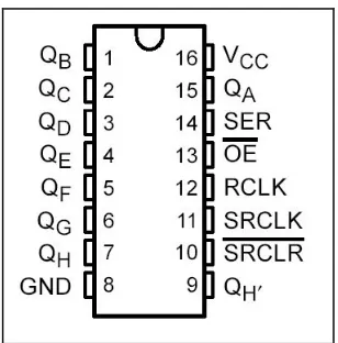
separate registers within it, a shift register and a storage register; each register is provided with a separate clocking input. In operation, individual data bits are applied to the serial data input (SER) and clocked into the shift registers using the shift register clock pin (SRCLK). Once the entire 8 bits of serial data have been entered, the data can then be latched into the storage register where it becomes the parallel output. The output is latched by a positive-edge trigger on the storage register clock pin (RCLK).
Figure 3.6 Pin configuration of the 74HC595 shift register
Source: Texas Instruments (2005)
When connected in this cascading manner, the shift register overflow pin (QH`) is
3.2.4 Current Drivers
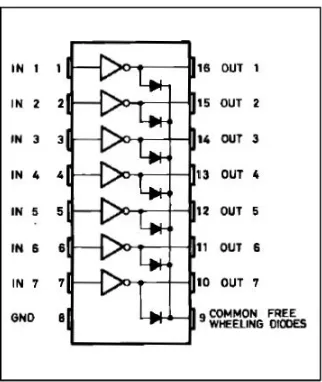
[image:46.595.234.395.460.651.2]The parallel outputs of the shift registers are not rated to handle enough current to illuminate the LEDs that they control. To get full illumination of the LEDs in the prototype, each will be pulsed with 50mA, which is above the 35mA rating of the 74HC595. As a result, current drivers are used to supply each LED with enough current to fully illuminate. The devices used are ULN2003A that contain seven high current darlington arrays. All darlington pairs have an open collector which forms the input channels of the IC, and all pairs have a common emitter which is grounded. Each channel is capable of withstanding 500mA and the inputs are pinned opposite the outputs to simplify the layout on a board. The large parallel output created from the shift registers is the input to each of these arrays, which control the pattern of LEDs that are turned on. As the darlington arrays are configured as an open collector and a grounded emitter, they in fact control the LEDs by sinking current, effectively becoming an inverter which is represented in the image below. The current drivers are subsequently used to control the pattern of LEDs in a single column that are provided with a path to ground. Each column is then routinely illuminated by power supplied through a column selecting transistor for the multiplexing process.
Figure 3.7 Pin Configuration of ULN2003A Darlington Array
3.2.5 Column Selecting Transistors
3.2.6 Message Selector
The operation of the display is designed so that a series of short messages can be stored in the display using the programmer, and that each message can be called up using the message selector. A Binary Coded Decimal (BCD) pushbutton thumbwheel is used to select the required message for the display. The device, shown in the image below, contains up and down press buttons that are used to rotate the number wheel. The wheel displays the current number from 0 through to 9. The output pins of the device are designed to encode the current value on the wheel into the binary coded decimal format. The thumbwheels are made to snap together side by side to increase the values that can be selected. Two BCD thumbwheels are used in the design, which in combination can be used to select from messages 00 through to 99.
Figure 3.8 Binary Coded Decimal Thumbwheel
3.2.7 Control Circuitry Power Supply
[image:49.595.222.406.296.446.2]As the display is designed for use in a vehicle/industrial application it will be powered from a 12-30V DC supply. The display and programmer both use CMOS logic technology which typically operates at a voltage level of between 2V and 5.5V. To meet these needs a LM7805 series voltage regulator, shown in the image below, is used to step down the voltage to a fixed level of 5 volts. This is an optimum level for CMOS logic systems and is achieved with minimal external components to the regulator. Filter capacitors are also incorporated into the power supply circuit to filter out unwanted noise generated by the electronic systems of the cars engine.
Figure 3.9 Pin Configuration of Voltage Regulator
3.2.8 Switching Power Supply for the LED Displays
In providing power to the display it was realised that the LED matrix would consume a significant amount of power when compared to the control circuitry. It was estimated that the display at peak operation would draw 4A of current running at 5V. It was evident that a simple linear voltage regulator would not be sufficient for the power supply circuit. A linear regulator that reduces the voltage from 12V to 5V with an output of 4A would generate a significant amount of waste heat in the process. This design would be very inefficient; furthermore a linear voltage regulator capable of outputting 4A would require a bulky heat sink for dissipating waste heat. It was decided that two voltage regulated circuits be incorporated in the display; one linear voltage regulator to supply the low current to the control circuitry such as the PIC microcontroller and shift registers and another switching step-down voltage regulator for the higher current drawn by the display. The regulator used in the design is a National Semiconductor LM2576, which is shown in the image below. This integrated circuit is ideal for the application, as it requires a minimum number of external components. The adjustable version of this IC is used so that the voltage to the display LEDs can be varied to allow brightness control to be included in the design.
Figure 3.10 Pin Configuration of Switching Voltage Regulator
Source: National Semiconductor (2005)
modules. The values of resistors R1 and R2 will need to be selected in further prototypes to suit the range of voltages required for the larger LEDs used.
Figure 3.11 Switching Voltage Regulator Circuit
3.2.9 RS-232 Transceivers
[image:52.595.218.410.380.596.2]For the communication between the handheld programmer and the display unit, the RS-232 communication standard was used due to its ease of implementation and its wide usage in areas of communication. The serial communication was also chosen as the PIC microcontroller contains a Universal Synchronous Asynchronous Receiver Transmitter (USART), which is fully integrated in hardware. The USART transmits and receives data at the 5V levels of CMOS logic, while the standard for RS-232 communication requires logic levels of approximately ±10V. To overcome the difference in logic levels a Maxim MAX202 RS-232 transceiver IC, shown below, is used as an interface. This IC produces the required ±10V for RS-232 communication when supplied from a 5V source. When data is transmitted to the display using the serial connection, the MAX202 converts the signal to the CMOS levels used by the microcontroller.
Figure 3.12 Pin configuration of Maxim RS-232 Transceiver
3.3 Handheld Programmer Components
The creation of the handheld programmer was done with special attention to a user-friendly approach for the design. The handheld programmer is based primarily with a mobile phone layout in mind. The familiarity with mobile phones in today’s society has prompted this decision. An arrangement similar to creating and sending text messages on a mobile phone was used. The primary control circuity that is used in the programmer is the PIC16F877A microcontroller that is also used in the display. The choice to use the same microcontroller for both devices was clearly beneficial. By duplicating the control circuitry from the display to the programmer, time was saved in the prototyping and testing phase due to the ease of reproduction once an initial circuit is made. The additional devices the microcontroller interfaces with in the programmer includes a liquid crystal display (LCD), a 4x4 alphanumeric keypad and a Maxim RS-232 transceiver chip.
3.3.1 Liquid Crystal Display
A QP5515 two line 16 character LCD display is used in the project to display the massages created on the programmer unit before they are loaded into the display. The LCD can be interfaced with the microcontroller in either a 4-bit or 8-bit data bus mode. The 4-bit mode was chosen for the design so as to conserve the number of I/O lines used in the microcontroller. There are six other control lines used to operate the device. Positive and negative supply lines are used to power the device and an adjustable contrast line that varies the screen intensity as the input voltage is varied from 0 to +5 volts. Additionally, the enable signal, read/write and register select lines are other lines used for addressing and selecting the LCD. The LCD also contains a complete onboard ASCII set and can therefore display any of the characters that may be used on the LED display system.
[image:54.595.194.438.362.471.2]3.3.2 Alphanumeric Keypad
[image:55.595.231.401.380.528.2]An alphanumeric keypad was used in the programmer to more closely resemble the mobile phone layout. The familiarity of most people with creating text messages with such keypads prompted this decision. Another significant advantage of the alphanumeric keypad when compared to the typical QWERTY style keyboard, used for computers, is the considerable reduction is size. By using a small keypad of this size the programmer remains very compact while still providing the full amount of characters available from the normal QWERTY keyboard. To provide the type of user input typical of mobile phones, an input method termed multi-tap is used. In this method the user repeatedly presses a button of the keypad to scroll through the letters allocated to that button. For example, pressing the button labelled ‘5’ once would present the letter ‘J’, if press a second time the letter ‘K’, a third time the letter ‘L’ and finally the numeral ‘5’. An image of the keypad used is shown below along with letters associated with each button in multi-tap.
Figure 3.14 Multi-tap Keypad Layout
[image:55.595.236.394.567.720.2]Chapter 4 Implementation
4.1 Prototype Construction
In developing the first prototype for the project, time and expense were the most important factors under consideration. The prototype was constructed in order to test the physical viability of the design, ensuring that the circuitry operated as expected. The initial construction needed to be completed promptly to meet the deadlines of the project and to allow time for correcting any faults. The prototype was developed extremely economically using several breadboards and stripboard on which the components were mounted. Through this type of construction, modifications could be easily made before entering into the development of larger scale, and more costly prototypes.
The master clear pin MCLR is an active low reset to the PIC16F877A and was therefore connected to Vcc using a pull-up resistor. This prevents the microcontroller from resetting during operation. In the final design a pushbutton may be incorporated to pull the MCLR pin low as a master reset to the display. The microcontroller was programmed in low voltage mode, such that a voltage source of only +5V was needed to download code in the PIC’s memory. In the low-voltage programming mode a 1k resistor is required on pin RB3 to ground to ensure continued operation. In this mode RB3 is dedicated to the programming function and ceases to be used as a general purpose I/O pin. Although the loss of one of the pins on the 8-bit port was troublesome it was an acceptable loss for saving money on buying a specialised PIC programmer.
Figure 4.1 Stripboard Mounted with IC Sockets
Using stripboard and IC sockets, although very inexpensive, it was also extremely time consuming. Each connection on the board needed to be individually soldered, including all the wiring connections. The copper strips on the reverse side of the board also required cutting in specific places to isolate components, which again was extremely time consuming. An image of the finished prototype display is shown below.
Figure 4.2 Initial Display Prototype
[image:60.595.116.517.420.601.2]alone. Due to this, the linear regulator was only used to power one display at a time for testing purposes while the switching regulator was being built.
After constructing the display of the first prototype, the circuitry for the serial connection between the handheld programmer and the display unit was developed. This circuit consists of a Maxim RS-232 transceiver IC and additional external capacitors. The purpose of this circuit is to modify the voltage levels of the inputs from the CMOS logic of the microcontroller to the RS-232 serial communication voltage levels typically ±10 volts. Once the serial link was built, communication to a PC was tested by running a communication terminal program, which confirmed the serial data transfer. As the handheld programmer was not yet complete, the PC was an effective substitute as it also can be used to program the display. The serial link to the display was verified using a routine that received a character typed in the terminal program on a PC. The routine immediately returned the same character that was received via the serial link. The routine effectively received data from the PC and bounced it straight back. This established that the circuit and software created worked correctly and could be used if implemented in both units to send data between the handheld programmer and the display.
[image:61.595.124.507.530.732.2]A prototype of the handheld programmer was then constructed to test the circuit’s feasibility. An image of the prototype developed on a breadboard is shown below.
This circuit was subsequently used to create messages using the keypad; each was displayed via the LCD. The serial transceiver was then implemented with the programmer allowing the prototype to transmit the created messages via the serial link to a PC. The addition of the serial link and the message transmitted is shown in the images below.
Figure 4.4 Serial Link Message
[image:62.595.137.495.429.709.2]4.2 Low-Voltage Programmer Construction
Figure 4.6 Low-Voltage Programmer Schematic
Source: Christian Stadler (2004)
[image:64.595.127.505.491.716.2]Chapter 5 Testing and Problems
5.1 Testing Procedure
The procedure of continually testing the circuity as it was progressively built upon, was an essential part in maintaining the integrity of the design. As each new section of the system was developed, it was tested to see that it functioned properly, and then integrated with the existing circuitry. Finally the combined circuit was tested to verify that jointly both systems operated as expected. This process of testing in a modular fashion ensured that once a new module was constructed it was checked for faults before integrating it with the existing system.
The first form of testing done was on the low-voltage PIC programmer and microcontroller circuit. It was important to establish the functionality of this circuit, as it forms the central control for all other parts of the system. The microcontroller and low-voltage programmer were constructed and a series of simple experimental programs were developed to test each of them. These programs were designed to ensure that the programmer performed its task adequately and also to help better understand the control of the ports on the PIC16F877A. As this was the first time for using this particular device and associated software, it was important to be familiar with the devices strengths and limitations.
the case, the addressing of individual bits on a port was achieved by composing 8-bit data words that exhibited the appropriate bit pattern, then applying this entire word to the port.
The next modular section constructed consisted of a single shift register used to convert a serial data flow from the microcontroller into a parallel output that controls the LEDs. A significant amount of time was spent on perfecting this process as timing and the control sequence of this stage was extremely important. The program developed for this process cycles through the data required and selects one bit at a time from the data word, then applies it in conjunction with a clock pulse to the shift register until all the data bits are transmitted. Once this is completed, a latching pulse signals the shift register to apply the received data to its parallel output port. Individual LEDs were connected to these output pins of the shift register to watch the conversion from serial input to parallel as it occurred. By significantly slowing the transmitting rate and latching the output after each bit was transferred, the change of data on the output of the shift register could easily be observed. Once satisfied that the conversion was taking place correctly a second shift register was added to form a second stage in the cascaded chain. The same clocking and latching lines were used for each of the registers however the overflow bit from one stage formed the input into the next, thus providing an unbroken chain of serial data. When both register where completed, tested and worked properly then the next step of creating two complete LED displays was attempted.
To expand the shift register chain to form two displays, the current driver ICs and column selecting transistor circuitry was developed. The pin connections for the current driver ICs are manufactured so that all inputs pins are on one side of the package and the corresponding outputs are placed opposite. This handy arrangement allowed the current drivers to directly interface with the parallel output ports of shift registers by placing them parallel to one another.
base pins of each of the transistor were connected to the microcontroller to be sequentially turned on. As each transistor is selected the corresponding column of LEDs in the display is supplied with power. To do this the emitters of these transistors were connected to the five common anodes on all of the LED dot matrix modules. The seven outputs of each of the current drivers where then connected to the seven cathodes of each row of the displays to provide a path to ground. This completed circuitry provided two fully working displays after creating the software to operate the display.
[image:67.595.181.449.518.721.2]The creation of the display control algorithms was quite an involved process requiring many days of testing and modifying. The task this software performs involves retrieving the bit pattern for the first column in each letter of the display and serially outputting this to the shift registers. Once the data for the first column is transmitted, a latching signal is sent to the shift registers, followed by a pulse to the base of the column number 1 transistor, which illuminates the first column of LEDs. The entire process is then repeated for columns two to five. As expected, developing the timing and sequence of control for this program was quite difficult. With the completion of this routine the two display units were then able to display the first characters for the project. The first two display modules that were completed to test the cascading process are shown in the following image.
The next step in implementation involved the construction of another 9 modules for the display. The testing process required for this stage was quite repetitive. The construction was broken down into modular sections each containing a LED display, a current driver and a shift register. As each of these discreet display modules was built on stripboard, all connections were checked for continuity to ensure the integrity of the design. This was done because each successive module was dependent on the ones before it functioning correctly. If one shift register in the cascaded chain failed to work all the modules following it would also malfunction. To ensure a fault did not occur a rigorous routine of testing each module upon completion was applied.
The second problem found with the initial design was a mistake made with the placement of the current limiting resistors. To save space and minimise the number of parts required, it was that decided that instead of placing a resistor in series with each LED cathode, a resistor would be placed on the 5 anodes common to all displays in the unit. The unforseen drawback was that a resistor placed here limited the current to the entire column, effectively dividing up the set current between each illuminated LED. The visible effect of this was that columns with all LEDs on at a time appeared dim and columns with not as many LEDs illuminated were relatively bright. This oversight was resolved in the first prototype by reducing the value of the current limiting resistor effectively increasing the brightness of all the LEDs so that the mistake was scarcely noticeable. A constructive result of the mistake was that the error was identified in the prototype and will be resolved in the next design by placing a LED at the cathode of each LED module. This is a clear example of the benefits in creating prototypes for testing purposes.
[image:69.595.120.541.582.727.2]The switching voltage regulator that powers the LEDs of the display was constructed next. It was simply tested by measuring the output voltage of the circuit once it was constructed. As a potentiometer was incorporated in the adjustable power supply, it was varied and the output was measured using a voltmeter to observe the response. The range of voltage output from this circuit was from 2.5V to 8V. Depending on the voltage required for the final display the feedback resistors that set the limits to the output range can be replaced accordingly. An image of the complete display segments after the switching voltage regulator was interfaced is shown below.
The next modular section of the display that was constructed and tested was the RS-232 transceiver circuits, used for the communication between the handheld programmer and the display. The purpose of these devices is to convert the voltage from the +5V supply to the inverted logic levels of ±10V compatible with the RS-232 standard. The testing carried out on this section of the design was a simple check of the output voltages for both logic levels. The voltage tests proved that the circuitry was functioning correctly outputting +10V for a logic input of level 0 and –10V for an input of level 1.
A routine was then developed to test the serial connection. This routine received an ASCII character from a PC running a terminal program and immediately returned this same character via the serial link. This confirmed that the serial data transfer routine operated, correctly receiving and transmitting the data sent.
Chapter 6 Software Development
6.1 MikroC Development Environment
In creating code to control the display and programmer, it was important to choose compatible development software that was also freely available. A decision was made to develop code in a higher level language in order to make the programming process easier. A disadvantage of using a higher level language is that it is less economical; generating a larger, less efficient code then lower level languages. This can become a problem if the memory capacity of the target device is limited. The benefit in higher level languages however is that the developer can more easily and quickly comprehend the path of logic created. The program is more clear as the code comprises of commands based on structured English words such as if, else and while. The higher-level language compilers also have the benefit of containing complimentary libraries that contain useful code. The language used to develop code for the project was C, because an evaluation version of a C compiler for the PIC16F877A called MikroC was available for free download.
developing and testing the serial communications code for the project. The image below is of the MikroC integrated development environment.
Figure 6.1 MikroC Integrated Development Environment
6.2 PICpgm Development Programmer
[image:73.595.165.464.379.658.2]The PICpgm Development Programmer software was used to load the hexadecimal file generated by the MikroC compiler into the program memory of the PIC16F877A microcontroller. This effective software is freely available from the internet and provides an easy method of loading and reading code to a microcontroller when used in conjunction with the low-voltage programmer circuit. The program communicates with the target microcontroller using the printer port on a PC, via the low-voltage programmer. The operation of this software is very uncomplicated, with features including an auto-detect hardware button for identifying the specific programmer connected to the printer port and an auto-detect PIC feature for recognising the target device for the hexadecimal file. A screenshot of the program is shown below.
6.3 Code Developed For The Display
The process by which the C code was written for the microcontroller was through a bottom up implementation using modular programming. The advantage of this form of implementation is that the lower level modules of the program are completed first so that the dependency on the configuration of the hardware is completed in the early stages of the development. The early software developed for the project was simple routines designed to help better understand the functions and libraries included in the MikroC IDE, as well as to learn the control, port features and associated commands of the microcontroller. These programs included the initialisation of the data direction registers in the microcontroller such as TRISA for the direction of bits in port A. By setting the bits in each register, the various lines within the port could be set for either a general purpose input or output. Once mastering the initialisation for the microcontroller, timing routines were developed to accurately control outputs to the shift registers and column selecting transistors.
Once the routine was developed to show characters on the prototype, a character map of all the ASCII characters to be use for display had to be created. This table consists of an array of five binary words for each character. An image of the entire character map is shown below. An example of how this data is arranged for a letter is as follows. The letter is broken down into a matrix of pixels that is 5 columns wide and 7 pixels high, each pixel corresponding to an individual LED in the final display. These patterns are then used to create five 8-bit words that form a character. Eight bits are used to form each word due to the bit nature of the memory. By using an 8-bit word the data can be arranged concurrently within the memory, however only 7 of the bits are truly used. The most significant bit in each word is redundant, used to complete the 8-bit word and each was set to a logic zero.
Figure 6.3 Character Map of ASCII Characters
Source: Maxim (2005)
compiler. The pre-made functions saved a considerable amount of time in developing routines for the project.