Theses Thesis/Dissertation Collections
8-2013
Optimization and Characterization of Indium
Arsenide Quantum Dots for Application in III-V
Material Solar Cells
Adam M. Podell
Follow this and additional works at:http://scholarworks.rit.edu/theses
This Thesis is brought to you for free and open access by the Thesis/Dissertation Collections at RIT Scholar Works. It has been accepted for inclusion in Theses by an authorized administrator of RIT Scholar Works. For more information, please [email protected].
Recommended Citation
Quantum Dots for Application in III-V Material Solar Cells
by
Adam M. Podell
A Thesis Submitted in Partial Fulfillment
of the Requirements for the Degree of Master of Science
in Materials Science & Engineering Approved by:
Dr. Seth M. Hubbard, Assistant Professor
Thesis Advisor, Department of Physics
Dr. David V. Forbes, Associate Research Professor
Committee Member, Department of Sustainability
Dr. Michael S. Pierce, Assistant Professor
Committee Member, Department of Physics
Dr. Paul A. Craig, Professor
Department Head, Materials Science & Engineering
Department of Materials Science & Engineering College of Science
Rochester Institute of Technology Rochester, New York
Rochester Institute of Technology Kate Gleason College of Engineering
Title:
Optimization and Characterization of Indium Arsenide Quantum Dots for Application in III-V Material Solar Cells
I, Adam M. Podell, hereby grant permission to the Wallace Memorial Library to reproduce my thesis in whole or part.
Adam M. Podell
Dedication
Acknowledgments
First and foremost, I would like to thank my advisor, Dr. Seth Hubbard for allowing me the opportunities I have been afforded over the years and for agreeing to oversee the work toward this thesis. He has been paramount to my learning and understanding of the concepts discussed hereafter and has been a great mentor and advisor both through my undergraduate and graduate careers.
I would also like to thank:
• My committee: Dr. David Forbes and Dr. Michael Pierce
• Dr. Ryne Raffaelle for initially giving me the opportunity to work with NPRL.
• Dr. Christopher Bailey for being the first graduate student I met after joining the NPRL and helping me feel like a member of the NanoPower team. It’s GaAs bandgap o’ clock.
• Dr. Chris Kerestes for his collaboration and sheer amount of time and assistance while I learned to use lab equipment.
• Stephen Polly for his guidance in teaching me about the equipment used in the lab and for sharing a wealth of knowledge on semiconductors
• Wyatt Strong for being my best friend throughout my undergraduate and graduate career, even if we didn’t always see eye-to-eye.
• Michael Slocum for teaching me proper data analysis and presentation methods as well as taking time to explain concepts whenever asked
• Jim Smith, the NPRL Lab Manager.
Abstract
In this work, InAs quantum dots grown by organometallic vapor-phase epitaxy (OMVPE) are investigated for application in III−V material solar cells. The first focus is on the opti-mization of growth parameters to produce high densities of uniform defect-free quantum dots via growth on 2” vicinal GaAs substrates. Parameters studied are InAs coverage,V /III ratio and growth rate. QDs are grown by the Stranski-Krastanov (SK) growth mode on(100)GaAs substrates misoriented toward (110) or (111) planes with various degrees of misorientation from0◦to6◦. Atomic force microscopy results indicated that as misorientation angle increased toward(110), critical thickness for quantum dot formation increased withθc= 1.8M L,1.9M L
and 2.0M Lcorresponding to0◦, 2◦ and6◦, respectively. Results for quantum dots grown on
(111)misoriented substrates indicated, on average, that higher densities of quantum dots were achieved, compared with similar growths on substrates misoriented toward (110). Most no-tably, a stable average number density of8×1010cm−2 was observed over a range of growth
rates of 0.1M L/s−0.4M L/s on (111) misoriented substrates compared with a decreasing number density as low as2.85×1010cm−2 corresponding to a growth rate of0.4M L/sgrown
on (110) misoriented substrates. p-i-n solar cell devices with a 10-layer quantum dot super-lattice imbedded in the i-region were also grown on (100) GaAs substrates misoriented 0◦,
2◦ and 6◦ toward (110) as well as a set of devices grown on substrates misoriented toward
2◦ misoriented device with 2.2M L InAs coverage per quantum dot layer. Spectral response measurements were performed and integrated spectral response showed sub-GaAs bandgap short-circuit contribution which increased with increasing InAs coverage in the quantum dot layers from 0.04mA/cm2/M L, 0.28mA/cm2/M Land 0.19mA/cm2/M Lcorresponding to
0◦,2◦ and6◦misorientation, respectively.
The second focus of this study was on the OMVPE growth of InAs quantum dots in a large-area commercial reactor. Quantum dot growth parameters require careful balancing in the large-scale reactor due to different thermodynamic and flow profiles compared with smaller-area reactors. The goal of the work was to control the growth process in order to produce high densities of uniform quantum dots for inclusion in double and triple junction III −V
material solar cells. Initial growth proved unsuccessful due to lack of familiarity with the process but through balancing of injector flows of alkyl gasses, coherent and optically active quantum dots were able to first be formed at low densities (0.5−0.7×1010cm−2). Further
short-circuit current of0.02mA/cm2/QDlayerwhich is consistent with reports seen in
litera-ture. The current improvement for the double junction solar cells motivated the investigation of quantum dot inclusion in the (In)GaAs junction of a Ge/(In)GaAs/InGaP triple junction solar cell. AM0 measurements on these cells did not reveal any increase in current for quantum dot enhanced devices over a baseline device. Integrated spectral response for each junction revealed an increase of 0.3mA/cm2 in current for the middle junction and the top junction,
Contents
Dedication. . . iii
Acknowledgments . . . iv
Abstract . . . v
1 Introduction. . . 1
1.1 SOLAR POWER: HUMBLE BEGINNINGS TO PRESENT DAY . . . 1
1.2 ORGANOMETALLIC VAPOR-PHASE EPITAXY AND III-V COMPOUND MATERIALS . . . 2
1.3 III-V PHOTOVOLTAICS: SINGE AND MULTI-JUNCTION . . . 7
1.3.1 Single-Junction GaAs Solar Cell Operation . . . 7
1.3.2 Multi-junction Solar Cells . . . 9
1.3.3 Nanostructured Photovoltaics & Intermediate Band Solar Cells . . . 14
1.4 ORGANIZATION OF WORK . . . 17
2 Experimental Procedures . . . 18
2.1 MATERIALS CHARACTERIZATION METHODS . . . 19
2.1.1 Atomic Force Microscopy . . . 19
2.1.2 Photoluminescense Spectroscopy . . . 22
2.2 SOLAR CELL OPERATION & TESTING METHODS . . . 24
2.2.1 Solar Cell Fundamentals . . . 24
2.2.2 Solar Cell Testing Methods . . . 28
2.2.3 Spectral Responsivity and Quantum Efficiency . . . 31
3 Quantum Dot Growth on 2” Gallium Arsenide Substrates . . . 36
3.1 NANOSTRUCTURES IN PHOTOVOLTAICS . . . 36
3.1.1 Theory . . . 36
3.1.2 Quantum Dot Self-Assembly . . . 39
3.1.3 Stacked QD Layers & GaP Strain Compensation . . . 42
3.2.1 Substrate Misorientation . . . 46
3.2.2 InAs Coverage . . . 49
3.2.3 V /III Ratio . . . 58
3.2.4 Growth Rate . . . 61
3.3 SOLAR CELL RESULTS . . . 66
4 Quantum Dot growth in a Large-Area Commercial OMVPE Reactor. . . 80
4.1 MOTIVATION . . . 80
4.2 EXPERIMENTAL SET-UP . . . 81
4.3 MATERIAL RESULTS . . . 83
4.4 SOLAR CELL RESULTS . . . 92
4.4.1 Double Junction Solar Cell Results . . . 92
4.4.2 Triple Junction Solar Cell Results . . . 95
5 Summary, Conclusions, & Future Work. . . 99
5.1 QUANTUM DOT GROWTH ON 2” GaAs SUBSTRATES . . . 99
5.1.1 Summary & Conclusions . . . 99
5.1.2 Future Work . . . 103
5.2 QUANTUM DOT GROWTH IN A LARGE-AREA OMVPE REACTOR . . . 104
5.2.1 Summary & Conclusions . . . 104
5.2.2 Future Work . . . 108
List of Tables
3.1 Geometrically predicted and experimentally measured terrace widths for
vary-ing degrees of offcut. . . 48
3.2 AFM statistical properties extracted using SPIP software. . . 52
3.3 QD PL peak wavelength and FWHM for selected samples. . . 54
3.4 Measured and integratedJscvalues for0◦,2◦ and6◦ solar cell devices. . . 74
3.5 Integrated Sub-bandgapJsc for(110)Misoriented Substrate Devices . . . 76
3.6 Integrated Sub-bandgapJsc for(110)and(111)Misoriented Substrate Devices 79 4.1 AFM statistics extracted using SPIP for improved alkyl samples . . . 85
4.2 AFM statistics extracted using SPIP for increased InAs deposition times . . . . 88
4.3 AFM statistics extracted using SPIP for varied GaAs spacer layer samples . . . 90
List of Figures
1.1 Schematic of OMVPE process. . . 4 1.2 Bangap energy vs. lattice constant for common III-V semiconductors. [14] . . . 6 1.3 Energy band diagram of ap-njunction solar cell showing absorption (green),
transmission (red) and thermalization (blue). . . 8 1.4 Left: Absorption of each layer in the TJSC compared with the AM0 solar
spectrum. Right: Cross section of a state-of-the-art triple junction solar cell. . . 10 1.5 Contour plot of efficiency versus top cell and middle cell bandgap for a TJSC
structure with fixed Ge bottom cell indicating benefit of bandgap engineering. . 13 1.6 Energy band diagram for an intermediate band solar cell indicating valence
band to intermediate band transitions (EIV), intermediate band to conduction
band transitions (ECI) and valence band to conduction band transitions (ECV). 15
1.7 Detailed balance efficiency plot for an IBSC under 1000 sun concentration. . . 16 2.1 Schematic of the operation of an atomic force microscope in the tapping mode. 21 2.2 Representative atomic force micrograph for samples used in this study. . . 22 2.3 Energy band diagram for photoluminescence spectroscopy showing radiative
recombination. . . 23 2.4 Schematic of the PL setup used in this work. . . 25 2.5 Left: Example diodeIV curve with and without illumination. Right: Example
solar cellI-V curve with example parameters. . . 27 2.6 AM0 and AM1.5 solar spectra compared with a6000Kblackbody spectrum. . 29 2.7 Block diagram of TS Space Systems solar simulator at RIT. . . 30 2.8 TSS simulatedAM0compared with the ASTM standardAM0spectrum. . . . 31 2.9 External quantum efficiency for a GaAsp-i-nsolar cell device. . . 33 2.10 Block diagram of a Spectral Responsivity setup. . . 35 3.1 Density of states for bulk material as well as for nanostructured materials. . . . 37 3.2 Energy band diagram of a GaAs p-i-nstructure with InAs QDs imbedded in
the intrinsic region. . . 38 3.3 2D FM Growth mode (top row), 3D VW growth mode (middle row) and 2D to
3.4 Transmission electron micrographs of an InAs QD stack with no strain com-pensation (left) and GaP strain comcom-pensation (right). . . 43 3.5 Process flow for the OMVPE growth of InAs QDs in a GaAs host. . . 44 3.6 Cross-section of the 5 layer repeat QD superlattice with an uncapped surface
QD layer for AFM analysis. . . 46 3.7 Schematic of a vicinal substrate with offcut angle,θvicwith respect to the(001)
surface normal. . . 47 3.8 (100)GaAs substrates on-axis (left), misoriented2◦toward(110)(center) and
6◦ toward(110)(right). . . 48 3.9 AFM micrographs of InAs QDs grown on(100)GaAs substrates misoriented
0◦,2◦ and6◦toward(110)with increasing InAs coverage. . . 50 3.10 QD diameter histograms for different offcut substrates and InAs coverages. . . 51 3.11 Normalized PL plots for InAs coverage series on0◦,2◦ and6◦ offcut substrates. 53 3.12 Atomic force micrographs for increased InAs deposition of 1.9M L, 2.0M L,
2.1M L and 2.2M L, shown left to right. (Top) growth on substrates miscut toward(110)and (bottom) substrates miscut toward(111). . . 55 3.13 Statistical results extracted from AFM using SPIP software. . . 56 3.14 Normalized PL response for InAs coverage experiment. . . 57 3.15 Atomic force micrographs for increasedV /IIIratios of 12, 43 and 171, shown
left to right. (Top) growth on substrates miscut toward (110) and (bottom) substrates miscut toward(111). . . 59 3.16 Atomic force micrographs for increasedV /IIIratios of 12, 43 and 171, shown
left to right. (Top) growth on substrates miscut toward (110) and (bottom) substrates miscut toward(111). . . 60 3.17 Photoluminescence spectra for samples in theV /III ratio study. . . 61 3.18 Atomic force micrographs for increased growth rates of 0.1M L/s, 0.2M L/s
and0.4M L/s, shown left to right. (Top) growth on substrates miscut toward
(110)and (bottom) substrates miscut toward(111). . . 63 3.19 AFM statistics for the growth rate samples. . . 64 3.20 Normalized photoluminescence data for increasing growth rate of 0.1M L/s,
0.2M L/sand0.4M L/s. . . 65 3.21 (Left) Baseline GaAs p-i-n solar cell structure. (Right) QD enhanced GaAs
p-i-nsolar cell structure. . . 67 3.22 Processed two inch solar cell device wafer indicating 1 ×1cm2 solar cells,
3.23 AM0I−V characteristics for a1.9M L0◦,2.2M L2◦and2.2M L6◦ misori-ented toward(110)compared to a baseline device. . . 69 3.24 Solar cell device parameters extracted fromAM0lightI-V for devices on
on-axis and misoriented substrates. . . 70 3.25 External quantum efficiency spectra for devices grown on substrates
misori-ented0◦,2◦ and6◦ toward(110). . . 72 3.26 Integrated sub-bandgapJsc contribution for devices grown on substrates
mis-oriented0◦,2◦ and6◦ toward(110). . . 75 3.27 AM0I −V characteristics for a2.0M Land2.2M L(110)misoriented solar
cell (red), and a2.0M Land2.2M L(111)misoriented solar cell (blue) com-pared with a baseline device (black). . . 77 3.28 Solar cell device parameters extracted for devices grown on substrates
misori-ented6◦toward(110)and(111). . . 78 3.29 EQE spectra for devices grown on substrates misoriented6◦ toward(110)and
(111). . . 79 4.1 400mm susceptor used for MOCVD growth on 4” GaAs substrates. . . 81 4.2 (a) Cross-section of a QD test structure showing buried QDs for PL and surface
QDs for AFM. (b) TJSC device stack with QD superlattice grown in the i -region of the (In)GaAs junction. . . 82 4.3 LED puck used to bias nonworking junctions for EQE measurements of QD
enhanced TJSC devices . . . 83 4.4 1×1µm2AFM micrograph of the first attempt at QD growth in the large reactor
(left) and corresponding PL spectrum (right). . . 84 4.5 1×1µm2 AFM micrographs of QD growths in the large reactor with varied
alkyl flow. . . 85 4.6 PL Results for samples with improved alkyl settings. . . 86 4.7 1×1µm2 AFM micrographs of QD growths in the large reactor with increased
InAs Deposition time. Sample A (left) 20s deposition time and sample B (right) 22.5s deposition time. . . 87 4.8 PL results for samples with varied InAs deposition time. . . 89 4.9 1×1µm2 AFM micrographs of 10x QD growths in the large reactor. . . 90
4.10 PL spectra for the 10x QD samples with varying LT and HT GaAs spacer layer thickness. Sample B (red) grown with twice the LT and HT GaAs thickness as sample A (black). . . 91 4.11 Representative solar cell device wafer with1×1cm2 solar cells arranged in a
4.12 I−V characteristics for the five1×1cm2 QD DJSC solar cell devices across
a 4” wafer compared to a baseline. Inset table indicated solar cell device pa-rameters extracted from theI −V curves. . . 93 4.13 External quantum efficiency of 10x QD DJSC devices compared to a baseline
DJSC device. Electroluminescence spectra shown in green. . . 94 4.14 AM0I−V characteristics for QD enhanced TJSC devices compared with a
baseline device. Inset table indicates extracted solar cell device parameters. . . 96 4.15 EQE plots for each junction in the TJSC stack. (top) InGaP junction, (middle)
Chapter 1
Introduction
1.1
SOLAR POWER: HUMBLE BEGINNINGS TO PRESENT DAY
Shortly after the demonstration of the photovoltaic effect in 1839 by Alexandre Edmund
Becquerel, the first photovoltaic cell was built by coating selenium with a thin layer
of gold [1]. However, this device performed with only about 1% power conversion
efficiency . In the years to follow, different designs came about, owing their operational
principles to the photoelectric effect, discovered by Heinrich Hertz in 1887 and later
explained by Albert Einstein in 1905. The modern junction semiconductor solar cell
was then patented in 1946 by Russell Ohl who discovered this structure while working
on what would eventually lead to the transistor [2]. In 1954, at Bell Laboratories, the
first diffused silicon p-n junction solar cell was developed by scientists Daryl Chapin,
Calvin Souther Fuller and Gerald Pearson [3]. Their device performed with a power
conversion efficiency of 6%, which was significant as the cost to produce electricity
was very high.
Vanguard I launched on March 17. Vanguard I was the first satellite to include external
solar cells, but was to be powered mainly by chemical cell batteries. The batteries
failed shortly after launch, but the solar cells enabled the satellite to be powered for six
years [4]. The huge success of the photovoltaic cells on this mission caused newer
satellites designs to incorporate solar power as the primary power source.
Silicon photovoltaics are still the primary power source on the International Space
Station due to the abundance of Si and ability for mass production. However, due to
increased efficiency and mass specific power (W/kg) demands, research intoIII−V
materials for photovoltaic application began to gain popularity. As photovoltaic
re-search effort increased and devices were able to be made more cheaply and more
ef-ficiently, the need arose for new materials useful in different applications. In the 1960s,
the technique of organometallic vapor-phase epitaxy (OMVPE) was developed [5].
OMVPE enabled the mass production of high-quality, single-crystallineIII−V
semi-conductor materials. This was anticipated to produce high-efficiency photovoltaic
de-vices and by the 1990s, large-scale production was underway [6].
1.2
ORGANOMETALLIC VAPOR-PHASE EPITAXY AND III-V
COMPOUND MATERIALS
Organometallic vapor-phase epitaxy (OMVPE), also called metalorganic chemical
va-por deposition (MOCVD), is a chemical vava-por deposition process used for growing
in the growth and manufacturing of III − V, II − V I and IV − V I material
opto-electronic devices [7]. Unlike molecular beam epitaxy (MBE), the OMVPE process
takes place through chemical reactions of precursor materials as opposed to a
phys-ical deposition and occurs at much higher pressures (70− 760 Torr, compared with
10−9−10−11 Torr). This is an advantage of OMVPE over MBE since the relative high
pressures used during growth result in less down-time when pumping the chamber.
OMVPE has several other advantages over MBE (and other methods of epitaxy
such as liquid phase epitaxy (LPE) and chemical beam epitaxy (CBE)) such as the
capability for large-scale growth, extremely high purity and high growth rates of
de-posited materials as well as the selective growth of materials [8]. In fact, the early
doubts of the purity of semiconductor materials produced by OMVPE were dismissed
when reports of extremely high-purity gallium arsenide (GaAs) with low temperature
mobilities greater than 100,000cm2/V s were published by Seki et al. [9]. The
devel-opment and demonstration of high-performance minority carrier devices in the 1970s
and 1980s finally led to the rapid increase in research effort of OMVPE throughout the
1980s and 1990s [10]. Today, OMVPE has matured into the main epitaxy technique
for the production of commercial devices.
OMVPE involves the flow of gaseous mixtures which contain the constituent molecules
which are the precursors for epilayer growth. The standard precursors for OMVPE
growth of III − V materials like GaAs or InP are metalorganic sources containing
group III elements (i.e.alkyls). The group V containing precursors are typically
Typical growth temperatures for this process are550◦C−700◦C due largely to the
sta-ble growth rates attained in this temperature regime. In this temperature range, the
reaction rates of surface kinetics are sufficiently high that diffusion is the rate-limiting
step for epitaxial growth. The growth rates can be controlled by adjusting the partial
pressures of the gaseous precursors without change in temperature.
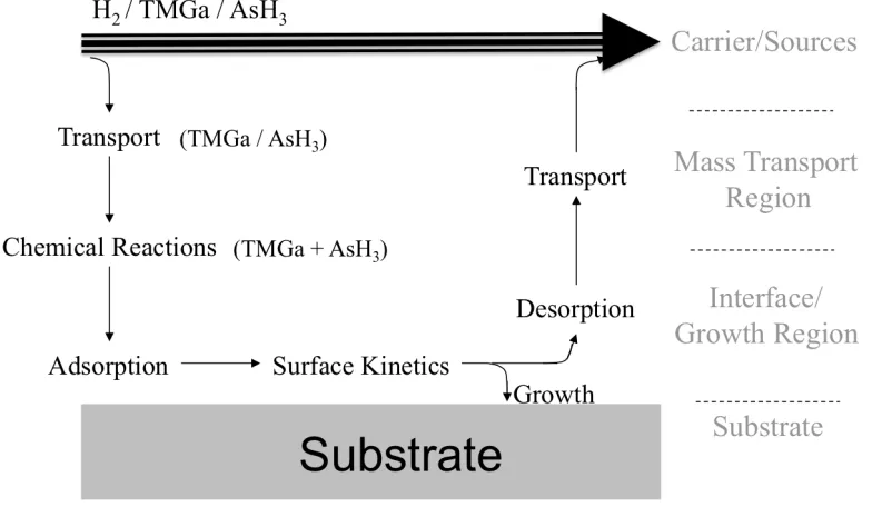
The CVD process involves four regions; they are the substrate, interface/growth,
transport and carrier/source regions. The series of steps in the CVD process for
epi-taxial growth of GaAs is illustrated in figure 1.1. The gasses containing the required
[image:19.612.125.517.360.588.2]source elements flow into the chamber from the left, as seen in the figure.
Figure 1.1: Schematic of OMVPE process.
interface regions, which causes diffusion of these molecules toward the substrate
sur-face. The precursor molecules then undergo pyrolysis, whereby TMGa experiences
homogeneous decomposition of methyl groups and AsH3 experiences breaking of the
hydrogen bonds. Ga and As then adsorb to the substrate where the individual species
react kinetically to form the desired GaAs according to the chemical reaction given by
AsH3+ (CH3)3Ga−→GaAs+ 3CH4 (1.1)
The precursor molecules are constantly supplied throughout the OMVPE process,
however, at high growth temperatures, desorption occurs, as illustrated in figure 1.1.
Because of this, the growth of compound semiconductor material by OMVPE requires
an overpressure of the group V material, like AsH3, to prevent the decomposition of
material at the substrate. The organic by-products such asCH4 are transported from
the interface region to the carrier gas and expelled from the reactor chamber as waste.
GaAs was one of the earliest materials to be developed by OMVPE and offers
several advantages over silicon, which dominates the photovoltaic industry. GaAs,
and many other III−V materials, have a direct bandgap, compared with the indirect
bandgap of silicon. This allows for the direct absorption of photons, leading to stronger
absorption for GaAs over Si. Stronger absorption means that GaAs devices can be
made thinner since most of the sunlight is absorbed within ∼ 2−3µm. This saves
material cost and weight, which is an important factor for consideration when using PV
devices in space. GaAs devices have also demonstrated improved radiation tolerance
experienced by satellites outside of shielding from the earth’s magnetic field.
The potential selection of materials for device application was greatly expanded
with the advent of OMVPE technology. The material system was extended from single
compound materials to a wide range ofIII−V materials based on binary and tertiary
compounds of Ga, In, Al, N, P, As and Sb, which could be grown epitaxially. Since
OMVPE allows for abrupt layer growth, the precise deposition and alloy compositions
of these III −V compounds could be controlled, altering the bandgaps and thus,
their electronic and photonic properties. Figure 1.2 is known as the crystal grower’s
chart and displays a variety of III −V compounds with their bandgaps and lattice
[image:21.612.143.498.369.618.2]constants [14].
The plot gives some information on how alloying of different group III and V
el-ements affects the bandgap of the compound as well as giving lattice constant
in-formation for different III −V binaries and tertiaries. Lattice constant is important
when stacking epitaxial layers of different material since lattice mismatch can lead to
strain-related defects. The figure outlines the lattice-matching condition for a state of
the art triple junction solar cell with an (In)GaAs middle cell and InGaP top cell
lattice-matched to the lattice constant of a Ge bottom cell, shown by the dashed box. This
will be discussed in more detail in the next section, dealing with multijunction solar cell
devices grown by OMVPE.
1.3
III-V PHOTOVOLTAICS: SINGE AND MULTI-JUNCTION
1.3.1 Single-Junction GaAs Solar Cell Operation
The difference in energy between the CB and the VB is known as the bandgap (Eg)
and in order to excite a charge carrier from the valence band to the conduction band
for use in a circuit, energy at least equal toEg must be supplied. GaAs has a bandgap
of1.42eV which corresponds to a wavelength of∼870nm. This means that an incident
photon of energy 1.42eV will successfully excite an electron to the CB for collection.
The sun, however, outputs a broad spectrum of wavelengths which closely matches
the spectral irradiance of a 6000K blackbody. A consequence of the single bandgap
of GaAs (or any single bandgap solar cell) and the spectral range of the sun is shown
Ephoton < Eg and Ephoton > Eg. Illustrated in the figure are two intrinsic loss
mecha-nisms for a solar cell. WhenEphoton < Eg (red), the incident photon does not possess
sufficient energy to excite an electron across the bandgap. As a result, the device is
transparent to the photon and it passes through the cell. This is called transmission.
Figure 1.3: Energy band diagram of ap-njunction solar cell showing absorption (green), transmission (red) and thermalization (blue).
The second intrinsic loss depicted in figure 1.3 is the case where Ephoton > Eg
(blue). For these high-energy photons, excitation to the CB occurs, but the electron is
in a higher CB energy state initially and must relax to the band edge in order to
mini-mize its energy. This causes the excess energy to be given off as heat through lattice
vibration or phonons and is called thermalization. Altogether, about 55% of incident
solar power is not usable by a PV device due to thermalization and transmission [15].
intrinsic loss such as Boltzmann loss [16], a landmark paper published in 1961 by
William Shockley and Hans Queisser reported the maximum theoretical efficiency for
a single bandgap solar cell device based on a detailed balance calculation [17].
De-tailed balance is a principle which states that any body which absorbs energy (light)
must also emit energy. Since a photovoltaic device emits more light when optically
ex-cited due to radiative recombination, the power conversion efficiency of the cell is
lim-ited [18]. Shockley and Queisser found that, under thermodynamic balance, the
maxi-mum attainable efficiency under one-sun illumination was 33.1% and corresponded to
a bandgap of∼1.1eV, the bandgap of silicon. This limit became fundamental in solar
cell production and is known as the Shockley-Queisser limit. Despite the maximum
ef-ficiency of33.1%for a silicon cell, modern state-of-the-art single crystal silicon devices
perform at around 24%under one-sun illumination [19, 20]. Due to the direct bandgap
of GaAs and its strong photon absorption along with various PV advances such as
photon recycling, world record single junction devices have been reported, performing
at28.8%efficiency [21], coming close to the theoretical maximum.
1.3.2 Multi-junction Solar Cells
Single bandgap photovoltaic devices are limited in their ability to effectively convert a
wide range of the solar spectrum into usable energy due largely to loss by transmission
and thermalization. There have been several attempts to increase power conversion in
PV devices in recent years, one of which is the multi-junction solar cell [22]. The
materials of different bandgap, each electrically connected by tunnel junctions. The
wider bandgap materials at the top of the stack serve to filter the shorter wavelength
light by absorption while less energetic photons pass through to the lower junctions
whose bandgaps are more sensitive to those wavelengths. With appropriate selection
of materials, this structure reduces the loss due to thermalization as well as
trans-mission, leading to higher power conversion efficiencies. The current state-of-the-art
triple junction solar cell (TJSC) design is shown in cross section in figure 1.4. This
type of device consists of a Ge bottom cell (Eg = 0.70eV), an (In)GaAs middle cell
(Eg = 1.4eV) and an InGaP top cell (Eg = 1.8eV) connected by tunnel junctions as
shown to the right of the figure.
Figure 1.4: Left: Absorption of each layer in the TJSC compared with the AM0 solar spectrum. Right: Cross section of a state-of-the-art triple junction solar cell.
To the left of figure 1.4, a plot of theAM0solar spectrum is shown, overlaid with the
power conversions of each junction in the TJSC device, calculated by detailed balance.
and the spectral irradiances of the junctions, but compared with a single-junction GaAs
device (here, the middle junction), its effect is reduced. Also, the absorption of the
TJSC has been extended to ∼ 1.7µm by the inclusion of the Ge junction, compared
with the absorption cutoff of0.87µmfor the single junction GaAs device. Thus, loss due
to transmission is reduced by the use of multiple junctions. Modern TJSC devices have
been reported performing at around 33% efficiency under one-sun illumination [23].
The selection of materials with appropriate bandgap is important when designing
a multi-junction solar cell device, however, a major constraint when selecting the
ma-terial system is the lattice-matching condition. Growth of mama-terial by epitaxy can be
either strained, by lattice-mismatching the epilayer and the substrate or not strained,
by lattice-matching the epilayer to the substrate. Lattice-mismatching, or growth of
material with a different lattice constant than the substrate leads to strain-related
de-fects, such as misfit dislocations, which degrade the performance of the device. Thus,
the material system for the multi-junction solar cell shown in figure 1.4 is limited by the
single lattice constant of the Ge substrate, which was illustrated in figure 1.2.
A second constraint which limits the performance of a TJSC is the current-matching
condition. Since the three sub-cells are connected in series, the current through each
cell must be constant. For this to be true, the entire device must output current equal
to the smallest sub-cell current. Integration of the sub-cell responses in figure 1.4
indicates that the GaAs junction is the current-limiting junction in the TJSC shown.
Since output power is the product of current and voltage, in order to produce more
but the change in voltage of the device is less dramatic, since in a series circuit, the
voltage across each resistive load adds. Unfortunately, the lattice-matching condition
makes the selection of different materials difficult without introducing unwanted strain
in the device.
There have been several proposed methods to improve device efficiencies beyond
33%. Some of these include growth of four and five junctions [24, 25] which further
increase absorption and reduce intrinsic loss in the device. The challenge which
exists for inclusion of more junctions is the lattice-matching constraint which makes
the growth of material with both an appropriate bandgap and lattice constant difficult.
However, Y. Masafumi et al. and others have reported theoretical device efficiencies
for four-junction devices of over40%under one-sun illuminations [24]. Another method
is the inverted metamorphic (IMM) solar cell design which allows the growth of
lattice-mismatched materials whose bandgaps are closer to the ideal bandgap for a
multi-junction device with bottom-cellEg = 1.0eV [26]. Such devices have been reported to
perform with40.7% efficiency under a concentrated terrestrial spectrum [27].
Another method for improving device efficiency, which is the focus of this work,
is known as bandgap engineering. Bandgap engineering is a method by which the
effective bandgap of a sub-cell in the TJSC stack is altered through the inclusion of
nanostructures such as quantum wells (QWs) or quantum dots (QDs), without
affect-ing the lattice-constant, thereby increasaffect-ing the sub-cell current, and thus the overall
device performance. Essentially, by lowering the bandgap of the subcell, its absorption
bottom cell. This would result in a higher matched current through each subcell and
thus a higher output power from the device. Quantum dot bandgap engineering has
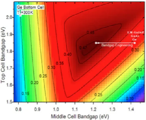
been extensively investigated at RIT in recent years [28]. Figure 1.5 shows the result
of a detailed balance calculation as a contour plot indicating the efficiency for a TJSC
with a Ge bottom cell and varied top and middle cell bandgaps. The x-axis represents
the varied bandgap for the middle cell and the y-axis represents the varied bandgap
[image:28.612.181.457.291.519.2]for the top cell. The contour lines are those of constant efficiency.
Figure 1.5: Contour plot of efficiency versus top cell and middle cell bandgap for a TJSC structure with fixed Ge bottom cell indicating benefit of bandgap engineering.
The figure indicates the power conversion efficiency of33% for the TJSC structure
shown in figure 1.4 corresponding to a middle cell bandgap of 1.42eV and a top cell
bandgap of 1.85eV. The plot shows, however, that a lower middle cell bandgap can
detailed discussion of nanostructures is made in the next section as well as in the next
chapter on quantum dots.
1.3.3 Nanostructured Photovoltaics & Intermediate Band Solar Cells
As discussed in the last section, the lattice-matched TJSC design is limited in its
effi-ciency by the GaAs current-limiting junction, but through bandgap engineering, current
through this junction and thus the overall power output by the device can be increased.
Bulk materials are only effective absorbers of light up to the band edge, whereafter, a
sharp cutoff in absorption exists and the device becomes transparent to less energetic
photons. The inclusion of a narrow bandgap material in the bulk material can extend
its absorption to longer wavelengths to convert more of the solar spectrum into usable
energy.
In 1972, while working at Bell Labs, Charles H. Henry proposed that the inclusion of
very thin heterostructures (quantum wells) could lead to quantum confinement of
elec-trons and thus, states within the bandgap of the host material. In 1973, Henry’s design
for a double heterostructure was demonstrated by showing sub-bandgap (Ephoton <
Eg) absorption peaks and subsequently the investigation into nanostructured
opto-electronic devices began [29]. The first quantum confining structures were used in the
investigation of quantum well lasers, but in recent time, quantum well and quantum dot
inclusion in solar cell devices has gained popularity as a method for increasing current
output for multi-junction solar cells as well as the realization of the intermediate band
strong coupling of quantum dot states leading to the strong spatial overlap of electron
wave function for the formation on an intermediate energy band within the bandgap
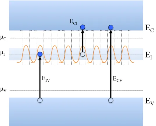
of the host material. A simplified energy band diagram for an IBSC is presented in
figure 1.6. The figure shows the valence and conduction bands along with an
inter-mediate energy band within the bandgap of the host material. The figure indicates
valence band to intermediate band transitions (EIV), intermediate band to conduction
band transitions (ECI) and valence band to conduction band transitions (ECV) as well
[image:30.612.186.454.310.526.2]as the chemical potentials for quasi fermi levelsµV,µI andµC.
Figure 1.6: Energy band diagram for an intermediate band solar cell indicating valence band to interme-diate band transitions (EIV), intermediate band to conduction band transitions (ECI) and valence band
to conduction band transitions (ECV).
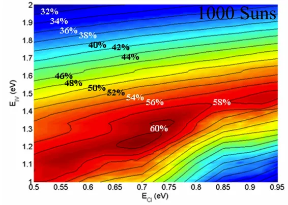
The IBSC device design has been proposed to far exceed the performance of even
multijunction devices [31–33]. Figure 1.7 shows the result of a detailed balance
represents varying the intermediate band to conduction band energy (ECI) and the
y-axis represents varying the intermediate band to valence band energy (EIV). The
plot indicates that under a concentrated terrestrial spectrum, an IBSC exhibits a
maxi-mum theoretical efficiency of over60%compared with33%predicted by Shockley and
[image:31.612.176.459.226.428.2]Queisser.
Figure 1.7: Detailed balance efficiency plot for an IBSC under 1000 sun concentration.
The focus of the work in this thesis is largely the control of QD properties such as
size, shape and ordering through careful control of growth parameters in the OMVPE
reactor for the eventual realization of an IBSC device. Additional motivation for this
work is the theoretical benefit of bandgap engineering, shown in figure 1.5. Presented
in this thesis is an investigation of the benefit of quantum dot inclusion in GaAs solar
cells for current enhancement as well as their inclusion in the GaAs junction of a
state-of-the-art TJSC device for improved power conversion efficiency. A more detailed
1.4
ORGANIZATION OF WORK
The following chapters of this thesis focus on the growth and characterization of InAs
quantum dots by OMVPE as well as the characterization of quantum dot enhanced
single and multijunction III−V solar cells. Chapter 2 is an experimental procedures
chapter, focusing on the underlying and operational principles of the characterization
techniques used throughout this thesis. It should serve as a technical report and does
not present any material or device results. Chapter 3 focuses on the
characteriza-tion of OMVPE grown InAs quantum dots in a small-area Veeco P125LDM reactor at
the NASA Glenn Research Center for the realization of an IBSC. A discussion of the
motivation and theory of nanostructure physics is presented in chapter 3 along with
morphological and optical results for quantum dots grown with different growth
param-eters and device results for quantum dot enhanced single junction GaAs solar cells.
Chapter 4 focuses on the optimization of InAs quantum dot growth in a large-area
OMVPE reactor as well as the characterization of quantum dot enhanced double and
triple junction solar cells. Chapter 5 presents conclusions for both small and
large-area reactor quantum dot growth, solar cell performance as well as a discussion on
Chapter 2
Experimental Procedures
The characterization of samples investigated in this study is separated into two
cate-gories. They are a) characterization of InAs QD test structures grown on GaAs
sub-strates to determine the effect of varying OMVPE growth parameters and b)
character-ization of QD enhanced single and triple junction solar cells with similarly grown QDs
to quantify their effect on solar cell performance. Thus, the testing apparatuses and
methodologies used herein satisfy two purposes: materials characterization for InAs
QD test structures to quantify QD statistical, optical, morphological and bulk
proper-ties, and solar cell device testing to extract performance parameters. This chapter
will serve as the generic basis for all of the testing methodologies used as well as to
provide a technical description of the operating principles behind the measurement
2.1
MATERIALS CHARACTERIZATION METHODS
2.1.1 Atomic Force Microscopy
The main method for quantifying changes due to growth processes is to directly
ob-serve and measure the features grown. While it is possible to get in-situ
measure-ments of the surface during MBE growth using techniques like reflection high-energy
electron spectroscopy (RHEED) [34,35], obtaining similar measurements during MOCVD
growth is slightly more difficult, and so a post-growth method is typically used in
or-der to make direct measurement. Directly accessing structural information of features
is essential to the understanding of the growth process and microscopy is typically
used to observe morphological properties. However, when the size of the features is
extremely small, optical microscopy becomes quickly insufficient for their direct
obser-vation. This is the case for quantum dots, whose size is on the nanometer scale.
In 1986 at IBM, Binnig, Gerber and Quate invented the atomic force microscope
(AFM) which was based on the technology previously used in the scanning tunneling
microscope (STM) [36]. A benefit of the AFM over STM is that the sample surface
does not need to be conducting, and thus AFM has a different range of applications.
AFM is a scanning probe microscopy (SPM) technique, the basic operating principle
of which relies on Van der Waals and atomic forces between an atomically fine probe
tip, usually with tip radius of a few nanometers, and the sample surface.
There are two primary modes of operation for an AFM, contact mode and tapping
its vertical deflection is measured, tracking the contours of the surface. Near the
surface, the short-range attractive forces are very strong, and thus the contact mode
is preferred to a non-contact mode where strong attractive forces cause the cantilever
to snap-in to the surface. In contact mode AFM, the force between the probe tip and
the surface is kept constant by maintaining a constant cantilever deflection, controlled
externally by an electronic feedback loop. From the movement of the cantilever, a
topographical map of the surface is generated which is a digital image of the sample
surface.
The second operational mode, which is the method used in this work, is known as
the tapping mode. This technique is quite similar to operation in the contact mode with
the difference being that the cantilever oscillates very close to its resonant frequency,
typically in the tens to hundreds of KHz range, above the sample surface. This
oscilla-tion produces a laser strip which is reflected by a mirror onto a double-photodetector
array. A schematic of an AFM operating in the tapping mode is shown in figure 2.1.
The array is calibrated so that VA −VB = 0. When a feature on the sample
sur-face is encountered by the tip, the oscillations are dampened due to Van der Waals
forces or other close-range forces, or enhanced in the presence of a valley, changing
the detector reading. This change in voltage is fed into the feedback loop as shown
in figure 2.1, which signals the precise elongation or contraction of a piezoelectric
device underneath the sample surface. Based on the contraction or elongation, a
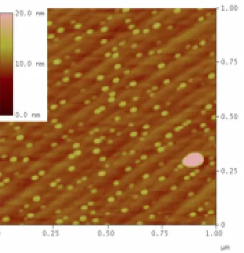
to-pographical image of the sample surface is again generated. A representative atomic
Figure 2.1: Schematic of the operation of an atomic force microscope in the tapping mode.
yellow features distributed throughout being the quantum dots. Evident by the scale
bar inserted in the image, the feature size is typically less than20nm.
Tapping mode AFM is preferred over non-contact AFM since, under normal
am-bient conditions, moisture tends to form in a very thin layer on the sample surface
which makes it difficult to bring the probe tip close enough for short-range forces to
be detectable while preventing the tip from sticking. It is preferred over contact mode
because less damage is sustained by the sample surface and the tip due to the
gen-tleness of operation in the tapping comparatively. Thus, tapping mode AFM can be
used to image very soft materials and results can remain constant over a much longer
time range than is possible in contact mode [37].
For samples in this study, a Veeco D3100 multimode atomic force microscope was
Figure 2.2: Representative atomic force micrograph for samples used in this study.
select scan parameters. For scans presented, the tip used was a Veeco OTESPA
tip was used which provided high lateral resolution. The tip diameter at its finest
point was nominally 10nmwhich was sufficient for imaging nanostructures with lateral
dimension on the order of20−30nmlike those investigated in this work. From the data
collected by AFM measurement, statistical properties such as nanostructure height,
diameter, number density and volume can be extracted using metrology software. For
the work performed for this thesis, Scanning Probe Image Processor (SPIP) software
from Image Metrology was used. SPIP Data from successive experiments is given in
the following chapters where analysis of results is made.
2.1.2 Photoluminescense Spectroscopy
Photoluminescence (PL) spectroscopy is a nondestructive, non-contact method used
photoluminescence provide direct insight into material properties such as the
deter-mination of bandgap, impurity levels and defect detection, and recombination
mecha-nisms. The bandgaps present in a material can be directly measured by PL according
to the wavelengths of photons emitted through radiative recombination of charge
car-riers. A photon’s energy is related to its wavelength according to Ephoton = hc/λ.
A schematic of the radiative and non-radiative processes associated with PL is
pre-sented in figure 2.3. The figure illustrates three processes which make up
photolumi-nescence spectroscopy. They are a) photoexcitation of electrons to the CB by photons
of energy greater thanEg, b) non-radiative relaxation to conduction band edge through
repeated lattice vibrations and c) spontaneous radiative recombination of charge
car-riers. Process (b), illustrated in the figure, occurs quickly, on the order of picoseconds
(10−12s). Process (c) takes place a bit more slowly, in the nanosecond to microsecond
[image:38.612.139.498.449.662.2]range (10−9 −10−6s).
In addition to bandgap determination of bandgaps by PL, low temperature
mea-surements can reveal spectral peaks which are associated with impurities contained
within the host material. Additionally, the intensity of emitted PL is directly related to the
relative amount of radiative and non-radiative events. Since non-radiative processes
are associated with defects and impurities, PL can be used to qualitatively monitor
changes in material quality as a function of growth and device processing conditions.
A block diagram of the test setup used in this work is shown in figure 2.4. A
300W/cm2 Ar+ ion 514nm laser was used for photoexcitation of the sample at room
temperature. A 0.5m HoribaJY iHR320 monochromator with a cooled InGaAs
detec-tor was used to measure signal. In order to ensure accurate PL measurements, the
laser signal was chopped at a rate of167Hz and the monochromator was coupled to a
lock-in amplifier to remove lower-frequency noise. Horiba SynerJY software was used
to record the signal and display PL spectra.
2.2
SOLAR CELL OPERATION & TESTING METHODS
2.2.1 Solar Cell Fundamentals
Fundamentally, a solar cell is p-n junction diode, similar to an LED or transistor. When
the solar cell is illuminated with light of photon energies greater than or equal toEg, an
electron-hole pair (EHP) is generated. After diffusion to the junction, charge separation
occurs due to the built-in electric field. The current injected by the incident light can
Figure 2.4: Schematic of the PL setup used in this work.
potential difference between terminals. The potential difference generates a current
which acts in the opposite direction to the induced photocurrent. This reverse current
is called the dark current and behaves similar to the current characteristic of a diode
with an applied bias. For an ideal diode under forward voltage bias with no illumination
the dark current,Idark, varies according to the ideal Shockley diode equation as
Idark(V) =I0
e
qVapp kB T −1
(2.1)
whereI0 is the reverse saturation current,qis the electronic charge,Vappis the applied
voltage bias, kB is Boltzmann’s constant and T is the absolute temperature in kelvin.
Conventionally, photocurrent is taken to be positive, so the net current through the
cell is the difference between the light-injected photocurrent,IL, and the dark current,
Icell(V) =IL−I0
e
qVapp kB T −1
(2.2)
The point at which no voltage is applied is called the short-circuit condition, similar
to that of an electrical circuit. At short-circuit conditions, the second term in equation
2.3 vanishes and the total current through the solar cell is simply the short-circuit
current, Isc. ThusIL =Isc at short-circuit. Figure 2.5 (left) shows the current-voltage
I−V characteristic for a solar cell under forward bias both in the dark and illuminated.
The effect of the induced photocurrent at the short-circuit condition is that the I −
V curve is shifted into the fourth quadrant by an amount equal to Isc as shown in
the figure. This is known as the power quadrant because it is the operating region
where power is generated. As previously stated, the usual sign convention is that
photocurrent is taken to be positive, so the illuminated diode I −V characteristic is
flipped into the first quadrant to demonstrate that the solar cell is generating power.
This is shown in figure 2.5 (right).
As bias is increased, the diode forward operation current (Idark(V)) begins to
bal-ance out the photocurrent. At a certain applied forward bias, IL−Idark(Vapp) = 0. This
voltage bias point is called theopen-circuit voltage(Voc), similar to that for an electrical
circuit. Voc is indicated on the righthand plot in figure 2.5 as the intercept to the
volt-age axis. The power out of the solar cell can be calculated for any coordinate pair of
voltage and current in the plot shown in figure 2.5 by taking the product of the two. In
other words P = IV. Total power is plotted on the same set of axes in the righthand
Figure 2.5: Left: Example diodeIV curve with and without illumination. Right: Example solar cellI-V curve with example parameters.
power is generated is called Pmax and is given by the product of some current (Imax)
and voltage (Vmax) which maximizes this quantity. This is the operating point for a solar
cell and is indicated at the knee of the power curve in figure 2.5. Fill factor which is
roughly a measure of the squareness of theI−V curve is calculated fromPmaxas the
ratio
F F = Pmax
Isc∗Voc
= Imax∗Vmax
Isc∗Voc
(2.3)
or the ratio of areas of the grey square to the green square illustrated in figure 2.5.
The most important solar cell parameter is the power conversion efficiency.
Ef-ficiency is a measure of the ratio of the work or power output by the device to the
amount of work or power put in by an outside source. Solar cell efficiency, η, can be
η = Pmax
Pin
= Isc∗Voc∗F F
Pin
(2.4)
where Pin for a solar cell is Psun and the normalized irradiance changes depending
on the spectrum to which the cell is exposed. Solar spectra are discussed in the next
section.
2.2.2 Solar Cell Testing Methods
Testing of photovoltaics is done under a well defined standard spectrum, which can
be different depending on the conditions under which the device is to be used. The
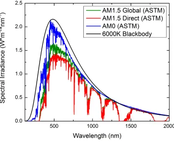
sun’s spectrum closely matches the spectral irradiance of a 6000K blackbody and is
often modeled as such. The solar spectrum changes as the angle of the sun changes
with respect to earth’s zenith. The optical path length that the sun’s light must pass
through is known as the air mass and depending on where and when a solar cell is
tested under an incident solar spectrum, a different air mass value must be used.
Fig-ure 2.6 shows the standard AM0,AM1.5GandAM1.5Dsolar spectra, with a 6000K
blackbody spectrum as a reference. AM0 represents the solar spectrum incident at
the edge of the Earth’s atmosphere, or under zero air-mass. AM1.5 represents the
spectrum with the sun making an angle of 48.2◦ with respect to the Earth’s zenith, or
under 1.5 air-mass. AM0 is the standard spectrum for testing photovoltaic devices
under space conditions and AM1.5 is the standard spectrum for testing devices for
terrestrial application. The dips in the AM1.5spectra shown in figure 2.6 arise due to
of the Earth’s atmosphere, these absorption and scattering effects are not observed.
Figure 2.6: AM0 and AM1.5 solar spectra compared with a6000Kblackbody spectrum.
In order that solar cell testing results be consistent between different labs and
man-ufacturers, a set of standards has been measured by the National Renewable Energy
Lab (NREL) [38] so that solar simulators can be calibrated to whichever spectrum
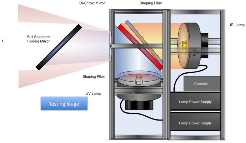
is necessary for a particular test. Samples tested in this work were done using a
TS Space Systems (TSS) dual-source solar simulator calibrated to closely match the
ASTM standard for both AM0 and AM1.5 spectra. A schematic of the solar simulator
iodide (HMI) lamp which provided the visible and ultraviolet part of the spectrum, and
a 12kW quartz-tungsten halogen (QTH) bulb which provided the near infrared (NIR)
and infrared (IR) part of the spectrum. Also shown in the figure are several shaping
filters as well as a dichroic mirror to shape and combine the spectra of the two lamps.
A plane full spectrum folding mirror was used to direct the combined spectrum toward
[image:45.612.99.508.280.518.2]the sample stage for illumination of the device under test.
Figure 2.7: Block diagram of TS Space Systems solar simulator at RIT.
The two lamps were calibrated underAM0conditions using an InGaP2and a GaAs
reference cell provided by NASA Glenn Research Center. The InGaP2 reference cell
was used for calibration of the HMI lamp since the cut-on wavelength of the QTH
calibrate the QTH lamp due to its strong response in the NIR region of the spectrum. A
calibrated TSSAM0spectrum is shown in figure 2.8 overlaid with the ASTM standard
AM0 spectrum. The spikes in the TSS spectrum, shown in the figure, can be further
smoothed by the inclusion of additional filters in the system, but it is clear that the two
[image:46.612.139.496.230.512.2]spectra are a close spectral match.
Figure 2.8: TSS simulatedAM0compared with the ASTM standardAM0spectrum.
2.2.3 Spectral Responsivity and Quantum Efficiency
An key parameter when characterizing a solar cell’s performance under different test
conditions is the cell’squantum efficiency(QE). QE(E)is a measure of the probability
strength of QE as a metric for solar cell device and material characterization is that it
does not depend on the incident spectrum. Instead, it depends the absorption
coef-ficient of the solar cell material, the efficiency of charge separation and the efficiency
of charge collection in the device [18]. Thus, QE is directly related to the solar cell
material quality and device design.
Detailed balance calculations predict device performance for a given set of test
conditions, but make several assumptions to simplify the model, for example, that
every incident photon creates a charge carrier for use in the circuit. In an actual
device, not every incident photon results in a collected charge carrier, so the QE is
rarely equal to unity at any specific wavelength. QE can be either directly measured
or modeled in terms of the solar cell device’s spectral responsivity (SR), which is a
measure of the amount of current (A) per unit power (W) illuminating the device at a
given wavelength, λ. A was model developed by H. Hovel and J. Woodall [39] based
on a series of carrier transport equations which can be used, along with absorption
data for a material to model current collection in a device. External quantum efficiency
(EQE), which is the ratio of collected charge carriers to the number of incident photons
of a given energy can calculated from measured SRas
EQE(%) =SR∗ hc
qλ (2.5)
where SR is the cell’s spectral responsivity at a particular wavelength, h is planck’s
constant, c is the speed of light in a vacuum, q is the electronic charge and λ is the
Figure 2.9 shows, as an example, the spectral responsivity, reported as external
quantum efficiency for a bulk GaAs p-i-n solar cell. The dotted line in the figure
rep-resents the band edge of GaAs at 870nm. As discussed in chapter 1, bulk materials
are only effective absorbers of light up to the band edge, whereafter a sharp cutoff
in absorption exists. This is illustrated in figure 2.9 with a sharp decrease in spectral
responsivity for GaAs. At wavelengths beyond 870nm, very little to no incident light
causes any current out of the device. The GaAs device is transparent to photons of
[image:48.612.141.494.319.587.2]longer wavelength than λg,GaAs.
Figure 2.9: External quantum efficiency for a GaAsp-i-nsolar cell device.
SR can also be used to calculate a solar cell’s short circuit current under any
required and in order that the data be reliable, the simulator must have a low degree
of spectral mismatch from the lamps and filters used to create the spectrum.
How-ever, solar spectrum data is available for a wide range of different conditions. Using
this available data, and the measured SR of the solar cell, Isc can be calculated by
integrating theSR convolved with whichever spectrum is appropriate for the test
con-ditions. IntegratedIsc is calculated as
Isc =
Z λ2
λ1
SR(λ)∗φspectrum(λ)dλ (2.6)
where SR(λ) is the measured spectral response and φspectrum(λ)is the desired solar
spectrum.
Figure 2.10 gives a block diagram of the test setup used for SR measurements in
this thesis. SR is measured using an Optronics Laboratories (OL) 750
monochroma-tor, an optical chopper, a lock-in amplifier and source meter as shown in the figure. A
tungsten bulb provides the required spectral bandwidth and diffraction grating is used
to step through wavelengths for solar cell illumination at desired increments. Due to
low signal intensities, an optical chopper coupled to a lock-in amplifier is used in order
to provide noise-free amplification of the output signal. The solar cell is held at
short-circuit current conditions and illuminated in order to measure the response for a given
wavelength. Results are then normalized to a calibration run in order to accurately
Chapter 3
Quantum Dot Growth on 2” Gallium Arsenide
Substrates
3.1
NANOSTRUCTURES IN PHOTOVOLTAICS
3.1.1 Theory
Nanostructures, such as quantum wells (QW), quantum wires (QWR) and quantum
dots (QD) are structures with at least one dimension on the nanometer (10−9m) scale.
Their size in this dimension is on the order of the de Broglie wavelength of an
elec-tron in that material (40nm for bulk InAs [40]), resulting in quantum confinement in
that dimension. Quantum confinement of electrons (and holes) leads to a change in
the density of available states in the material which has a pronounced effect on the
electronic properties of the structure. Figure 3.1 shows the density of states versus
energy for a bulk material and then the varying degrees of quantum confinement for
each type of nanostructure with electron movement confined to two dimensions for a
the density of states function shifts from a parabolic shape in the bulk material to a
more discrete or atom-like set of states for the QD.
Figure 3.1: Density of states for bulk material as well as for nanostructured materials.
QWs, QWRs and QDs are used in lasers, photodetectors and solar cells due to
their tunability of optical and electronic properties [41]. A benefit of the inclusion of
indium arsenide (InAs) QDs in the host material of a solar cell, such as GaAs is that
their narrower bandgap (0.35eV for bulk InAs compared with 1.42eV for GaAs) allows
lower energy photons which could not previously be absorbed, to now be absorbed
by the QD layer and a secondary photon can excite the electron into the conduction
band for current collection. Furthermore, carriers can escape the QD potential by
tunneling or by thermal escape which was not possible for a device without QDs.
for PV devices [42, 43].
The typical design for a QD enhanced solar cell is to include the QDs in the intrinsic
or undoped region of a p-i-n structure device. The band structure of such a device is
shown in figure 3.2, illustrating the secondary escape mechanisms for a carrier in a QD
state. Recall that previously (figure 1.3), the low energy (red) photon was transmitted
through the solar cell and current was lost as a result. Thus, the inclusion of InAs QDs
can extend the absorption of a GaAsp-i-n solar cell.
3.1.2 Quantum Dot Self-Assembly
In this study, InAs quantum dots were grown by OMVPE at the NASA Glenn Research
Center (GRC). InAs growth is similar to the growth of GaAs, given by equation
Equa-tion 1.1, with trimethylindium (TMIn) as the groupIII precursor, as opposed to TMGa.
InAs QD growth occurs at lower temperature than GaAs growth (470◦Ccompared with
600◦C) due to the high mobility of the indium species. Growth temperatures too high in
excess of500◦Ccan result in the desorption and dissolution of InAs from the substrate
surface [44].
There are several types of heteroepitaxial growth modes, each resulting from
dif-ferent interfacial energies and substrate mismatches. Some of these are Frank-Van
der Merwe (FW), or layer-by-layer growth, Volmer-Weber (VW), or 3D island formation,
and Stranski-Krastanov (SK), or wetting layer to 3D island growth [45]. Equation 3.1
gives the condition for layer-by-layer growth to occur as
∆γ =γA+γi−γB ≤0 (3.1)
whereγAandγB are the surface free energies of species A and B respectively, andγi
is the interfacial free energy.
FW growth (2D) occurs in systems where the energies of the epilayer and
inter-face sum to a lower energy than the substrate, in other words, the deposited
mate-rial and substrate matemate-rial are lattice-matched and equation 3.1 is satisfied [46]. In
(3D) occurs in systems whose epilayer and interface energies sum to a greater
en-ergy than the substrate. In other words the deposited material and the substrate are
lattice-mismatched. VW growth occurs in systems which the lattice constant,a, of the
epilayer and the substrate are highly lattice-mismatched (aepi/asub >10%) resulting in
strain-induced 3D island formation as well as plastic deformation of the crystal,
result-ing in a high density of interfacial misfit dislocations [47]. The SK growth mode is an
intermediary type of growth, characterized as a 2D to 3D type of growth [48] and is the
growth method of QDs in this study.
SK growth occurs when the substrate and deposited material are slightly (<10%)
lattice-mismatched. For an InAs/GaAs material system, a 7.2% mismatch exists. In
these systems, monolayers (half of the lattice constant, ∼ 3A˚ for InAs) of InAs are
grown directly on the substrate where the larger-lattice-constant InAs molecules
com-press so that their lattice constant matches that of the GaAs substrate below, thus
compressively straining the epi-layer. This, however can only occur for very thin layers
of InAs as strain continues to increase throughout the deposition. At a certain InAs
layer thickness, θc, called the critical thickness, deposition of more InAs results in a
change from adhesion of material to the substrate to cohesion of adsorbed molecules.
Through this process, the InAs molecules volumetrically relax to their natural lattice
constant and newly deposited InAs bonds preferentially to the newly formed clusters
as it is more energetically stable. The end result is the formation of coherently strained
3-D islands which are called quantum dots. The SK growth process is shown
Figure 3.3: 2D FM Growth mode (top row), 3D VW growth mode (middle row) and 2D to 3D SK growth mode (bottom row) with increasing deposition.
The process outlined in figure 3.3, however, doesn’t truly represent the structure
depicted in figure 3.2 which shows multiple potential wells, or quantum dots in the i
region of ap-i-ndevice. Figure 3.3 can be thought of as the process for growing each
layer individual layer of QDs, but typical optoelectronic application usually requires the
growth of a stack of QD layers for electronic coupling and signal amplification [49].
The growth of a stack requires careful considerations in the growth process, outlined
3.1.3 Stacked QD Layers & GaP Strain Compensation
The growth of multiple layers of InAs QDs in a GaAs host requires the growth of GaAs
spacer layers between InAs layers. The thickness of the spacer is typically only a few
nanometers and is split into low temperature (LT) GaAs and high temperature (HT)
GaAs layers. LT GaAs is grown at the same temperature as the QD layer and serves
to cap the QDs, preventing dissolution of InAs as temperature is later increased. GaAs
grown at this low temperature tends to be lower crystal quality material. The HT layer
is then grown and acts as the GaAs surface on which the next layer of QDs is grown.
This layer is grown at high temperature to maintain good crystal quality in that layer.
InAs growth on GaAs, however, leads to compressive strain in the InAs layer and
growing multiple layers in the InAs/GaAs system leads to the buildup of strain through
the structure and eventually results in the formation of dislocations.
A method proposed by Hubbardet al.[50] to mitigate the build-up of compressive
strain in order to grow multiple layers of defect-free InAs QDs on GaAs is to grow
a thin layer of GaP between spacer layers. The lattice constant of GaP is a 3.6%
tensile mismatch to that of GaAs (compared with the 7.2% compressive mismatch
for InAs/GaAs). The thickness of the GaP layer must be carefully controlled in order
that tensile strain effectively compensates the compressive QD strain. A modified
continuum elastic theory (CET) model was developed by Baileyet al.to determine the
thickness of the GaP layer for a given density and size of quantum dots, that results
in the minimum overall superlattice stress [51]. This led to an optimum GaP thickness
quantum dot enhanced solar cell (QDSC) short-circuit current over a baseline device
and to improve power conversion efficiency of a QDSC compared to a device without
strain compensation [52]. Figure 3.4 shows a comparison of an InAs QD stack in a
GaAs host with and without strain compensation. On the left of figure 3.4, a strained
QD superlattice stack is shown, with non-uniformity in the individual layers and some
visible threading dislocations shown near the upper left corner of the image. These
types of dislocations arise due to the strain from InAs growth on GaAs. To the right
of the figure, a similar stack of QDs is shown with a GaP strain compensation layer.
This stack shows more uniformity in the QD layers, compared with the uncompensated
stack on the left and did not exhibit any threading dislocations.
Figure 3.4: Transmission electron micrographs of an InAs QD stack with no strain compensation (left) and GaP strain compensation (right).
The OMVPE process flow for SK grown InAs QDs in a GaAs host is shown
schemat-ically in figure 3.5 as a temperature and flow versus time plot. Figure 3.5 shows the
stage on the bottom. At the second stage shown, the temperature is ramped down
to facilitate the growth of the InAs QD layer followed by a LT GaAs layer. The
tem-perature is then ramped up for HT GaAs growth and a HT GaP strain compensation
layer, followed by another HT GaAs buffer layer. This process is then repeated until the
desired number of QD layers is grown, when the temperature is ramped down under
[image:59.612.143.499.280.569.2]AsH3 ambient.
3.2
MATERIALS RESULTS
Test structures grown for materials characterization consisted of a300nmthickn-type
GaAs buffer layer grown at 620◦C followed by a 5-period superlatti
![Figure 1.2: Bangap energy vs. lattice constant for common III-V semiconductors. [14]](https://thumb-us.123doks.com/thumbv2/123dok_us/45840.4145/21.612.143.498.369.618/figure-bangap-energy-lattice-constant-common-iii-semiconductors.webp)