Rochester Institute of Technology
RIT Scholar Works
Theses Thesis/Dissertation Collections
2012
The Impact of polarization on the performance of
all-optical flip-flops
Claudio Ippolito
Follow this and additional works at:http://scholarworks.rit.edu/theses
This Thesis is brought to you for free and open access by the Thesis/Dissertation Collections at RIT Scholar Works. It has been accepted for inclusion in Theses by an authorized administrator of RIT Scholar Works. For more information, please [email protected].
Recommended Citation
The Impact of Polarization on the
Performance of All-Optical Flip-Flops
by
Claudio E. Ippolito
Submitted in Partial Fulfillment of the Requirements for the Degree of
Master of Science in Telecommunications Engineering Technology
Supervised by
Drew Maywar, Ph.D.
College of Applied Science & Technology
Electrical Computer and Telecommunications Engineering Technology
Rochester Institute of Technology
Rochester, New York
To God, my family and my dearest friends:
Never have I been more grateful of your support, kindness and
wisdom than in this moment
I owe it all to you
To my Nonna Gilda, Nonno Luigi and my Tío Ricardo y Alberto:
Always by my side
“All life is an experiment. The more experiments you make the better.”
Abstract
The Impact of Polarization on the Performance
of All-Optical Flip-Flops
Claudio E. Ippolito
Acknowledgements
(goes in no particular order)
Words fall short to express my deepest gratitude to Dr. Drew Maywar, my research advisor, mentor and friend. In more than one occasion prior to engaging in this 9-month task I told him about my concerns of doing research. How could it be that I can contribute to science? I clearly did not have the academic or professional background for pursuing such an ambitious goal.
Drew not only gave me the confidence to pursue a thesis, with his support and guidance this nightmare-prone scenario became perhaps my most rewarding educational and personal experience ever. Drew took the time to teach me all the do’s and don’ts of working in a photonics lab and in just 2 months, I was confidently on my own, amongst experimental equipment that are the dream and envy of many institutions worldwide. In 9-months I have learned invaluable skills, both professional and personal that I am never going to forget.
Rie and his two wonderful, full of life children Ian and Anna, all this while experiencing amazing homemade Japanese food.
I’m truly very lucky and I’m going to miss our weekly meetings where I said so many out-of-the-hat theories and Drew, calmly and patiently, pointed me in the right direction. Phrases like “ballpark a number” and “don’t spill the beans” are going to stay with me dearly forever.
I would like to thank my entire family for supporting me during my education. It is only because of you that I have reached this moment. You made me what I am and every day I am thankful for being born in the family that through the years, and with all its mistakes, has showed me that it is the best family in the world. Every day I woke up fantasizing about the moment where I could give you the final copy of my work. This moment is now only two weeks away. You are my most precious possession on this universe, I love you all.
Table of Contents
I. Introduction 1
I.1 All-Optical Flip-Flops (AOFFs) 1 I.2 Motivation & Scope of Thesis 4 I.3 Semiconductor Optical Amplifiers (SOAs) 5
I.3.1 Types of SOAs 6
I.3.2 SOA Nonlinearities 7 I.4 EM Waves & Polarization 8 I.4.1 Stokes Parameters and the Poincaré Sphere 12
II. Investigation of the Bistable Hysteresis 15
II.1 Shift of the Longitudinal Modes 15 II.2 Shift with Injection Current 18 II.3 Shift with Optical Power 23 II.4 Dispersive Bistability 29 II.5 Dependence on Input Polarization 37
III. AOFF Contrast Enhancement via its Input Polarization 48
III.1 Hybrid Control of an AOFF 48 III.2 Impact of Input Polarization 56
IV. AOFF Contrast Enhancement via its Output Polarization 61
IV.1 Demonstration of Contrast Enhancement 64
V. Concluding Remarks 71
VI. Appendix: Tips on using the Polarimeter 73
List of Tables
List of Figures
Figure 1. Basic AOFF operation. ... 3
Figure 2. All-optical packet switch concept system. ... 3
Figure 3. Basic SOA schematic. ... 5
Figure 4. The two main types of SOAs... 6
Figure 5. Poincaré Sphere. ... 13
Figure 6. Dependence of gain and the refractive index on the carrier density. ... 17
Figure 7. Dependence of gain and the refractive index to injection power. ... 19
Figure 8. Experimental setup to study the resonance shift of the RT-SOA by varying the carrier density. ... 20
Figure 9. Resonance shift of the FP-SOA due to different injection currents. ... 21
Figure 10. Peak resonance power and wavelength shift of the longitudinal mode vs. injected current... 22
Figure 11. Dependence of gain and the refractive index to input optical power. ... 23
Figure 12. Experimental setup to study the resonance shift of the RT-SOA by gain saturation. ... 24
Figure 13. Resonance shift of the FP-SOA from different CW optical signal powers. ... 25
Figure 14. Peak resonance power and wavelength shift of the longitudinal mode vs. CW beam power. ... 26
Figure 15. Resonance shifts and gain saturation by increasing signal power. ... 28
Figure 17. Input signal and RT-SOA output as a function of time. ... 31
Figure 18. [a] RT-SOA bistable hysteresis – [b] Zoomed in ... 33
Figure 19. Positive feedback loop that triggers the high bistable state. ... 34
Figure 20. Negative feedback loop that triggers the low bistable state. ... 35
Figure 21. [a] Hysteresis behavior for different injection currents – [b] Zoomed in ... 36
Figure 22. Amplifier axes. ... 37
Figure 23. Poincaré Sphere for an electric field propagating in the TE mode (∆Pol = 0.79°) ... 40
Figure 24. Poincaré Sphere for an electric field not propagating in the TE mode (∆Pol = 66.25°) ... 41
Figure 25. Spherical coordinates representation of an SOP in the Poincaré Sphere. .. 43
Figure 26. Hysteresis behavior for different input polarizations. ... 44
Figure 27. [a] Hysteresis behavior for different input polarizations – [b] Zoomed in. 45 Figure 28. Evolution of ∆Pol with the polarization rotation of the optical input signal. ... 46
Figure 29. Evolution of the hysteresis contrast and the upward-switching threshold as ∆Pol increases. ... 47
Figure 30. Hybrid controlled RT-SOA based AOFF. ... 49
Figure 31. Set optical pulses. ... 50
Figure 32. Experiment diagnostics setup. ... 51
I.
Introduction
I.1
All-Optical Flip-Flops (AOFFs)
Still today, most optical signals that travel through fiber-optic networks need to be converted to their electrical counterparts to be processed. This conversion is called an OEO (Opto-Electro-Optic) conversion. For example, OEO conversions are done in wavelength switching nodes of a network that lack all-optical wavelength converting capabilities. In these nodes, all the incoming optical data on an optical wavelength must be electrically replicated before it can be converted back to optical signals on a new wavelength.
Switching wavelengths through OEO conversion has some advantages. Since the data must be rebuilt optically, it is going to be regenerated, reshaped, and retimed right away. This seems very attractive as it deals with the long-haul related fiber impairments; however, there is a strong drawback with this approach. OEO conversions are done on a per-wavelength basis and it is a complex and hardware-intensive task, so the equipment is quite expensive. Not only that, usually OEO approaches are also protocol and bit-rate dependent, have a large footprint and power consumption, introduce delays, place throughput bottlenecks, and increase the probability of errors.
network without the inconvenience of doing costly OEO conversion maybe a key to satisfying the exponential growth in data consumption that we are witnessing today.
Signal-processing techniques are largely classified as combinational or
sequential [1]. Combinational techniques are those where the output is a consequence
of the present input. A basic logic circuit that uses combinational processing is a half adder, which does the addition of two bits using AND & OR logic gates. Sequential techniques are those where the output is determined by the present value of its inputs and its past state. A flop is a logic circuit that does sequential processing. A flip-flop has two stable output states that change when one or more signals are applied to its control inputs.
All-optical flip-flops (AOFFs) are important to all-optical sequential signal processing. An AOFF is a device that has a bistable behavior in which both states can
be latched. Once either state is achieved, the device remains in that state until a
specific condition makes it “set” or “reset” depending on its previous condition and the incoming control pulses. This dependence on the previous condition is what gives a flip-flop its so called memory characteristic. There are several ways to achieve an AOFF; one of them is by using semiconductor optical amplifiers (SOA).
“off” state. This type of AOFF will be discussed thoroughly later as it is the one used for the experiments described in this paper.
Figure 1. Basic AOFF operation.
All-optical packet switches are a good example of how AOFFs make all-optical sequential signal processing possible. This all-optical packet switch is comprised of three functional blocks: the all-optical header processing block, the all-optical flip-flop memory block, and the all-optical wavelength conversion block [2] as shown in Figure 2.
Figure 2. All-optical packet switch concept system.
all-optical processing block. Here, the header is translated into an optical pulse that triggers the AOFF to output wavelength or depending of the payload data. This wavelength is then fed into a wavelength converter and is the wavelength of the output
data, avoiding the need to perform an OEO conversion.
I.2
Motivation & Scope of Thesis
AOFFs are key elements in the quest of realizing an all-optical communications network. AOFFs can be achieved in various ways, each one with varying approaches on how to exploit different types of bistability [3-5]. AOFFs such as the one proposed by Maywar, et al. [6] are based on a resonant-type semiconductor optical amplifier (RT-SOA) and show poor on-off switching contrast of around 3 dB (2:1), which is a deterent for using it in commercial systems.
The experiments performed in this thesis map out the dependence of the injected polarization state of an AOFF based on a RT-SOA and clearly show how to optimize the on-off switching contrast to achieve 8 dB. Beyond this optimization technique, a novel technique to achieve an on-off switching contrast exceeding 30 dB (1000:1) is also demonstrated, setting a new contrast record.
hybrid-controlled AOFF based on a RT-SOA. Chapter IV demonstrates a way to achieve an on-off switching contrast of 1000:1, and is again based on the polarization-dependent bistable hysteresis described in Chapter II. Chapter V is dedicated to the concluding remarks of our research. Finally, we share our trials and tribulations in Chapter VI.
I.3
Semiconductor Optical Amplifiers (SOAs)
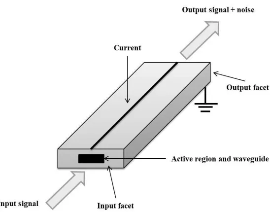
[image:16.595.162.436.372.587.2]SOAs are vital for the AOFF used in our experiments. They are essentially lasers in terms of their physical construction. Figure 3 below shows the basic structure of a SOA.
Figure 3. Basic SOA schematic.
The optical signal travels through a waveguide that confines the signal to the active region. This region imparts gain to the optical signal by means of an external
injection current that provides electrons known as charge carriers. These carriers stay
(VB). When an optical signal is injected, three events happen simultaneously at the photon level: spontaneous emission (that provides optical noise), stimulated emission,
and stimulated absorption.
Stimulated emission is the event of interest for the flip-flop application as it is
the responsible for providing the optical gain that amplifies the optical signal. When a single signal photon has enough energy to cause another photon in the SOA to drop from the CB to the VB, a new photon is created. This photon has the exact same characteristics (phase, frequency, and direction) as the original. Now, these two photons keep on travelling though the semiconductor repeating the process. If there is a high enough external current providing a considerable population inversion of charge carriers, the stimulated emission probability is going to be higher than the absorption probability, and the signal will experience optical gain.
I.3.1
Types of SOAs
SOAs are classified mainly into Resonant-Type SOAs (RT-SOAs) and travelling-wave SOAs (TW-SOAs), as shown in Figure 4. Both types are used in our experiments.
TW-SOAs do not have a resonant cavity, so the optical gain that the beam receives is going to be limited to the amount of charge carriers it can stimulate in a single pass through the device. Reflection from the facets are kept as low as possible (10-4 vs. 0.3 in comparison with laser diodes [7]) as they will produce gain ripples that can severely modulate the amplifier gain and narrow its bandwidth.
RT-SOAs have a resonant cavity that makes optical signals travel back and forth many times. Only the wavelengths that form a standing wave pattern will be reinforced by constructive interference; the others will be suppressed by destructive interference. These constructive wavelengths will provide positive feedback inside the cavity, and they will stimulate the emission of more and more photons on each pass. This stimulation will build up the optical gain of all resonant wavelengths.
A particular type of RT-SOA is a Fabry-PérotSOA (FP-SOA). A FP-SOA is essentially a laser resonator where the resonant cavity has low reflectivity coefficients so its feedback is not high enough to actually make it lase. The FP resonant cavity supports many different standing wave patterns. Each pattern corresponds to different wavelengths that resonate and are going to experience optical gain. These wavelengths are known as the longitudinal modes of the amplifier.
I.3.2
SOA Nonlinearities
SOA nonlinearities are what render our type of AOFF possible. There are several nonlinear effects in SOAs. For our case we are interested in those known as
(XPM), and nonlinear polarization rotation (NPR). They are going to be briefly introduced here, but their effect will be further explained as they happen in the experiments described in later chapters.
Self-phase modulation (SPM) is a nonlinear effect that alters the phase of an optical signal because of changes in the refractive index of the propagating medium. These changes originate from the input signal optical power itself. Cross-gain modulation (XGM) is a nonlinear effect in which the gain experienced by an optical signal is modulated by another co-propagating or counter-propagating optical signals.
Cross-phase modulation (XPM) is another nonlinear effect that also uses a co or counter-propagating optical signal whose power alters the refractive index of the medium, affecting the phase of the other optical signal. Nonlinear polarization rotation (NPR) is the rotation of the polarization state of the SOA output with regard to the input one. The physical cause of NPR is related to SPM & XPM.
I.4
EM Waves & Polarization
are talking about EM waves and their propagation, polarization, shape, working with the wave model is more comfortable.
An EM wave is formed by an electric ( ) and a magnetic ( ) field that travel as a train of plane waves. Both fields are transverse (perpendicular) to the direction of propagation. For the scope of this thesis, we are interested only in the electric field. A general equation to represent an electric field ( ) with a direction of propagation is:
( ) ( ) ( ) 1.1
with
( ) ( ) 1.2
( ) ( ), 1.3
and are unit vectors parallel to the axis of the subscript. The phase offset
between the components is represented by .
Equation 1.2 and 1.3 represent the two perpendicular components of an electric fieldthat varies harmonically as it propagates in the direction.
The orientation of the oscillations of the EM wave in the plane perpendicular to its direction of propagation is the polarization of the EM wave. We care about polarization because some of the components used in this thesis are polarization
sensitive; this means that the transmission, reflection, and/or absorption characteristics
of them vary depending on the state of polarization of the EM waves passing through them.
Different values of account for different polarization states. When is zero or any integer of the waves are in phase. This represents the case of a linearly
polarized wave, which has a polarization vector making an angle with respect to
of:
1.4
with magnitude:
When the phase difference is any general value of the wave is said to have
an elliptical polarization. Rewriting Eq. 1.2 and 1.3 as:
(
) ( ) ( ) ( ) ( )
1.6
yields the general equation of an ellipse. The axis of the ellipse makes an angle relative to the axis determined by:
( )
1.7
Finally, when where and , we have the case of a circularly polarized wave, and Eq. 1.1 becomes:
( ) [ ( ) ( )] 1.8
If the sign is negative, the wave will describe a circle rotating clockwise as it travels on the direction of propagation . This polarization is called right-hand
circular polarization. If the sign is positive, the wave will describe a circle rotating
I.4.1
Stokes Parameters and the Poincaré Sphere
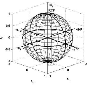
To measure the polarization state of the electric field on our optical signals and how it changes we use the Stokes parameters. The Stokes parameters are a mathematically convenient way to describe the polarization state of an optical signal in terms of its total power ( ) and its degree of polarization (DOP).
They consist of four parameters ( ) that have a straightforward physical interpretation related to the total power of the polarized and unpolarized components of the EM wave. Mathematically:
[ ]
[
( )
( )]
1.10
where:
is the total power of the light (polarized and unpolarized)
describes the preponderance of linear horizontally polarized light (LHP) power ( ) over linear vertically polarized light (LVP) power ( )
describes the preponderance of linear polarized light power forming an angle of 45° (P45) with respect to over linear polarized light power forming an angle
of 45° with respect to (P- 45)
When , , are normalized by , they become ( ). These unitary coordinates represent the state of polarization (SOP) of the signal, and describe a unique point in a Poincaré Sphere like the one shown in Figure 5.
Figure 5. Poincaré Sphere.
This sphere is a convenient graphical way to describe polarization states, because:
Horizontal or vertical linear polarizations (LHP and LVP) are points in the equator with coordinates ( ) respectively.
Linear ±45° polarizations also land in the equator but with coordinates ( ) respectively.
Any other points than these represent elliptical polarizations.
With this 3 coordinates, we can now define and interpret the degree of
polarization (DOP):
√
or
1.11
II.
Investigation of the Bistable Hysteresis
Because RT-SOA nonlinearities are the cornerstone for the type of AOFF used in this thesis, a careful experimental understanding of them is vital before digging into AOFF operation. This chapter presents a series of experiments aimed at characterizing how the nonlinearities that all-together render possible the AOFF respond to changes in their driving parameters such as input power, polarization, and injection currents.
Two types of experiments were performed for this purpose. The first relates to observing the changes in the longitudinal modes to different levels of injection current, which ultimately varies the cavity carrier density. The second type relates to observing the same phenomena but with a fixed injection current and a varying input optical power. This change in optical power will induce gain saturation and ultimately
a bistable hysteresis that will be the basis for optical memory.
II.1
Shift of the Longitudinal Modes
injection current is what provides the charge carriers to the active region to keep on with the stimulated emission process.
The longitudinal modes of an RT-SOA are those wavelengths at which standing
waves are formed inside the resonant cavity, producing positive optical feedback. Mathematically, this happens when the round trip distance of the cavity is integer multiples of the wavelength. If we take half of the round trip (the cavity length), then it must be an integer multiplication of half of the wavelength.
The phase condition to have constructive interference in a Fabry-Pérot cavity
(the type of RT-SOA used for our experiments) is defined as [8]:
2.1
where is the free-space wavelength, the index of refraction of the medium, the length of the resonant cavity, and a positive integer different than zero. Only the wavelengths that correspond to an integer are resonant, and they will be amplified if they are within the gain spectrum. A gain spectrum describes the gain of the amplifier with respect to the wavelength of the modes. Modes that land in this profile are those that will experience optical gain.
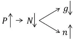
carrier density will shift the location of the resonant modes. Figure 6 and the following equations will help explaining this dependence:
Figure 6. Dependence of gain and the refractive index on the carrier density.
with
( ) 2.2
( ) 2.3
where is the carrier density, is the gain, is the carrier density at transparency, and is the refractive index at transparency. Transparency is the injection current at which stimulated absorption and emission are balanced, providing a net gain of zero.
On the other hand, when the injection current is decreased the carrier density is also decreased. This lowers the gain of the amplifier and increases its refractive index. Increasing the refractive index shifts the longitudinal modes of the resonator to longer wavelengths.
The linewidth enhancement factor is quite useful to explain the variation of the refractive index and gain with the carrier density changes. It is defined as the ratio of the change between the refractive index and the gain with respect to the carrier density in the semiconductor. is expressed as [9]:
( ) ( ) ( ) ( ) 2.4
This expression for if we increase the carrier density by increasing the injection current, the gain will rise while the refractive index will decrease. The linewidth enhancement factor is usually plotted against the energy of the active region bandgap, and it shows how strong the dependence of the refractive index and gain truly is.
II.2
Shift with Injection Current
current, given the refractive index/carrier density relation. As in the previous section, the following figure will help explain this dependence:
Figure 7. Dependence of gain and the refractive index to injection power.
When the injection current is increased the carrier density is increased, thus, the refractive index is lowered and gain is increased. Recalling Eq. 2.1, we can see that lowering the refractive index will eventually shift the longitudinal modes of the resonator to shorter wavelengths.
Figure 8. Experimental setup to study the resonance shift of the RT-SOA by varying the carrier density.
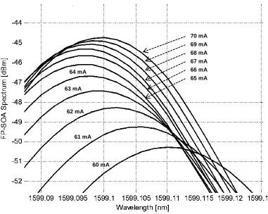
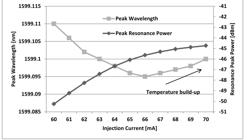
The gain of the longitudinal modes increases constantly as the injection current is raised, as shown in Figure 9. Having more charge carriers available translates into the emission of more photons on each pass, increasing the power of the longitudinal modes.
Figure 9. Resonance shift of the FP-SOA due to different injection currents.
60 mA 61 mA 62 mA 63 mA
64 mA
Figure 10 shows quantitatively how increasing the injection current shifts the wavelengths. The average shift with injection current increases of 1 mA is around 1pm. From 60 mA to 70 mA the peak power of the longitudinal mode increased by 5 dB and shows signs of flattening.
Figure 10. Peak resonance power and wavelength shift of the longitudinal mode vs. injected current.
At around 65 mA the temperature build-up due to excess optical power reverts the shift of the longitudinal modes. They now start to shift towards longer wavelengths. This is because the internal temperature build-up causes the refractive index to increase, shifting the mode to longer wavelengths.
-51 -50 -49 -48 -47 -46 -45 -44 -43 -42 -41 1599.085 1599.09 1599.095 1599.1 1599.105 1599.11 1599.115
60 61 62 63 64 65 66 67 68 69 70
Re son anc e P eak P ow er [d B m ] Peak Wavel e n gth [n m ]
Injection Current [mA] Peak Wavelength
Peak Resonance Power
II.3
Shift with Optical Power
Increasing the optical input power into the FP-SOA induces gain saturation. Gain saturation is important for our experiments as the gain saturation of one signal affects not only its own gain, but the gain of all the other frequencies.
[image:34.595.236.364.456.525.2]Figure 11 below will help explain the dependence of the gain and the refractive index to the optical signal power. As the optical signal power is increased, gain decreases due to depletion of the carrier density in the active region of the SOA. A fixed injection current provides only a specific amount of charge carriers by population inversion, thus, the number of charge carriers are simply not enough to maintain a constant optical gain. Finally, the decrease in charge carrier increases the refractive index, shifting the longitudinal modes to longer wavelengths.
Figure 11. Dependence of gain and the refractive index to input optical power.
Figure 12. Experimental setup to study the resonance shift of the RT-SOA by gain saturation.
Figure 13. Resonance shift of the FP-SOA from different CW optical signal powers.
The aggressive jump in wavelength from 4 dBm to 5 dBm is the result of the resonance reaching the wavelength of the CW optical signal. As the resonance moves closer to the CW optical signal, gain saturation increases. This depletes abruptly the charge carriers and increases sharply the refractive index. Figure 13 also shows that gain saturation of one wavelength affects all others, as this mode suffers from gain saturation too.
3 dBm 2 dBm 1 dBm 0 dBm
-1 dBm
4 dBm
6 dBm 7 dBm 8 dBm 5 dBm
Figure 14 shows quantitatively the effect of inducing gain saturation by increasing the CW signal optical power. As the power is increased from -3 dBm to 8 dBm the wavelength shifts a total of 0.158 nm to the long wavelength side.
Figure 14. Peak resonance power and wavelength shift of the longitudinal mode vs. CW beam power.
The sharp wavelength jump when the CW optical signal power was increased from 4 dBm to 5 dBm was 0.092 nm, while on the other cases the wavelength shifted by 0.003 nm per 1 dB change in power. This jump corresponds to the longitudinal mode reaching the wavelength of the CW optical signal. At this point, gain saturates abruptly, and drops 8 dB. Eq. 2.1 and 2.4 predicted this type of behavior.
Figure 14 is the first to show the bistability of the FP-SOA. Note that before reaching a certain power threshold, the output power of the FP-SOA was in the -40
-70 -60 -50 -40 -30 -20 -10 0 1599.2 1599.25 1599.3 1599.35 1599.4 1599.45 1599.5
-3 -2 -1 0 1 2 3 4 5 6 7 8
Re son anc e P eak P ow er [d B m ] Peak Wavel e n gth [n m ]
CW optical signal power [dBm] Peak Wavelength
dBm range and violently changed and stayed to a power in the -20 dBm range. The action of increasing and decreasing the input optical power around this threshold would trigger each one of the bistable switching states respectively.
The CW beam has a wavelength of 1599.5760 nm and was detuned 0.104 nm off the resonance to the long wavelength side (the resonant mode spacing is 0.182 nm for this SOA). Given the starting wavelength of the resonant mode and how much it increased all the way up to 5 dBm of input power, we can see that its “shifted” value lies in close proximity of the measured initial wavelength detuning between the resonant mode and the CW beam.
Figure 15 shows a wider view of the shifting longitudinal modes and how one
latches the CW optical signal. Notice how as the optical signal power is increased, the
Figure 15. Resonance shifts and gain saturation by increasing signal power.
1599 1599.2 1599.4 1599.6 1599.8 1600
-60 -40 -20 F P -S O A S p e c tr u m [ d B m ] Wavelength [nm] -3dBm Signal power
1599 1599.2 1599.4 1599.6 1599.8 1600
-60 -40 -20 F P -S O A S p e c tr u m [ d B m ] Wavelength [nm] 1dBm Signal power
1599 1599.2 1599.4 1599.6 1599.8 1600
-60 -40 -20 F P -S O A S p e c tr u m [ d B m ] Wavelength [nm] 4dBm Signal power
1599 1599.2 1599.4 1599.6 1599.8 1600
II.4
Dispersive Bistability
The characteristic of having different stable output powers for a single input power due to a nonlinear refractive index is known as dispersive bistability. For RT-SOAs, dispersive bistability occurs when a fixed-wavelength signal is shifted “on” and “off” by the resonance peak of a longitudinal mode.
A hysteresis curve will appear if the power into the RT-SOA is plotted against
its output during a regime of bistable operation. The hysteresis curve will help us characterize how the RT-SOA output behaves under different injection currents and input signal polarizations. This characterization is crucial for fine-tuning the AOFF studied in Chapters III and IV.
To characterize the RT-SOA bistability, the experimental setup shown in Figure 16 was performed: a 1594.505-nm 8-dBm CW optical signal that comes from a Santec TSL-210V tunable laser is modulated into 62.5 KHz “sine-shaped” optical pulses using an EOSpace Mach-Zehnder amplitude modulator (MZM) (model PM-0K5-10-PFA-PFA). This MZM is driven by a HP 33120A RF waveform generator.
Figure 16. Experimental setup for RT-SOA bistability characterization.
For diagnostics a Yokogawa AQ6370B OSA was used. In addition, three 22 GHz Discovery Semiconductors DSC30S InGaAs PIN Photodiodes connected to a Tektronix DPO4104 oscilloscope measure the power of our signals. A General Photonics POD-101D is used as the polarimeter.
Polarization controllers are located along the paths to control the states of the signals going into the polarization sensitive devices (the amplitude modulator and the FP-SOA). The CW optical signal is detuned slightly from the resonant mode to the long-wavelength side.
the point of view of the SOA carrier dynamics. The polarization of the CW input optical signal for this section was aligned to the TE mode of the FP-SOA.
Note: all of the traces for the hysteresis plots were taken with the oscilloscope
in the sample acquisition mode. For ease or viewing, they are smoothened using a moving average filter with a span of 24 points.
Let us recall the relations between carrier density, gain, and the refractive index of Figure 11. Figure 17 allows us to analyze them dynamically, thanks to the varying optical input power being supplied by the “sine-shaped” optical pulse.
Figure 17. Input signal and RT-SOA output as a function of time.
Upward-switching threshold
Downward-switching threshold
Output signal
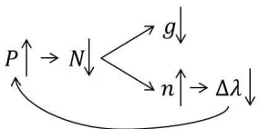
As the input signal starts to increase (at approx. 4 µs) the charge carriers density depletes, at the same time that the refractive index increases. This shifts the longitudinal modes to longer wavelengths, bringing one of them closer to the modulated optical signal wavelength. Between 5µs and the time of the spike in the output signal (at approx. 7 µs) we can see how the output rises continuously. This means that the input optical signal is experiencing optical gain as its wavelength is being reached by the resonant mode, thanks to the nonlinear refractive index increase. As the wavelengths match, more positive optical feedback (constructive interference) builds inside the resonant cavity.
When the longitudinal mode and the input optical signal wavelength are close enough the upward spike in the output signal occurs. The optical signal input power required to reach this condition is called the upward-switching threshold of the bistable hysteresis. After this point, the input signal continues to experience optical gain.
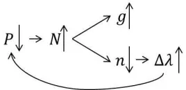
As the input signal starts to drop (around 12 µs), the output signal drops too. The wavelength of the resonant mode shifts back to shorter wavelengths as the carrier density increases and the refractive index decreases. Shifting back makes the input signal experience less optical gain up to a point where the resonance separates sufficiently to produce the downward spike in the output signal (around 18 µs). The optical signal required to reach this point is called the downward-switching threshold
Note that for an input signal voltage of about 1.5 mV we have two possible signal output voltages. In Figure 17 we can see that they do not happen simultaneously. Having one output before the upward-switching threshold and one output after the switching threshold is a dependence on the past state of the bistability.
Figure 18 shows the hysteresis curve of the SOA, obtained when the FP-SOA output power is plotted against its input under a bistable regime of operation. Due to the FP-SOA optical bistability, now a single input power can have two vertically separated output powers, and being in either the “high” or the “low” branch depends if the resonance shift was enough for the resonance to reach the wavelength of the injected signal.
Figure 18. [a] RT-SOA bistable hysteresis – [b] Zoomed in
Upward-switching threshold Downward-switching threshold
a
b
c d
[image:44.595.113.482.414.700.2]The hysteresis plot of Figure 18 is useful to explain the succession of events that lead to the bistability. Let us start with the premise that the refractive index of the resonant cavity is dependent on the power of the light that is travelling within it.
[image:45.595.230.372.556.627.2]The action of feeding the FP-SOA with an optical sine-shaped signal dynamically raises and lowers the refractive index. When the input power is raised (Figure 18 - arrow a), the resonant mode of the amplifier shifts towards longer wavelengths (the refractive index increases) until the wavelength of the resonant mode gets closer to the one of the input optical signal. The input signal power required for this is the upward-switching threshold (Figure 18 - arrow b). When the wavelength detuning between the peak of the longitudinal mode and the input optical signal is sufficiently small, a positive feedback loop (Figure 19) that triggers the high state of the bistable hysteresis occurs. This feedback mechanism is driven by the increasing optical gain that the beam is experiencing at such a short wavelength detuning, and abruptly “pulls” the longitudinal mode close to the wavelength of the input optical signal.
Figure 19. Positive feedback loop that triggers the high bistable state.
optical signal voltage starts to “ride-down”, the output optical signal does the same (Figure 18 - arrow d). Remember that when the input optical signal is lowered, the refractive index decreases, the spectrum moves to shorter wavelengths and the resonance separates from the optical signal wavelength (optical gain drops) [10].
[image:46.595.234.368.507.572.2]The input optical signal at where the resonance shifts to shorter wavelengths enough to separate from the optical signal is called the downward-switching threshold (Figure 18 – arrow d). When the wavelength detuning between the peak of the longitudinal mode and the input optical signal is sufficiently big, a negative feedback loop (Figure 20) that triggers the low state of the bistable hysteresis occurs instead. This mechanism is driven by the decreasing optical gain that the beam is experiencing at such a long wavelength detuning, and abruptly “separates” the longitudinal mode far off the wavelength of the input optical signal. The whole feedback process is then repeated with the arrival of the next sine-shaped optical input pulse.
Figure 20. Negative feedback loop that triggers the low bistable state.
resonances are further apart from the modulated optical signal wavelength, more optical input power is required bring them sufficiently closer to achieve bistability. The increases in the starting optical output power are due to an increase in the optical gain inside the cavity when the FP-SOA injection current is increased.
Figure 21. [a] Hysteresis behavior for different injection currents – [b] Zoomed in
66 mA
65 mA 64 mA
63 mA
[image:47.595.115.476.238.661.2]II.5
Dependence on Input Polarization
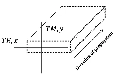
In the introduction it was pointed out that some optical devices like the FP-SOA are polarization sensitive. Technically speaking, this means that their performance depends on the plane of vibration that the electric field components form in a plane transverse (perpendicular) to the direction of propagation.
For this thesis, we are going to set two cases of these planes (perpendicular between each other) as delimiters for our analysis. They are called the transverse
electric (TE) and the transverse magnetic (TM) modes.
If the electric field lays aligned with the x axis of the SOA waveguide, the wave propagates in the transverse electric (TE) mode. On the other hand if the electric field is aligned with the y axis of the SOA waveguide, the wave propagates in
the transverse magnetic (TM) mode. Figure 22 helps in locating where these modes
[image:48.595.194.383.530.659.2]lay with respect to the amplifier axes.
It is known that the effective refractive index for the TE and the TM mode is not equal in SOAs. The difference between both indexes is known as modal
birefringence, determined as [10]:
( ) 2.5
with and being the effective refractive indexes for the TE and TM modes of the waveguide.
From the previous experiments, we observed that the refractive index of the resonant cavity (which contains a waveguide) is modified nonlinearly by the carrier density. Now both effective refractive indexes are going to be modified when an optical signal is coupled into the SOA, similar to [10]:
( ) (
) 2.6
( ) (
)
2.7
If we rotate our input polarization away from either mode, light will couple unevenly between them. As this happens, our electric field components will experience two different refractive indexes that will alter their phase, ultimately producing a change in the polarization of the signal. This is change in polarization is known as polarization rotation.
The confinement factor is another parameter that is not equal for both modes. This factor is defined as the fraction of the mode energy confined to the active layer. In other words, the confinement factor expresses how much of the mode energy will actually experience optical gain, thus, the gain is not going to be equal for both modes. This is shown in Eq. 2.8 and 2.9 below:
( ) (
) 2.8
( ) (
)
2.9
with and being the gain coefficients for each mode.
Being in the TE mode means that the SOP of both bistable states barely varies in time, since the components of the electric field are both experiencing the same refractive index (minimizing the modal birefringence effect). This translates in having a ∆Pol value close to 0 degrees. Figure 23 shows the Poincaré Sphere when the electric field is propagating in the TE mode. Note that the SOP is fixed in one state for this case.
When the input optical signal polarization is rotated away of the TE mode, the components of its electric field will instead experience different refractive indexes. This will affect their phase as they propagate through the SOA, changing their SOP. This SOP evolution is going to be traced out in the Poincaré Sphere, as shown in Figure 24. Remember also that these indexes are also going to be dependent on the carrier density, as shown in Eq. 2.6 and 2.7.
Mathematically, the relations between the Stokes Parameters and the phase difference between the components of the electric field is expressed as:
2.10
2.11
( )
( )
2.12
( )
( )
2.13
( ) ( )
( ) ( )
( )
2.14 2.15 2.16
Figure 25. Spherical coordinates representation of an SOP in the Poincaré Sphere.
Figure 26 shows the effect on the bistable hysteresis when the electric field of the input optical signal is rotated away from the TE mode. The injection current was fixed at 67 mA.
𝑠
𝑠 𝑠
𝛹
Figure 26. Hysteresis behavior for different input polarizations.
input polarization) raises the upward-switching threshold and lowers the optical gain. The difference in the optical gain experienced by the signals as its SOP changes progressively can be attributed also to the fact that the TE mode has a higher confinement factor than the TM mode [11], which agrees with the results shown in Figure 26. Figure 27 shows all the cases superposed, so the hysteresis upward-switching thresholds shift and the reduction in optical gain is better appreciated.
Figure 27. [a] Hysteresis behavior for different input polarizations – [b] Zoomed in.
Figure 28 shows that as the input optical signal polarization is rotated ∆Pol rises. This means that when the input optical signal is misaligned from the TE mode it is experiencing two different refractive indexes. Not only this, also the carrier density
51.57° 40.84°
23.26° 0.91°
[image:56.595.110.494.305.614.2]is changing because the varying input signal power is inducing carrier depletion and recovery constantly, also modifying both refractive indexes. All of this affects the phase of the components of the electric field of the signal, ultimately changing its SOP through nonlinear polarization rotation (NPR).
Figure 28. Evolution of ∆Pol with the polarization rotation of the optical input signal.
switching threshold by the average optical signal power output of the FP-SOA before the upward-switching threshold.
[image:58.595.137.472.355.612.2]Figure 29 shows the hysteresis contrast and the upward-switching threshold power requirement and their dependence on the optical input polarization. It shows that propagating in the TE mode yields the best hysteresis contrast and has the lowest upward-switching threshold power requirement, while propagating in any other mode yields worst contrasts and higher optical power requirement to reach the upward-switching threshold.
Figure 29. Evolution of the hysteresis contrast and the upward-switching threshold as ∆Pol increases.
Hysteresis
III.
AOFF Contrast Enhancement via its
Input Polarization
In this chapter, an RT-SOA-based AOFF similar to the one demonstrated by Maywar, et al. [6] is going to be introduced. In this setup however, a hybrid control of the AOFF is going to be the responsible for its flip-flop operation. After experimenting with this hybrid control, the polarization dependence of the AOFF to changes in its input polarization will be analyzed. The experiments performed in this chapter clearly show how to optimize the on-off switching contrast to around 8 dB, where all previously published contrasts were around 3 dB.
III.1
Hybrid Control of an AOFF
The approach used by Maywar, et al. [6] in their RT-SOA flip-flop setup was to have continuous-wave (CW) “holding” beam (HB) passing through an auxiliary TW-SOA whose output power is modulated by two control signals inducing XGM. This modulation will make the power of the HB fall above and below the bistable hysteresis switching thresholds of the RT-SOA, achieving flip-flop operation. In this approach, the reset signal falls within the gain profile of the TW-SOA and can have quite low power.
RT-SOA and move its resonances by XPM. In this approach, the set signal falls within the gain profile of the RT-SOA and can therefore have quite low power.
A hybrid control approach has the reset control pulse modulating remotely via
XGM the power of a HB passing through an auxiliary TW-SOA, but now the set control pulse is inducing XPM directly in the RT-SOA as shown in Figure 30. The modulated output power of the TW-SOA and the set control pulse inducing XPM of the RT-SOA will both affect the refractive index of the device, shifting the longitudinal modes to the short and the long side of the spectrum, unlatching and
latching the HB. The latching mechanism depends once again on the power of the HB
[image:60.595.101.493.398.697.2]falling above and below the switching thresholds of the bistable hysteresis.
A 1580-nm 8-dBm CW beam from a Santec TSL-210V tunable laser gets modulated into 62.5 KHz optical set pulses by an EOSpace MZM (model PM-0K5-10-PFA-PFA). The MZM is RF driven by a Picosecond Pulse Labs 12010 pulse pattern generator. Figure 31 shows a screen capture of the oscilloscope of the set pulses.
The 1557-nm 9-dBm beam from a NEC NX8563LA DFB laser diode controlled by an ILX Lightwave LDC-3900 module gets modulated into 62.5 KHz
reset pulses by an EOSpace Mach-Zehnder (same model) amplitude modulator, RF
[image:61.595.129.467.444.707.2]driven by the second channel of the pattern generator used for the set pulse. The set and the reset control pulses are separated by 60 µs between each other. The reset pulses have the same shape as those in Figure 31.
Optical circulators are 3-port devices placed at the points shown in Figure 30 to separate the signals that travel in opposite directions. The also allow bi-directional transmission on a single fiber. For example, the circulator that is between the HB laser and the TW-SOA allows the HB to go into the SOA, but the TW-SOA reflected signal exits through the 3rd port of the circulator, and they do not reflect back through the input fiber. Because of their high isolation between the input and reflected optical powers; they are perfect for cancelling unwanted reflections back to the SOAs or MZMs.
The 1599-nm 0-dBm HB comes from a Santec TSL-510V tunable laser. The TW-SOA is a CIP model SOA-XN-OEC-1550 SOA controlled by an ILX Lightwave LDC-3908 module providing an injection current of 54.3mA at 20°. Finally the FP-SOA is a CIP model FP-SOA-NL-OEC-1550-A17 FP-SOA, controlled also by the LDC-3908 providing an injection current of 67 mA at 20°.
For the diagnostics, right at the exit of the FP-SOA lays a General Photonics POD-101D polarimeter to monitor the polarization of the bistable states of the AOFF as shown in Figure 32.
The optical amplifier is an L-band EDFA from Amonics (model AEDFA-L-PA-25-FA) with both pumps at 200mA (as it yielded the flattest ASE spectrum for our wavelengths). The EDFA boosts the power of the flip-flop signal for measurement by the photodiodes. An optical tunable filter from Alnair Labs (model BVF-200CL) is used to suppress the ASE spectrum of the EDFA.
We will now discuss the hybrid-controlled AOFF with the help of Figure 33 and Figure 34:
Figure 33. The hybrid control approach. [a] is the set pulse riding along the HB CW power and the XGM induced HB voltage drop by action of the reset pulse – [b] shows the FP-SOA transmitted power output in
AOFF operation – [c] shows the FP-SOA reflected power output in AOFF operation
SET state
RESET state RESET state SET state
SET
RESET
SET SET
The moment the set pulse enters directly into the FP-SOA, it induces a carrier depletion that increases the refractive index of the FP-SOA, shifting the spectrum to longer wavelengths via XPM. This XPM shifting is analogous to the one occurring in Figure 15 of the previous chapter. When the spectrum shifts it latches the wavelength of the HB, making it coincide with the resonance peak of the previously slightly-detuned longitudinal mode. When this happens, there is a sudden increase in optical power due to constructive interference. This increase in optical input power achieves the upper-switching threshold of the bistable hysteresis, making the flip-flop reach its “on” state.
Figure 34. FP-SOA spectrum for each bistable state of the AOFF.
Now, when the reset pulse arrives to the TW-SOA, the HB power drops. This XGM-generated drop raises the carrier density inside the FP-SOA, decreasing its refractive index via XPM, and shifting its spectrum to shorter wavelengths. Increasing the carrier density raises the optical power of the longitudinal modes, as shown in Figure 34.
As it is shifted, the HB experiences less optical gain as it is being separated from the peak resonance wavelength and at some point; its power drops enough to reach the lower-switching threshold of the bistable hysteresis. When this happens, the AOFF switches to its lower power, “off” state as shown in Figure 34. The process is then repeated, giving the output its characteristic square-wave shape. Under these
1599 1599.1 1599.2 1599.3 1599.4 1599.5 1599.6 1599.7 1599.8 1599.9 1600 -70 -60 -50 -40 -30 -20 -10 F P -S O A S p e c tr u m [ d B m ] Wavelength [nm] AOFF on the SET state
experimental conditions, the AOFF exhibited a switching contrast of around 3 dB, as shown in Figure 33 and Figure 34.
III.2
Impact of Input Polarization
As it was shown in Figure 29, aligning the input SOP to the TE mode of the FP-SOA appears to yield the best bistable hysteresis in terms of having a maximum contrast and a lowest upward-switching threshold power requirement. To see if such observation could raise the 3 dB switching contrast of the AOFF shown in the previous section, the input HB will be rotated from a random starting input SOP until the AOFF output shows a ∆Pol of 0 degrees. When this condition is reached, the input HB will be propagating in the TE mode of the FP-SOA, and we can compare if the switching contrast is the best amongst different input SOPs.
To try different input SOPs of the HB and reach the case where it propagates in the TE mode of the SOA, we must adjust the polarization controller right before the FP-SOA and tweak the HB optical power. All this while paying attention to the Poincaré Sphere and the ∆Pol parameter described in it by the bistable states. The HB power adjustment is needed as different SOP inputs (especially those that are not aligned with the TE mode of the SOA) have higher upward-switching thresholds. (Figure 29).
Figure 35. AOFF output powers to different HB input polarizations.
Figure 36. [a] AOFF output powers – [b] Switching temporal & spectral contrast for different HB input polarizations.
41.89°
18.97° 4.36° 0.72° 44.53°
37.65° 46.47°
∆𝐏𝐨𝐥
OFF state
As in the previous observations, different HB input SOPs couple the HB optical power unevenly between the TE and TM propagation modes of the SOA. This affects the phase difference between the components of the HB electric field and also how much optical gain each state experiences. This can be attributed to the different confinement factor of the TE and TM modes. The on state is less affected by the rotation, but the off state voltage level rises constantly as the HB polarization rotates away of TE, increasing ∆Pol.
Figure 37 shows that the dependence of the bistable outputs of the AOFF to its input beam SOP matches the dependence of the bistable hysteresis characterization done in section II.5. As it was expected, the AOFF is just two “discrete” output powers of each branch of the bistable hysteresis of the FP-SOA. Having an input SOP that makes the beam propagate in the TE mode of the SOA yields once again the best temporal switching contrast. This best case also has the lowest upward-switching power requirement, which agrees with the results of section II.5.
Figure 36 [b] also shows that both the temporal and spectral contrast agree with each other. This is a reassuring result as in photonics; the temporal and spectral contrast should be the same. The relationship between power and voltage in the optical world
is , with being the responsivity of the photodiode. This means that
calculating the switching contrast in the oscilloscope with voltage readings or in the OSA with power readings yields the same result, as the ratio of the terms cancels the
( )
3.1
(
) 3.2
with
[ ] [ ]
[ ]
[image:70.595.181.501.78.390.2]
[ ]
Figure 37. Switching contrast vs. rotation and power increase of the HB.
[image:71.595.143.469.102.357.2]We suspect that ignoring the polarization dependence of the AOFF was the reason for achieving the previously reported contrasts of around 3 dB. Using the optimization process shown before, we achieved a temporal and spectral switching contrast of around 8.2 dB, advancing the state-of-the-art for AOFF based in RT-SOA. The switching contrasts for all the rotations are shown in Table 1.
Table 1. Switching contrast for all the rotations.
∆Pol [degrees]
Temporal switching contrast [dB]
Spectral switching contrast [dB]
0.79 8.24 8.25
4.36 6.62 6.89
18.98 4.94 6.36
37.66 3.99 3.779
41.89 3.37 3.1
44.53 2.90 2.58
46.47 2.46 2.2
Switching contrast
IV.
AOFF Contrast Enhancement via its
Output Polarization
Chapter III showed that the HB input SOP is crucial in obtaining the best switching contrast of the AOFF. The best switching contrast of around 8.2 dB of the previous chapter coincided with having the HB input SOP aligned to the TE mode of the FP-SOA; any other case yielded worse results. Another observation was that as the HB input polarization is rotated away from the TE mode, the bistable output states exhibit different SOPs. The more misaligned the HB is, the more dissimilar these SOPs are, as shown in Figure 37.
Figure 38. The difference in SOP of both bistable states seen in the Poincaré Sphere.
In this chapter, the SOP of the low (off) bistable output of the AOFF is rotated with a polarization controller until it is perpendicular to the transmitting plane of an in-line polarizer. When this condition is met, the polarizer suppresses the low output of the AOFF by absorption. The increase in switching contrast due to the polarizer is directly linked to how dissimilar the SOPs of the bistable states are.
With this technique, we measured a temporal switching contrast of 13.89 dB, while spectrally; the switching contrast was over 35 dB. The explanation for such difference can be found at the end of this chapter.
SET state
The experimental setup is similar to that in the previous chapter; the only difference is the addition of a polarization controller and a General Photonics in-line polarizer with an extinction ratio of 32 dB. Both are located after the polarimeter, as shown in Figure 39. The HB controller was set at -2 dBm output power.
IV.1
Demonstration of Contrast Enhancement
[image:75.595.116.477.267.561.2]Figure 40 shows the output of the FP-SOA in AOFF operation before introducing the polarizer. The switching contrast in this case is 2.833 dB and the ∆Pol of the AOFF bistable states was 41.36°. The average power value for the high output state was 15.28 mV, while the average power output of the low state was 7.978 mV.
Figure 40. Output of the FP-SOA in AOFF operation before introducing the polarizer.
ON state
Then the polarizer was introduced. The procedure used to align the SOP of the low AOFF bistable output so it is perpendicular to the transmitting plane of the polarizer is as follows:
1. With the FP-SOA in AOFF mode, the set optical control pulse is removed and then the reset pulse is removed. By doing this, the AOFF is fixed in its “off” state and the SOP corresponds to it.
2. Now, with the help of the OSA as a power monitor, the SOP of the “off” state is rotated until it achieves maximum suppression. The technique for doing this is placing the OSA marker on top of the HB wavelength, setting the OSA in the “repeat sweep” mode with a sweep span of 0 nm, selecting a high sensitivity mode, and selecting the smallest wavelength resolution possible (0.02 nm for our OSA). This way the OSA will show the peak power of the HB at only one wavelength. This configuration turns the OSA into a sensitive sweeping power monitor to immediately see the changes of the HB power coming out of the polarizer as its SOP is rotated.
Figure 41 shows the output of the FP-SOA in AOFF after introducing the polarizer and performing the alignment procedure:
Figure 41. Output of the FP-SOA in AOFF operation after introducing the polarizer.
The switching contrast in these conditions rose to 13.89 dB. Note that using the polarizer and blocking the SOP of the low output state of the AOFF dropped its power to an average of 396 µV, while the high output power average dropped to 8.77 mV.
polarization of the HB is rotated further than in the cases of Figure 27 in the quest of a larger ∆Pol, the dispersive bistability of the AOFF is no longer achievable because the bistable hysteresis upward-switching threshold moves to larger values of power that are not attainable by our input signal.
Figure 42. AOFF spectrum fixed in the SET state before and after placing the polarizer.
1599.3 1599.4 1599.5 1599.6 1599.7 1599.8 1599.9 1600 1600.1 -80 -70 -60 -50 -40 -30 -20 -10 0 F P -S O A S p e c tr u m [ d B m ] Wavelength [nm]
AFTER the polarizer -24.87 dB
BEFORE the polarizer -16.89 dB
1599.3 1599.4 1599.5 1599.6 1599.7 1599.8 1599.9 1600 1600.1 -80 -70 -60 -50 -40 -30 -20 -10 0 F P -S O A S p e c tr u m [ d B m ] Wavelength [nm]
BEFORE the polarizer -19.4 dB
[image:79.595.116.483.434.728.2]In Figure 42 we can appreciate a spectral contrast drop of -7.98 of the set state of the AOFF before and after placing the polarizer. Temporally, this corresponds to the temporal power drop of the high output experienced by the AOFF signal between Figure 40 and Figure 41. In Figure 43 we can see a dramatic spectral suppression of the low output state power after introducing the polarizer. Carefully aligning its SOP so it corresponds to the blocking state of the polarizer causes a drop of 42.12 dB in power.
[image:80.595.111.480.402.693.2]Figure 44 shows the HB power of both bistable cases after the polarizer was introduced. In this figure, the difference in the switching spectral contrasts can be better appreciated.
Figure 44. FP-SOA spectrum of both bistable outputs after placing the polarizer.
1599.3 1599.4 1599.5 1599.6 1599.7 1599.8 1599.9 1600 1600.1 -80 -70 -60 -50 -40 -30 -20 -10 0 F P -S O A S p e c tr u m [ d B m ] Wavelength [nm] SET state -24.87 dB
V.
Concluding Remarks
This thesis explored the polarization dependence of RT-SOAs and how this can be used to significantly optimize the switching contrast between the bistable states of a novel, hybrid-controlled RT-SOA-based AOFF. This significant boost in the switching contrast makes this type of AOFF an attractive choice for future all-optical sequential signal processing devices.
We first experimentally characterized the dispersive bistability of RT-SOAs and the intricacies between its key parameters, such as the carrier density and injection current, with the refractive index and gain of the amplifier. Then we built on the knowledge acquired by rotating the input HB SOP and characterizing once again how the dispersive bistability behaved. We showed that propagating in the TE mode yields the best hysteresis contrast and has the lowest upward-switching threshold power, while propagating in any other mode yields worse contrasts and higher optical power to reach the upward-switching threshold.
suspect that ignoring the polarization dependence of the AOFF was the reason for achieving the previously reported contrasts of around 3 dB.
Given that not having an aligned HB SOP input into the FP-SOA yielded broader SOP rotation between both bistable outputs of the AOFF, we moved on to explore the possibility of “blocking” one of these outputs using a polarizer. We demonstrated that by using this polarization blocking technique we achieved an on/off switching contrast of 36.6 dB with an optical signal-to-noise ratio (OSNR) of 34.42 dB, setting an absolute new benchmark for switching contrasts of RT-SOA-based AOFFs.
Summarizing our contributions:
Experimentally showed dependence on polarization of the dispersive bistability of RT-SOAs.
Demonstrated a novel, hybrid-controlled RT-SOA-based AOFF and its polarization dependence. With this knowledge, we demonstrated an optimization technique that yielded a switching contrast of 8.2 dB, advancing the state-of-the-art for AOFF based in RT-SOAs.
VI.
Appendix: Tips on using the Polarimeter
In this chapter, we offer a few tips when using the General Photonics POD-101D polarimeter.
First of all, note that the maximum sampling rate of the POD-101D is 625 kS/s, which is relatively low. In order to comply with the Nyquist sampling theorem, the frequency of the signal to analyze must not exceed 62.5 KHz. If the signal is faster 62.5 KHz, the SOP displayed will not accurately represent its true value.
When using an external trigger source, be mindful that the voltage level arriving to the polarimeter is sufficient to actually trigger the device. This is critical especially when sharing the same trigger source amongst multiple
![Figure 18. [a] RT-SOA bistable hysteresis – [b] Zoomed in](https://thumb-us.123doks.com/thumbv2/123dok_us/48150.4393/44.595.113.482.414.700/figure-a-rt-soa-bistable-hysteresis-zoomed-in.webp)
![Figure 21. [a] Hysteresis behavior for different injection currents – [b] Zoomed in](https://thumb-us.123doks.com/thumbv2/123dok_us/48150.4393/47.595.115.476.238.661/figure-hysteresis-behavior-different-injection-currents-b-zoomed.webp)