Rochester Institute of Technology
RIT Scholar Works
Theses
Thesis/Dissertation Collections
3-1-2011
Towards integrating chalcogenide based phase
change memory with silicon microelectronics
Archana Devasia
Follow this and additional works at:
http://scholarworks.rit.edu/theses
This Dissertation is brought to you for free and open access by the Thesis/Dissertation Collections at RIT Scholar Works. It has been accepted for inclusion in Theses by an authorized administrator of RIT Scholar Works. For more information, please [email protected].
Recommended Citation
TOWARDS INTEGRATING CHALCOGENIDE BASED
PHASE CHANGE MEMORY WITH SILICON
MICROELECTRONICS
by
ARCHANA DEVASIA
A DISSERTATION
Submitted in partial fulfillment of the requirements
For the degree of Doctor of Philosophy
in
Microsystems Engineering
at the
Rochester Institute of Technology
March 2011
Author: ____________________________________________________________________
Microsystems Engineering Program
Certified by: ________________________________________________________________
Santosh K. Kurinec, Ph.D.
Professor of Electrical and Microelectronic Engineering
Approved by: _______________________________________________________________
Bruce W. Smith, Ph.D.
Director of Microsystems Engineering Program
ii
NOTICE OF COPYRIGHT
© 2011
Archana Devasia
REPRODUCTION PERMISSION STATEMENT
Permission Granted
TITLE:
“Towards Integrating Chalcogenide based Phase Change Memory with Silicon
Microelectronics”
I,
Archana Devasia
, hereby grant permission to the Wallace Library of the Rochester
Institute of Technology to reproduce my dissertation in whole or in part. Any reproduction
will not be for commercial use or profit.
iii
Towards Integrating Chalcogenide based Phase Change Memory
with Silicon Microelectronics
By
Archana Devasia
Submitted by Archana Devasia in partial fulfillment of the requirements for the degree of Doctor of Philosophy in Microsystems Engineering and accepted on behalf of the Rochester Institute of Technology by the dissertation committee.
We, the undersigned members of the Faculty of the Rochester Institute of Technology, certify that we have advised and/or supervised the candidate on the work described in this dissertation. We further certify that we have reviewed the dissertation manuscript and approve it in partial fulfillment of the requirements of the degree of Doctor of Philosophy in Microsystems Engineering.
Approved by:
Dr. Santosh K. Kurinec
(Committee Chair and Dissertation Advisor)
Dr. Robert E. Pearson
Dr. Surendra K. Gupta
Dr. Karl D. Hirschman
Dr. Kristy A. Campbell
Dr. Bruce W. Smith
(Director, Microsystems Engineering)
Dr. Harvey J. Palmer
(Dean, Kate Gleason College of Engineering)
iv ABSTRACT
Kate Gleason College of Engineering Rochester Institute of Technology
Degree Doctor of Philosophy Program Microsystems Engineering Name of Candidate Archana Devasia
Title Towards Integrating Chalcogenide based Phase Change Memory with Silicon Microelectronics
The continued dominance of floating gate technology as the premier non-volatile memory (NVM) technology is expected to hit a roadblock due to issues associated with its inability to catch up with CMOS scaling. The uncertain future of floating gate memory has led to a host of unorthodox NVM technologies to surface as potential heirs. Among the mix is phase change memory (PCM), which is a non-volatile, resistance variable, memory technology wherein the state of the memory bit is defined by the resistance of the memory material. This research study examines novel, bilayer chalcogenide based materials composed of Ge-chalcogenide (GeTe or Ge2Se3) and Sn-chalcogenide
(SnTe or SnSe) for phase change memory applications and explores their integration with CMOS technology. By using a layered arrangement, it is possible to induce phase change response in materials, which normally do not exhibit such behavior, and thus form new materials which may have lower threshold voltage and programming current requirements. Also, through the incorporation of a metal containing layer, the phase transition characteristics of the memory layer can be tailored in order to obtain in-situ, a material with optimized phase change properties. Using X-ray diffraction (XRD) and time resolved XRD, it has been demonstrated that stacked phase change memory films exhibit both structural and compositional dependency with annealing temperature. The outcome of the structural transformation of the bottom layer, is an annealing temperature dependent residual stress. By the incorporation of a Sn layer, the phase transition characteristics of Ge-chalcogenide thin films can be tuned. Clear evidence of thermally induced Ge, Sn and chalcogen inter-diffusion, has been discerned via transmission electron microscopy and parallel electron energy loss spectroscopy. The presence of Al2O3 as capping layer has been found to mitigate volatilization and metallic Sn
phase separation at high temperatures. Two terminal PCM cells employing these bilayers have been designed, fabricated and tested. All devices exhibit threshold switching and memory switching behavior. By the application of suitable voltage programming pulses, RESET state switching can be accomplished in these devices, thus demonstrating single bit memory functionality. A process for integrating bilayer PCM technology with 2 µm CMOS has been designed and developed. The baseline RIT CMOS process has been modified to incorporate 12 levels of photolithography, 3 levels of metal and the addition of PCM as a BEOL process. On electrical testing, NMOS connected PCM devices exhibit switching behavior. The effect of the state (SET/RESET) of the series connected PCM cell on the drain current of the NMOS has also been investigated. It is determined that threshold switching of the PCM cell is essential in order to observe any change in MOS drain current with variation in drain voltage. Thus, successful integration of bilayer PCM with CMOS has been demonstrated.
v
vi
I solemnly swear that I am up to no good….
- J. K. Rowling
vii
Acknowledgements
My advisor Dr. Santosh Kurinec has been to me what Albus Dumbledore has been to Harry Potter. To Potter enthusiasts this statement says it all, however for the sake of those ‘muggles’ who have been able to resist the charm of the boy with the lightening scar, I feel compelled to elaborate. I am exceedingly grateful to her for giving me a platform that I could use to learn to conduct independent research. She played a cardinal role in broadening my scientific outlook by providing me with multiple opportunities to collaborate with research groups and scientists around the country. Her vibrant demeanor and highly individual viewpoint helped me fashion my own attitude towards science. She has been variously a mentor, a friend, a teacher and at times even a parent. I owe her all my success.
viii
Many thanks go to Dr. Bruce Smith who helped me keep my progress on track and my eye on the final prize. I would like to specially acknowledge Dr. Lynn Fuller, my very own personal Superman. Both inside and outside the cleanroom, his expertise always steered me in the right direction. My thanks to Dr. Simone Raoux from IBM for providing me with the opportunity of a lifetime by giving me a chance to work with her at the National Synchrotron Light Source at Brookhaven National Laboratory. She has been wonderful in critiquing my ideas, providing me with steadfast guidance and encouragement and looking out for me during my internship at IBM. I am also grateful to Dr. Feiming Bai for support with XRD measurements and data interpretation. He was instrumental in helping me gain a practical understanding of the field. My deepest thanks go to the amazing duo of Morgan Davis and Jennifer Regner from Boise State University who helped me out with all my chalcogenide depositions and ion milling runs. I would also like to express my sincere gratitude to David MacMahon from Micron for carrying out TEM and PEELS measurements on several of my samples.
ix
PE4400 just so that my work would not suffer. Generations of cheeky students have been transformed into ‘tool manual abiding’, responsible users by the acerbic tongue of Rich Battaglia and I am not an exception. With his sarcastic sense of humor, he always kept me on my toes. Thanks to David Yackoff for maintaining the Canon in excellent condition. To this day it has been one of the most rewarding tools to work with. Special thanks go to Tom Grimsley for writing numerous masks, trusting me with off-hours fab access, repeatedly admonishing me for not wearing my safety glasses in those early years when I was a cheeky student, volunteering to be my off-hours buddy on a Sunday when no one was available and basically doing everything possible so that I could get my processing done. I am also indebted to the ever so approachable Scott Blondel who was always available lest the need arise.
x
I would like to express my gratitude to the incredible Sharon Stevens for administrative support and also to the phenomenal Sara Widlund for sending and receiving FedEx packages for me from all over the country.
Special thanks go to Karthik Narayanan my wonderful roommate for 4 years. Our shared love of movies, Indian food, a certain wizard, the girl with the dragon tattoo and a certain Food Management class offered at RIT, made the time spent in Rochester one of the most glorious times of my life.
My heartfelt thanks go to my partner in crime Prudhvi Gurram. We began this journey together at RIT and have now become partners in life. He not only had the patience to painstakingly go over several revisions of my dissertation but also had the capacity to endure all my thesis related complaints, reproaches, sulks and at times copious amounts of tears. I am genuinely amazed that he asked me to be his wife. I love you Prudhvi and I am truly grateful to have you in my life.
I am blessed to have parents who have always been tremendously supportive of my choices. Though at times they may have been baffled by my decisions – one such time being when I informed them of my resolve to develop a 12 lithography level process at the SMFL - their patience, love and encouragement has been unrelenting. They are the inspiration behind my work and it is only fitting that I dedicate this dissertation to them. I love you both Mama and Papa. You have given me everything that I could have hoped for and more.
And finally, thanks to the extraordinary JKR for giving me the enduring HJP, HJG and RBW.
xi
Table of Contents
List of Figures... xv
List of Tables ... xix
List of Abbreviations ... xx
1 INTRODUCTION ... 1
1.1 Floating Gate Technology... 3
1.1.1 Physical Cell-Scaling Challenges ... 5
1.1.2 Electrical Cell-Scaling Challenges ... 6
1.1.3 Reliability Scaling Challenges... 6
1.2 Non-Conventional Memory Technologies... 7
1.3 Phase Change Memory ... 10
1.4 Scope and Novelty of this Study... 11
2 BACKGROUND OF PHASE CHANGE MEMORY ... 17
2.1 Introduction ... 17
2.2 PCM Device Operation ... 17
2.3 Physical Principles Underlying PCM... 20
2.3.1 Amorphous-Crystalline Phase Transition... 20
2.3.2 Band Structure for Chalcogenide Semiconductors... 21
2.3.3 Conduction in the Crystalline Phase... 22
2.3.4 Conduction in the Amorphous Phase... 24
2.3.5 Mechanism of Threshold Switching ... 29
2.4 Materials Used for Phase Change Memory ... 34
2.4.1 The Pseudo-Binary GeTe-Sb2Te3 Compositions – Class I ... 36
2.4.2 The Compositions Around the Eutectic Point Sb69Te31 – Class II ... 36
2.4.3 Doped GST ... 37
2.4.4 Other Materials ... 37
2.5 Characteristics of GST based PCM cells vis–à-vis requirements of next generation NVM ... 38
2.5.1 Read/Write Times ... 38
2.5.2 Data Retention ... 39
2.5.3 Endurance ... 39
2.5.4 Scalability ... 40
xii
2.5.4.2 Scaling of dissipated power and IRESET... 40
2.5.4.3 Scaling of Voltage ... 41
2.5.4.4 Scaling of Cell Size ... 41
2.5.4.5 Physical Limits of Scaling... 42
2.5.5 Low Power... 42
2.5.5.1 Reducing the Electrode Contact Area ... 43
2.5.5.2 Reducing the Phase Change Material Volume... 44
2.5.5.3 Reducing Both the Material and the Contact ... 45
2.6 Need for Material Engineering... 46
3 MOTIVATION AND RESEARCH OBJECTIVES ... 52
3.1 Motivation ... 52
3.1.1 Choice of Memory Material ... 52
3.1.2 Merits of Using a Tin-Chalcogenide Layer ... 53
3.2 Research Objectives ... 54
4 MATERIAL CHARACTERIZATION ... 57
4.1 Introduction to X-ray Diffraction... 57
4.2 Amorphous-Crystalline Spectrum of Chalcogenides under Investigation... 58
4.3 Residual Stress Analysis ... 59
4.3.1 Sample Preparation ... 59
4.3.2 Stress Measurement Technique ... 60
4.3.3 Extraction of 1D profile from 2D data... 62
4.3.4 Results and Discussion ... 63
4.3.4.1 Ge2Se3/SnTe Stack ... 63
4.3.3.2 GeTe/SnTe Stack... 67
4.4 Examination of Phase Transition using Time-resolved XRD... 69
4.4.1 Time-resolved XRD using Synchrotron Radiation... 69
4.4.2 Sample Preparation ... 71
4.4.3 Experiment... 71
4.4.4 Results and Discussion ... 71
4.4.3.1 GeTe/SnSe... 72
4.4.3.2 Ge2Se3/SnTe ... 74
4.5 Investigation of Material Inter-diffusion via Time-resolved XRD, TEM and PEELS ... 76
4.5.1 Overview of PEELS Technique... 76
xiii
4.5.3 Experiment... 78
4.5.4 Results and Discussion ... 79
4.6 Summary of Results ... 84
4.7 Resistivity v/s Temperature Measurements of Single Layers... 85
4.7.1 GeTe... 85
4.7.2 SnSe ... 86
4.7.3 SnTe ... 86
4.8 Conclusions ... 86
5 TWO TERMINAL PHASE CHANGE MEMORY DEVICES ... 91
5.1 Concept ... 91
5.2 Mask Layout... 92
5.3 Fabrication... 93
5.3.1 Substrate Preparation ... 94
5.3.2 Bottom Electrode Formation ... 94
5.3.3 Inter-level Dielectric Deposition ... 95
5.3.4 Sputter clean ... 95
5.3.5 Chalcogenide Evaporation... 96
5.3.6 Top Electrode Formation ... 97
5.4 Electrical Testing ... 97
5.4.1 Determination of I-V Characteristics ... 98
5.4.2 Programming the PCM Devices ... 100
5.5 Conclusions ... 103
6: INTEGRATION OF BILAYER PCM CELLS WITH CMOS ... 105
6.1 Introduction ... 105
6.2 Concept ... 105
6.3 Design and Mask Layout ... 108
6.3.1 Read Circuitry... 108
6.3.1.1 Sense Amplifier ... 110
6.3.1.2 Adjustable Current Source ... 112
6.3.1.3 Tri-state Buffer ... 114
6.3.1.4 Comparator ... 114
6.3.2 Write Circuitry... 114
6.3.2.1 Write Drive Circuit... 115
xiv
6.3.4 Bit Line Decoder... 117
6.4 Fabrication... 118
6.4.1 Substrate Acquisition and Preparation... 118
6.4.2 N-well Formation... 119
6.4.3 P-well Formation ... 119
6.4.4 Twin Well Drive In... 120
6.4.5 Active Area Definition... 120
6.4.5 Channel Stop Implant ... 121
6.4.6 Field Oxide Growth ... 121
6.4.7 Kooi Oxide Growth ... 121
6.4.8 Threshold Voltage Adjust Implant ... 122
6.4.9 Gate Oxide Growth... 122
6.4.10 Gate Formation ... 123
6.4.11 N+ Source/Drain Formation ... 123
6.4.12 P+ Source/Drain Formation... 124
6.4.13 Polysilicon Re-oxidation... 124
6.4.14 Pre-metal Dielectric Deposition... 124
6.4.15 Source/Drain Anneal... 124
6.4.16 Contact Cut Formation... 125
6.4.17 Metal 1 Deposition... 125
6.4.18 ILD 1 Deposition and Via 1 Formation ... 126
6.4.19 Metal 2 Deposition... 126
6.4.20 ILD 2 Deposition and Via 2 Formation ... 127
6.4.21 Sputter Clean and Chalcogenide Evaporation ... 127
6.4.22 Metal 3 Deposition... 128
6.5 Electrical Testing of MOS Integrated PCM Devices... 128
6.5.1 DC Current Sweep ... 129
6.5.2 MOSFET Output Characteristics... 131
6.6 Conclusions ... 132
7 SUMMARY AND CONCLUSIONS... 134
APPENDIX A: MOSFET Parameter Extraction... 141
xv
List of Figures
1.1 Quantity trend of EEPROM, NOR Flash, NAND Flash and electronic system ... 1
1.2 NVM penetration rate in electronic systems ... 2
1.3 Quantity trend of storage application units ... 3
1.4 (a) Cost-flexibility plane comparison of NVM technologies, (b) NOR+NAND Flash revenue... 3
1.5 (a) Cross section of a typical Flash memory cell, (b) SEM cross section of 65 nm NOR Flash cell ... 4
1.6 Schematic cross-sections and circuit diagrams for NOR and NAND flash memory... 4
2.1 (a) Typical phase change memory cell employing GST, (b)Schematic temperature-time
relationship during programming in a PCM cell ... 18
2.2 I-V characteristics of a PCM cell... 19
2.3 Schematic of volume-temperature variation of a PCM material showing different possible phase transitions ... 21
2.4 Schematic band diagrams and density of states as a function of energy of chalcogenide
material for (a) amorphous phase, (b) crystalline phase... 22
2.5 Schematic of two different mixed-phase configurations, characterized by an incomplete
(State A) or complete (State B) percolation path through low-resistivity grains ... 23
2.6 Measured I-V characteristics for amorphous GST at temperature T = 25, 45, 65 and 85˚C ... 24
2.7 Schematic for sub-threshold conduction via localized states. (a) Electrons trapped at donor- type traps confined by potential Δφ(0) at zero bias, (b) drop in potential barrier to Δφ(V) with application of voltage, V > 0. (c) Profile of electron potential energy along minimum path between localized sates S1 and S2, with electric field F = 0 (top) and F = 0.5 MV cm-1
(bottom) ... 25 2.8 Activation energy as a function of voltage, obtained from experimental I-V curves at variable temperature and from calculations using Eq. (2.12)... 29
2.9 Schematic for (a) energy distribution of electrons in amorphous chalcogenide at equilibrium (no applied electric field), (b) energy distribution of electrons in amorphous chalcogenide under off-equilibrium conditions at high electric field, (c) energy balance in a thin slice dz along the direction of the current in the amorphous region... 31 2.10 (a) Measured I-V curve for a PCM cell with amorphous GST and calculation results obtained from the coupled solution of eqs. (2.10) and (2.22) for different values of amorphous
xvi
explain physical origin of NDR. Calculated profiles for three bias points P1, P2 and P3 for (a) conduction band mobility edge Eʹ′C (solid line) and quasi-Fermi level EF, (b) average
excess energy EF - EF0 ... 33
2.11 Typical compositions of phase change materials ... 36
2.12 Scaling trends of NOR and NAND Flash and PCM technologies ... 41
2.13 Cell engineering, (a) ‘µ’ trench PCM cell, (b) Fabrication of a ‘pore’ PCM cell ... 43
2.13 Cell engineering, (c) TEM of a phase change bridge, (d) Cross sectional view of cross-spacer structure ... 45
3.1 Bilayer chalcogenide based PCM structure... 52
4.1 Diffraction of X-rays by a crystal using Bragg’s law... 57
4.2 2D diffraction frames showing (420) and (422) Debye rings in (a) as-deposited Ge2Se3/SnTe sample and (b) Ge2Se3/SnTe sample annealed to 450 ˚C ... 62
4.3 Diffraction profiles of Ge2Se3/SnTe samples annealed at various temperatures (temperature increases from bottom to top), (b) Annealing temperature dependence of in-plane residual stress, (c) Level view of SnTe (200) peak upon heating. The arrow at ~250 ˚C corresponds to separation of SnSe phase. The arrow at ~350 ˚C represents possible crystallization of Ge2Se3, (d) Variation of d200 with temperature... 64
4.4 (a) Diffraction profiles of GeTe/SnTe samples annealed at various temperatures, (b) Annealing temperature dependence of in-plane residual stress, (c) Variation of d200 with temperature ... 68
4.5 Block diagram of beamline X20C at NSLS ... 70
4.6 XRD profile of as-deposited GeTe/SnSe ... 72
4.7 Peak intensity variation with temperature when sample is heated to, (a) 230 ˚C, and detector centered at 2θ= 37˚, (b) 270 ˚C, and detector centered at 2θ= 50˚... 72
4.8 Peak intensity variation with temperature when sample is heated to, (a) 350 ˚C, and detector centered at 2θ= 37˚, (b) 340 ˚C, and detector centered at 2θ= 50˚. In both cases GeTe peaks exist at room temperature because the samples were previously heated above 170 ˚C ... 73
4.9 (a) Peak intensity variation with temperature for sample heated to 350 ˚C and detector centered at 2θ= 30˚, (b) Zoomed in XRD profile of sample after ramp to show detail ... 75
4.10 (a) Peak intensity variation with temperature for sample heated to 450 ˚C and detector centered at 2θ= 35˚, (b) XRD profile of sample after ramp ... 76
4.11 Scanning-transmission electron microscope system ... 77
xvii
(b) Peak intensity variation with temperature, when detector is centered at 2θ= 50˚, showing rhombohedral to cubic transition. GeTe peaks exist at room temperature because the sample
was previously heated above 170 ˚C ... 80
4.14 GeTe/SnSe sample without Al2O3 capping, annealed to 550 ˚C, (a) PEELS area scan, (b) TEM image, (c) Peak intensity variation with temperature, when is detector centered at 2θ = 37˚... 81
4.15 GeTe/SnSe sample capped with Al2O3, annealed to 600 ˚C, (a) TEM image, (b) PEELS line scan, (c) Peak intensity variation with temperature, when detector is centered at 2θ= 35˚ ... 83
4.16 Resistivity v/s temperature measurements for (a) GeTe (The arrow represents anomalous behavior possibly due to film evaporation), (b) SnSe and SnTe ... 85
5.1 Two terminal PCM cell employing bilayers of Ge-Ch and Sn-Ch, (a) Cross-sectional view, (b) Top view illustrating size of contact area is c2... 91
5.2 (a) Top view of a two terminal PCM cell with a programming cross sectional area of 1 µm2... 92
5.2 (b) Serpentine connected between two bond pads with L = 870 µm and W= 1 µm, (c) Comb structure with 1 µm wide (W) fingers separated by a distance of 5 µm (S) from each other ... 93
5.3 Process flow for fabricating two terminal PCM cell ... 94
5.4 Optical image of PCM cell with 5 µm2 contact area. Active area represents region of chalcogenide between top and bottom electrodes ... 97
5.5 RESET state I-V characteristics of PCM cells employing bilayers of, (a) GeTe/SnTe and Ge2Se3/SnTe, (b) GeTe/SnSe and Ge2Se3/SnSe , SET state I-V characteristics of PCM cells employing bilayers of, (c) GeTe/SnTe and Ge2Se3/SnTe, (d) GeTe/SnSe and Ge2Se3/SnSe ... 98
5.6 Variation in RESET and SET state resistance values with measurement for, (a) GeTe/SnTe, (b)Ge2Se3/SnTe and (c) GeTe/SnSe devices ... 102
6.1 Process flow for integrating bilayer PCM with 2 µm CMOS technology ... 106
6.2 Block diagram of 2 by 4 memory array showing key components ... 107
6.3 (a) Schematic of designed read circuitry ... 108
6.3 (b) Behavior of read circuitry simulated in HSPICE... 109
6.4 (a) Schematic of designed sense amplifier with external comparator ... 110
6.4 (b) Layout of sense amplifier ... 110
6.5 (a) Schematic of designed adjustable current source ... 112
6.5 (b) Layout of adjustable current source... 113
6.6 Schematic of designed write circuitry ... 114
xviii
6.7 (b) Layout of write drive circuit ... 116
6.7 (c) Output of write-drive circuit based on applied DATA, simulated in HSPICE... 117
6.8 Schematic of designed world line decoder ... 117
6.9 Schematic of designed 2:4 bit line decoder ... 118
6.10 SEM images of fabricated circuits, (a) adjustable current source, (b) sense amplifier, (c) write drive circuit ... 128
6.11 NMOS connected PCM, (a) schematic, (b) SEM image... 129
6.12 I-V characteristics of NMOS connected PCM devices employing bilayers of, (a) GeTe/SnTe, (b) Ge2Se3/SnTe and (c) GeTe/SnSe ... 130
6.13 IDS v/s VDS characteristics of PCM connected NMOS for bilayers of, (a) GeTe/SnTe, (b) Ge2Se3/SnTe, (c) GeTe/SnSe ... 131
7.1 Creation of voids and nanoscale pores ... 137
xix
List of Tables
1.1 Comparison between Flash and Emerging NVM Technologies ... 9
4.1 Tilt angles used for residual stress measurement ... 62
4.2 Measured values of d-spacing and principal stresses for Ge2Se3/SnTe... 65
4.3 Summary of Results ... 84
5.1 Chalcogenide Material Parameters for Evaporation... 96
5.2 Chalcogenide Deposition Parameters... 96
5.3 Parameters extracted from RESET I-V characteristics... 99
5.4 RESET state Programming of Bilayer PCM Devices ... 101
xx
List of Abbreviations
CMOS Complementary metal oxide semiconductor CVD Chemical vapor deposition
FeRAM Ferroelectric RAM
GDM Growth dominated material Ge-Ch Germanium chalcogenide GST Ge2Sb2Te5
ILD Inter-level dielectric MIM Metal-insulator-metal MLC Multilevel cell technology
MOSFET Metal oxide semiconductor field effect transistor MRAM Magnetoresistive RAM
NDM Nucleation dominated material NDR Negative differential resistance NSLS National synchrotron light source NVM Non-volatile memory
PCB Phase change bridge PCM Phase change memory
PECVD Plasma enhanced chemical vapor deposition PEELS Parallel electron energy loss spectroscopy PF Poole-Frenkel
PR Photoresist
xxi
RIE Reactive ion etch RRAM Resistive RAM Sn-Ch Tin chalcogenide
1
Chapter 1: Introduction
[image:23.612.145.488.336.551.2]The arena of Non-Volatile Memory (NVM) technology is a flourishing industry due to an inundation of portable electronic devices such as smart phones, digital cameras, MP3 players, global positioning systems and electronic readers in the market. NVM has the unique combination of non-volatility, in-system rewritability, ruggedness, high density, affordable cost, low power consumption and small factor which has enabled it to revolutionize information storage technology [1]. Today, EEPROM and floating gate technology, which includes NOR Flash and NAND Flash are the principal silicon NVM products. Fig. 1.1 illustrates the quantity trends of EEPROM, NOR Flash and NAND Flash.
Figure 1.1: Quantity trend of EEPROM, NOR Flash, NAND Flash and electronic system [1]
2
[image:24.612.99.537.146.407.2]
needs NVM to perform its function, either as a standalone nonvolatile memory or as an embedded memory onto the system core chips [1].
Figure 1.2: NVM penetration rate in electronic systems [1]
3
plane it is determined that Flash offers the best compromise between these two parameters, since it has the smallest cell size (one transistor cell) with a very good flexibility (106 read/write cycles are possible). As a result Flash has dominated the NVM technology market, originating from a small beginning in 1987 to over $23.8B in revenue in 2007 (Fig. 1.4(b)) [3].
[image:25.612.174.458.202.365.2]
Figure 1.3: Quantity trend of storage application units (Source: Web-Feet Research, iSuppli.)
Figure 1.4: (a) Cost-flexibility plane comparison of NVM technologies [2], (b) NOR+NAND Flash revenue [3]
A brief discussion of this current NVM mainstay is carried out in the ensuing section.
1.1 Floating Gate Technology
[image:25.612.96.542.429.566.2]4
cells and architectures have been proposed in [2]. They can be categorized on the basis of access type i.e. serial or parallel, or on the basis of the mechanism utilized for programming and erasure viz. Fowler–Nordheim tunneling (FN), channel hot electron (CHE), hot-holes (HH) and source-side hot electron (SSHE). Among these architectures, the two that can be considered as the industry standard are the NOR Flash and the NAND Flash [1-4]. NOR Flash is optimized for program code and execution. As illustrated in Fig. 1.6, each NOR flash memory cell has two gates, stacked vertically. The cell is connected to the common drain connection called a bitline and can be read from directly,
giving the fast read performance that is essential for fast program execution [5].
[image:26.612.88.532.304.387.2]Figure 1.5: (a) Cross section of a typical Flash memory cell, (b) SEM cross section of 65 nm NOR Flash cell [4]
[image:26.612.94.539.448.655.2]5
With a view to decrease the cost, the NAND flash memory was invented [5]. In this type of memory, the cells are connected in series, with 16 or 32 memory cells connected to the bitline and the source line through two select transistors. This approach results in a smaller cell size and lower die cost compared to NOR memory. However, reduction in size is achieved at the expense of a slower read performance due to the use of serial transistors. The NAND memory business has flourished with the growth in the popularity of digital cameras, where slow read speed is not an issue and for which NAND memory cards provide a convenient low-cost media for picture storage [5].
Flash has enjoyed great success due to its scaling capability, which has allowed a rapid improvement in storage density at decreasing prices. The scaling rate in the last decade has been around a factor of 2 per year with an associated 40% price decrease [3, 6]. This success can be attributed to the improvement in lithography capability and the ability to dominate reliability issues by accurate process optimization and software-level system management [6]. However, the continued dominance of Flash as the premier NVM technology is expected to hit a roadblock due to significant challenges associated with future scaling. Three main areas of concern may be identified as (1) physical scaling, (2) electrical scaling, and (3) reliability scaling [5].
1.1.1 Physical Cell-Scaling Challenges
6
1.1.2 Electrical Cell-Scaling Challenges
The major scaling limitation for NOR Flash is the requirement of a high programming voltage. A voltage higher than 4 V from drain to source is required to achieve hot carrier channel programming in order to produce electrons of sufficient energy to overcome the 3.2 eV Si to SiO2 barrier height [9].
Hence, the minimum gate length is limited to the channel length that can withstand the required programming voltage. On the other hand, in NAND Flash, the transistor channel is used for read only, thus requiring a lower drain to source voltage and hence shorter channel length limit.
A high coupling ratio between the control gate and the poly gate is essential in order to provide adequate control of the channel used for reads. This becomes difficult as the cell scales in size and self aligned techniques are used for the floating gate. Maintaining control of the channel requires a thinner inter-poly dielectric between the control and floating gates, which has to be optimized for no leakage current under low-field storage.
Another scaling limitation is the capacitance associated with the coupling of two adjacent cells. As the spacing between the floating gates decreases, the coupling between them increases. Thus data stored in one cell can influence the operation of an adjacent cell [5].
1.1.3 Reliability Scaling Challenges
7
the defect charge leakage mechanisms causing charge loss remain the same [5]. Hence the impact of each defect on the threshold voltage of the cell is proportionally larger at each new node, manifesting as faster voltage drops and an increase in error rates [5].
In order to facilitate further scaling of Flash, several innovative methods can be applied. However, in most cases they will involve significant increase in complexity or use of expensive new manufacturing tools thus causing future scaling to depend more on economics than on purely technical issues [5]. As a result, a host of unorthodox non-volatile memory (NVM) technologies are being explored to overcome the ultimate limitations of MOS-based memory devices. These will be very briefly reviewed in the following section.
1.2 Non-Conventional Memory Technologies
Among the mix of emerging memory technologies is Ferroelectric RAM (FeRAM), Magnetoresistive RAM (MRAM), and Resistive RAM (RRAM) technologies such as Phase Change Memory (PCM), and Nanoionic Memory which comprises of Valence Change or Mixed Valence Memory and Electrochemical Metallization Memory (i.e. Program Metal Cell) [11-17].
FeRAM utilizes the permanent polarization of a ferroelectric material such as PZT (Lead-Zirconate-Titanate), SBT (Strontium-Bismuth-Tantalate) or BLT (La substituted-Bismuth-Tantalate) as the storing mechanism. It has a DRAM like cell structure for a 1-transistor, 1-capacitor cell [11, 12].
8
In the case of RRAM, the memory cell is a metal-insulator-metal (MIM) structure. Resistance switching in the Valence Change or Mixed Valence Memory is accomplished by changing the conductivity of the insulator layer by employing redox electrochemistry, as discussed in [16]. Consider an MIM structure comprising of an insulating TiO2 layer sandwiched between two Pt
electrodes. When a voltage is applied to the structure, a forming process occurs wherein the insulating layer separates into two components defined by the generation of O2- anions and oxygen vacancies denoted by Vo++. The O2- anions flow toward the positively biased electrode and oxidize the TiO
2
insulating layer to form Ti2O5. This causes an increase in its bulk resistivity and Schottky barrier
height with respect to the Pt electrode, thus enhancing the structure's resistance. Similarly, Vo++
oxygen vacancies flow toward the negatively biased electrode on the right, thereby reducing the TiO2
insulating layer to form TiO2-X, which reduces its resistivity. The boundary between the insulating
TiO2 layer and the conducting TiO2-X layer moves towards the former, until it approaches the
positively biased contact, thus reducing the resistance of the cell. Application of a voltage of the opposite polarity removes the tunneling gap between the negatively biased right Pt electrode and the insulating TiO2 / Ti2O5 layer [16].
The ionic conduction of chalcogenide glasses forms the basis of Electrochemical Metallization Memory. As described in [17], the high resistance OFF state consists of a small volume of metal-doped chalcogenide sandwiched between two electrodes, one of them being a soluble metallic anode. The transition toward the low resistance ON state is induced by a voltage pulse. A negative potential applied to the inert cathode leads to the electro-migration of dissolved positives ions and hereafter electro-deposition of a metallic dendrite on the cathode, thus resulting in the growth of a metallic conductive pathway between the two electrodes. The erasing process involves the dissolution of the metallic pathway under the application of a reversed polarity voltage pulse [17].
9
Table 1.1: Comparison between Flash and Emerging NVM Technologies [15, 16]
Floating Gate
NOR NAND
FeRAM MRAM PCM Ionic
Storage Mechanism
Charge on floating gate Remnant polarization of a ferroelectric capacitor Magnet-ization of ferro- magnetic layer Reversibly changing amorphous and crystalline phases
Ion transport and redox reaction
Cell Elements 1T 1T1C 1(2)T1R 1T1R 1T1R or 1D1R
2009 90 90 180 130 65 min. required <65
2024 18 18 65 16 8 best
projected 5-10
Feature size F
(nm)
demonstrated 90
2009 10 F2 5 F2 22 F2 45 F2 16 F2 min. required 10 F2
2024 10 F2 5 F2 12 F2 10 F2 6 F2 best
projected 8/5 F
2 Cell Area
demonstrated 8 F2
2009 10 50 45 20 60 min. required <15
2024 1.5 8 <20 <0.5 <60 best
projected <10
Read Time (ns)
demonstrated <50
2009 1 µs/ 10 ms
1 ms/ 0.1 ms
10 ns 20 ns 50 ns/
120 ns
min. required Application dependent
2024 1 µs/ 10 ms
1 ms/ 0.1 ms
1 ns <0.5 ns <50 ns best
projected <20 ns
W/E Time
demonstrated 5 ns/5 ns
2009 >10 >10 >10 >10 >10 min. required >10
2024 >10 >10 >10 >10 >10 best
projected >10
Retention Time (y)
demonstrated >10
2009 1E5 1E5 1E14 58E12* 1E9 min. required 1E5
2024 1E5 1E5 >1E16 >1E16 1E15 best
projected 1E16
Write Cycles
demonstrated 1E9
2009 12 V 15 V 0.9 - 3.3 V 1.5 V 3 V min. required Applicati
on dependen
t
2024 12 V 15 V 0.7 - 1 V <1.5 V <3 V best
projected <0.5 V
Write operating
voltage
demonstrated 0.6/-0.2
V
2009 2 V 2 V 0.9 - 3.3 V 1.5 V 3 V min. required 2.5 V
2024 1 V 1 V 0.7 - 1 V <1.8 < 3 V best
projected <0.2 V
Read operating
voltage
demonstrated 0.15 V
2009 >1E-14 >1E-14 3E-14 1.5E-10 6E-12 min. required Application dependent
2024 >1E-15 >1E-15 7E15 1.5E-13 <2E-13 best
projected 1E-15
Write energy
(J/bit)
demonstrated 5E-14
Multiple-bit potential
Yes Yes No No Yes Yes
*Measured value reported by Evespin Technologies, Inc. (Source:
10
1.3 Phase Change Memory
Among the emerging NVM technologies, PCM is the only one demonstrating the capability to enter the broad NVM market. With the April 2010 announcement of Numonyx’s 128 Mb Omneo™ line of
90 nm [19] PCM RAM (PRAM) and Samsung’s multi-chip package containing 512 Mb PRAM [20], there exists a very real possibility of PCM technology becoming the next NVM mainstay.
From the application point of view, PCM can be exploited by all the memory systems, especially the ones resulting from the convergence of consumer, computer and communication electronics [21]. In particular PCM can be used in [22]:
(a) Wireless systems for the storage of directly executed code, semi-static data structures, and files. PCM is bit alterable i.e. like DRAM it has direct-write capability. This significantly reduces DRAM requirements, lowering the cost of the memory subsystem.
(b) Embedded applications, in particular as Flash replacement. However, in smaller embedded applications the use of PCM allows eliminating the need for DRAM, where its requirements may be so small as to fit within the microcontroller cache itself.
(c) Solid state storage subsystem to store frequently accessed pages and to store those elements, which are more easily managed when manipulated in place. Moreover, in this application, a small amount of PCM could be used to enhance the manageability of NAND. This caching with PCM will improve the performance and reliability of the subsystem. Another advantage is the bit alterable nature of PCM that solves the issue of increased write cycles when the device is full. Higher endurance on PCM addresses the needs of these systems when heavy use is expected.
11
Thus, PCM provides a new set of features interesting for applications combining components of NVM and DRAM and is at the same time a sustaining and disruptive technology [22]. As a result it forms the topic of discussion of this research.
1.4 Scope and Novelty of this Study
Integrated Circuit (IC) technology has witnessed an explosive growth during the past four decades not only in scaling but also in the incorporation of innovative materials in both logic and memory technologies. The modern day complementary metal oxide semiconductor (CMOS) technology is an ensemble of a variety of materials such as, high permittivity dielectrics, metal gates, polymer dielectrics, copper interconnects, along with silicon as the primary substrate. As discussed previously, novel materials are also finding their way into the dominion of memory technology. Magnetic materials such as CoFe, ferroelectric materials such as PZT, phase change materials such as chalcogenides, are all emerging from the shadows to claim a place of their own. The integration of such disparate technologies may lead to innovative solutions that yield a unique technology, which may result in substantial improvements in circuit functionality. This is the underlying philosophy of the work presented here. This research is aimed towards integrating PCM technology with CMOS technology with a view to develop a robust phase change semiconductor memory system.
Metal oxide semiconductor field effect transistor (MOSFET) is the conventional microelectronic device and it mainly utilizes the charge properties of electrons to manipulate information. In CMOS technology, the modulation of current flow is controlled by applying a voltage bias to the gate electrode to either allow or inhibit charges to flow in the channel region. This research will utilize CMOS as a test bed for integration with PCM devices.
12
study, bilayers of metal and germanium chalcogenide PCM structures will be designed, fabricated and characterized.
This research seeks to utilize basic physical phenomena viz. flow of charge and change of phase to build PCM cells. Together with CMOS, they become components necessary to construct a sub-system level circuitry, a single memory cell. An addressable array of these cells will form a memory system. The integration will be conducted using a silicon platform. The novelty of this research lies in the fact that it consists of heterogeneous technologies integrated on a silicon platform which are very fast, very small, and easy to fabricate. The goal of this research is to realize a fully compatible PCM–CMOS technology. The proposed technologies utilize different state variables - electric charge and change of phase – to create a novel form of information processing. By the convergence of these functionalities, these technologies are expected to outperform the current state-of-the-art memory architectures in terms of cell size, signal-to-noise ratio, ease of fabrication and cost. This research will provide a major step towards the development of such memory technology.
1.5 Organization of Thesis
The rest of this dissertation is organized as follows.
Chapter 2 provides an overview of phase change memory. It discusses the basic device operation, the physical principles behind phase transition and the switching mechanism. It also presents a brief description of the materials used in phase-change applications and concludes by an examination of the characteristics of PCM vis-à-vis the features of the next generation non-volatile memory technology.
13
Chapter 4 describes the application of techniques such as X-ray diffraction, transmission electron microscopy and parallel electron energy loss spectroscopy to examine phase transition, residual stress and material inter-diffusion in the bilayers.
Chapter 5 details the design, fabrication and electrical testing of two terminal phase change memory devices. Depending upon the materials forming the bilayer, three major device types are fabricated and tested.
Chapter 6 deals with the integration of bilayer PCM cells with a 2 µm CMOS process. Details of circuit design, SPICE simulation, fabrication and electrical testing results of integrated devices and circuits are presented. A brief discussion on MOSFET parameter extraction pertaining to the PMOS and NMOS devices fabricated using the 2 µm CMOS process is provided in Appendix A. The netlist employed for SPICE simulations is reproduced in Appendix B.
14
References for Chapter 1
[1] C. –Y Lu and H. Kuan, “Nonvolatile Semiconductor Memory Revolutionizing Information Storage,” IEEE Nanotechnol. Mag., vol. 3, pp. 4-9, 2009.
[2] R. Bez, E. Camerlenghi, A. Modelli and A. Visconti, “Introduction to Flash Memory,” Proc. IEEE, vol. 91, pp. 489-502, 2003.
[3] S. Lai, “Non-Volatile Memory Technologies: The Quest for Ever Lower Cost,” IEDM, pp. 1-6, 2008.
[4] N. Derhacobian, S. C. Hollmer, N. Gilbert and M. N. Kozicki, “Power and Energy Perspectives of Nonvolatile Memory Technologies,” Proc. IEEE, vol. 98, pp. 283-298, 2010.
[5] S. K. Lai, “Flash memories: Success and challenges,” IBM J. Res. & Dev., vol. 52, pp. 529-535, 2008.
[6] D. Ielmini, “Reliability issues and modeling of Flash and post-Flash memory,” Microelectron. Eng., vol. 86, pp. 1870-1875, 2009.
[7] D. Kwak, J. Park, K. Kim, Y. Yim, S. Ahn, Y. Park, J. Kim, W. Jeong, J. Kim, M. Park, B. Yoo, S. Song, H. Kim, J. Sim, S. Kwon, B. Hwang, H. -K Park, S. Kim, Y. Lee, H. Shin, N. Yim, K. Lee, M. Kim, Y. Lee, J. Park, S. Park, J. Jung, K. Kim, “Integration Technology of 30 nm Generation Multi-Level NAND Flash for 64 Gb NAND Flash Memory,” Symp. VLSI Technol., Dig. Tech. Papers, pp. 12-13, 2007.
[8] M. Wei, R. Banerjee, L. Zhang, A. Masad, S. Reidy, J. Ahn, H. Chao, C. Lim, T. Castro, Ru M. Karpenko, R. Fastow, A. Brand, X. Guo, J. Gorman, W. J. McMahon, B. J. Woo and A. Fazio, “A Scalable Self-Aligned Contact NOR Flash Technology,” Symp. VLSI Technol., Dig. Tech. Papers, pp. 226-227, 2007.
[9] G. Atwood, “Future Directions and Challenges for ETox Flash Memory Scaling,” IEEE Trans. Dev. Mat. Rel., vol. 4, pp. 301-305, 2004.
15
[11] R. Bez, and A. Pirovano, “Non-volatile memory technologies: emerging concepts and new materials,” Mater. Sci. Semicond. Proc., vol. 7, pp. 349-355, 2004.
[12] Y. Arimoto and H. Ishiwara, “Current Status of Ferroelectric Random-Access Memory,” MRS Bull., vol. 29, no. 11, pp. 823-828, 2004.
[13] G. Grynkewich, J. Akerman, P. Brown, B. Butcher, R.W. Dave, M. DeHarrera, M. Durlam, B.N. Engel, J. Janesky, S. Pietambaram, N.D. Rizzo, J.M. Slaughter, K. Smith, J.J. Sun and S. Tehrani, “Nonvolatile Magnetoresistive Random-Access Memory Based on Magnetic Tunnel Junctions,” MRS Bull., vol. 29, no. 11, pp. 818-821, 2004.
[14] S. Hudgens and B. Johnson, “Overview of phase-change chalcogenide nonvolatile memory technology,” MRS Bull., vol. 29, no. 11, pp. 829-832, 2004.
[15] Emerging Research Devices, International Technology Roadmap for Semiconductors, 2009. [16] J. Hutchby and M. Garner, "Assessment of the Potential & Maturity of Selected Emerging Research Memory Technologies," Workshop & ERD/ERM Working Group Meeting, April 6-7, 2010. http://www.itrs.net/Links/2010ITRS/2010Update/ToPost/ERD_ERM_2010FINALReportMemoryAss essment_ITRS.pdf
[17] V. Sousa, "Chalcogenide materials and their application to Non-Volatile Memories," doi:10.1016/j.mee.2010.06.042.
[18] K. A. Campbell and C. M. Anderson, “Phase-change memory devices with stacked Ge-chalcogenide/Sn-chalcogenide layers,” Microelectron. J., vol. 38, no. 1, pp. 52-59, 2007.
[19] Micron Corporation, “Omneo™ P5Q Phase Change Memory,” 2010, http://numonyx.com/en-US/MemoryProducts/PCM/Pages/P5Q.aspx
[20] PC World, “Samsung to Put PCM for Smartphones in Chip Package,” 2010,
http://www.pcworld.com/article/195168/samsung_to_put_pcm_for_smartphones_in_chip_package.ht ml
16
17
Chapter 2: Background of Phase Change Memory
This chapter provides an overview of phase change memory. It discusses the basic device operation, the physical principles behind phase transition and the switching mechanism, particularly the threshold switching phenomenon, which is fundamental to the operation of a PCM cell. It also presents a brief description of the materials used in phase-change applications. The chapter concludes with an examination of the characteristics of PCM vis-à-vis the features of the next generation non-volatile memory technology.
2.1 Introduction
The essence of the PCM technology is the memory material, which is composed of elements belonging to group VI A of the periodic table viz. sulfur, selenium and tellurium [1]. These elements, referred to as chalcogens, form compounds called chalcogenides. PCM devices, based on reversible memory switching in chalcogenides, are the result of the seminal work carried out by J. F. Dewald and S. R. Ovshinky in the 1960s [2-4]. Chalcogenides are very attractive as memory materials since they can form a wide range of glasses and have a correspondingly wide variety of glass transition temperatures [1]. These materials exhibit a change in resistance during phase transition - a feature that can be exploited to create fast, highly scalable, reliable, radiation resistant memory cells having high endurance and retention capability [5-7].
2.2 PCM Device Operation
The most widely studied PCM material is an alloy of Germanium-Antimony-Tellurium (GST) with Ge2Sb2Te5 being one of the most popular stoichiometries [5, 8-13]. A typical cell employing GST as
18
represents the phase transition region. It is sandwiched between a top electrode and a resistive heater through which the programming current flows.
Figure 2.1: (a) Typical phase change memory cell employing GST [8], (b)Schematic temperature–time
relationship during programming in a PCM cell
The current concentration at the heater-GST interface results in local heating of the GST in a semi-hemispherical volume where the amorphous/crystalline phase change occurs [3]. The thermally induced phase change is realized via application of current pulses of varying amplitude and time intervals as shown in Fig. 2.1 (b). When a current pulse lasting less than 100 ns [3, 8] is driven into the device, the GST temperature close to the heater rises above the melting point (Tm =620 ˚C [8]) and
then the device gets swiftly quenched by the nanosecond trailing edge of the current pulse. The molten material has no time to rearrange its bonds and it is left in the amorphous phase. For recovery of the crystalline state, the cell is driven by a similar current pulse but with lower amplitude. The pulse heats the GST close to the heater to a temperature of about 550 ˚C [8]. This temperature is less than the melting temperature but high enough to speed up the spontaneous amorphous-to-crystalline transition: the crystalline phase builds up in about 100 ns by nucleation and growth processes [3].
19
Joule heating and the crystalline GST eventually melts. If the current is now swiftly quenched, the GST is left in the amorphous state.
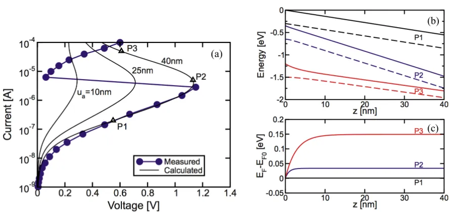
Figure 2.2: I-V characteristics of a PCM cell [8]
The amorphous state I-V curve shows two different regimes. At low bias, the resistance is fairly high. However as the voltage reaches a threshold value Vt, the amorphous material switches from a highly
resistive to a highly conductive state. The current rapidly rises with this voltage snap-back. Even after switching, the material is still amorphous. Phase transition to the crystalline state occurs only by further increasing the current. In this region, Joule heating is high enough to cause the temperature to exceed the glass transition temperature (Tg) but not Tm. Now if the current is reduced at a slow enough
rate to allow the material to cool, it crystallizes into a low resistance state. (It should be noted that the use of the term threshold voltage in this context is different from that used to turn on a MOSFET).
20
The electrical resistivity, ρ of the two phases differs by orders of magnitude. The resistance of the two memory states ranges from a few kΩ in the low resistance ON state, referred to as SET state to some
MΩ in the high resistance OFF state also know as RESET state [3].
In order to read the memory bit, a very low voltage, which essentially causes no joule heating, is used. In the SET state, a few mV of voltage applied across the cell generates 50-100 µA of current [8]. This evaluates to logic 1. However if the same bias is applied across the cell in RESET state then the resulting current generation in not enough to trigger the amplifier used to sense the current flowing through the cell. Hence this evaluates to logic 0. The read operation is possible in 50 ns [8].
2.3 Physical Principles Underlying PCM
As discussed in the preceding section, PCM device operation comprises of two major processes: amorphous-crystalline phase transition and threshold switching. The underlying physics is summarized in the sections below.
2.3.1 Amorphous-Crystalline Phase Transition
Consider a crystalline chalcogenide material. When it is heated, the material will start to melt at the solidus temperature Tsol illustrated in Fig. 2.3 and become completely molten at Tm. As the material
cools from the liquid state, it may transform back into the lower energy crystalline state and undergo a sharp change in volume. On the other hand, if the characteristic time constants of the crystallization process are slow compared to the cooling rate, the material may bypass crystallization and become a supercooled liquid. On further cooling the material enters into a glassy state at the glass transition temperature Tg. For temperatures below Tg, the ability of the system to rearrange itself becomes long,
21
also changes with the cooling rate as illustrated in Fig. 2.3. Conversely, when the amorphous material is heated to a temperature between Tg and Tm, it will start to crystallize. This is because; the
speed of the crystallization process is determined by a combination of the mobility of the atoms and the free energy difference between the starting and ending phases [14]. At Tm, the liquid and
crystalline states are in equilibrium and hence the free energy difference is zero. This implies that the maximum crystallization rate will occur at an intermediate temperature between Tg and Tm.
Figure 2.3: Schematic of volume-temperature variation of a PCM material showing different possible phase
transitions [14]
2.3.2 Band Structure for Chalcogenide Semiconductors
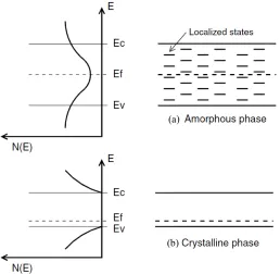
22
[image:44.612.184.442.200.452.2]
crystalline semiconductors [16]. This is because deep states tend to be highly localized, while mobility increases for energies approaching the conduction or valence bands. The large concentration of localized states causes the Fermi level to be pinned at about midgap in the amorphous chalcogenide. This results in a relatively large activation energy and high effective resistivity [17].
Figure 2.4: Schematic band diagrams and density of states as a function of energy of chalcogenide material for
(a) amorphous phase, (b) crystalline phase [15]
Crystalline chalcogenides such as Ge2Sb2Te5, GeTe, generally display small activation energy for
conduction, which is compatible with a selfdoping behavior, probably due to point defects (e.g., vacancies) in some Te compounds [16].
2.3.3 Conduction in the Crystalline Phase
In the crystalline phase, Ge2Sb2Te5 appears as a relatively low band gap, doped semiconductor,
23
used to describe electrical conduction in the crystalline phase, by applying the standard semiconductor theory [16]. This accounts for the behavior exhibited by the I-V curve in the crystalline phase as shown in Fig. 2.2.
In order to completely describe electrical conduction in phase change memory, it is essential to consider conduction in states, which display resistance values between the SET and RESET states. These intermediate states comprise of a mixed amorphous crystalline phase. Electrical conduction in this mixed-phase volume can be explained by percolation of carriers through dispersed low-resistivity crystalline grains [16]. Figure 2.5 shows two different mixed-phase states. State A is characterized by an incomplete percolation path, while state B is distinguished by a complete percolation path through low-resistivity crystalline grains. In state A, a small amorphous barrier limits the electrical current, and this accounts for the relatively large values of resistance and activation energy. For the case of state B, no amorphous barrier exists. Hence the activation energy for this state is the same as that of the bulk crystalline phase (SET state). However, the resistance still remains higher than the SET state due to geometrical effects, namely a small cross section and a relatively large percolation length through the mixed phase [16].
Figure 2.5: Schematic of two different mixed-phase configurations, characterized by an incomplete (State A) or
24
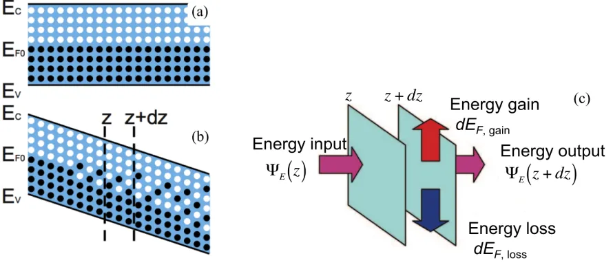
2.3.4 Conduction in the Amorphous Phase
[image:46.612.187.445.172.383.2]Figure 2.6 shows I-V characteristics as a function of temperature, for a PCM cell with TiN bottom contact and GST phase-change layer [17].
Figure 2.6: Measured I-V characteristics for amorphous GST at temperature T = 25, 45, 65 and 85˚C [17]
During the I-V measurement, the voltage sweep is always stopped below the threshold voltage Vt to
avoid threshold switching and consequent phase transformation due to Joule heating. It is observed that the I-V curves are linear for small applied voltages (< 0.3 V), and exhibit an exponential behavior at higher voltages. For the device in Fig 2.6, the threshold voltage is observed to be around 1.6 V (not illustrated) [17], and hence the region of the I-V curve shown in the figure is referred to as the sub-threshold region. It is ascertained that for increasing temperature, the current strongly increases due to the relatively large activation energy EA of conduction in chalcogenide glasses [17]. However, the
25
V = 0.4, 0.7, and 1 V, respectively. This behavior is commonly observed for trap-limited conduction such as the Poole-Frenkel (PF) mechanisms, where the applied electric field lowers the potential barriers, hence the activation energy for conduction [16-18]. As schematically shown in Fig. 2.7(a) and (b), Poole-Frenkel conduction is due to carriers (electrons in the figure) being thermally emitted from one trap to the conduction band and then captured by another trap [17]. In this figure, the energy barrier between two localized states, equal to
€
Δφ
( )
0 for zero applied voltage (Fig. 2.7(a)), is lowered to a value€
Δφ
( )
V by the application of a voltage V (Fig. 2.7(b)).
Figure 2.7: Schematic for sub-threshold conduction via localized states. (a) Electrons trapped at donor-type
traps confined by potential Δφ(0) at zero bias, (b) drop in potential barrier to Δφ(V) with application of voltage,
V > 0 [17]. (c) Profile of electron potential energy along minimum path between localized sates S1 and S2, with
electric field F = 0 (top) and F = 0.5 MV cm-1 (bottom) [19]
26
by (ii). Also shown is a third mechanism (iii), obtained by a combination of thermal emission and tunneling, namely thermally assisted tunneling. This consists of a thermal excitation within S1 to an energy level E below EC, followed by tunneling through the potential barrier seen at E [19]. While the
probability of reaching E is exponentially decreasing with E, the probability of tunneling through the barrier may be significantly higher than the tunneling probability for a 'cold' electron at the trap level ET indicated in Fig. 2.7(c) [19]. The combined transport due to thermally activated PF and tunneling
accounts for the strong temperature dependence of the current in Fig. 2.6 [16]. For PF conduction, the voltage dependence of the current can be expressed as [18],
€
I =IPFe βPFV1 2
(2.1) where
€
IPF and
€
βPF are constants. However (2.1) applies to emission from an isolated trap to the
conduction band and assumes that the nearest neighbor traps are still far enough from the trapped electron so that their contribution to the potential profile can be neglected [18]. This situation is therefore completely different from the physical picture in Fig. 2.7(a), (b) and (c), where traps are closely interacting as a result of a large density of traps in the glassy material. In order to analyze the impact of a different distances between traps on the shape of the I−V curve, Ielmini and Zhang [18] calculated the potential profile between two traps with variable intertrap distance
€
Δz. They determined that the change of the barrier height (barrier lowering) for a trapped electron depends linearly on the applied electric field F for small
€
Δz while a transition to a square root dependence on the field is found for increasing
€
Δz as the traps become more and more independent. Since the electron thermal emission current is exponentially dependent on the barrier lowering, it is concluded that, for sufficiently high trap density and a correspondingly short intertrap distance the current will obey [18],
€
I=I PFʹ′ eβPFʹ′V (2.2)
where
€
ʹ′
I PF and
€
ʹ′
βPF are constants. The linear dependence of barrier lowering on the applied voltage can
27
constant and experiencing a negligible shift upon a voltage increase [18]. As a result, the barrier change can be approximated as [18],
€
ΔU≈ −qFΔz
2 =−qV
Δz
2ua
(2.3)
where q is the elementary charge and ua is the amorphous chalcogenide thickness. Thus, the energy
barrier
€
Δφ
( )
V can be expressed as [16],
€
Δφ
( )
V =Δφ( )
0 +ΔU=E Cʹ′−EF0−qVΔz
2ua
(2.4)
where
€
ʹ′
E C is the conduction band mobility edge and EF0 is the equilibrium Fermi level. The mobility
edge is used instead of the proper band edge in order to take into account the tunneling contribution [19].
The average electron velocity can be expressed as the intertrap spacing divided by the average transfer time between two traps under the enhancement of the applied electric field. The transfer time in the same direction of the electrostatic force (i.e. forward time) is estimated as [18],
€
τ→=τ0exp
Δφ
( )
V kT ⎛ ⎝ ⎜ ⎞ ⎠⎟ =τ0exp
ʹ′
E C−EF0−qV
(
Δz 2ua)
kT ⎛ ⎝ ⎜ ⎞ ⎠⎟ (2.5)
where τ0 is the characteristic attempt-to-escape time for the trapped electron (typically in the range of
10-13 - 10-14 s). The corresponding forward current
€
dI→ can be obtained as [16],
€
dI→=qAnT
( )
E Δzτ→
dE=qAnT
( )
E Δzτ0
exp −E Cʹ′−EF0−qV
(
Δz 2ua)
kT
⎛
⎝
⎜ ⎞
⎠
⎟dE (2.6)
where A is the area of cross section of the amorphous region, and nT(E)dE is the concentration of
28
opposite to the electrostatic force [18]. The reverse flow of electrons will be significant at small fields. The reverse current
€
dI← can be obtained as [16],
€
dI←=qAnT
( )
EΔz τ0
exp −E Cʹ′−EF0+qV
(
Δz 2ua)
kT⎛
⎝
⎜ ⎞
⎠
⎟dE (2.7)
where the barrier lowering is replaced by a barrier increase, by the same amount but opposite sign. Therefore, the net current is given by [18],
€
dI=2qAnT
( )
E Δz τ0exp −E Cʹ′−EF0
kT ⎛ ⎝
⎜ ⎞
⎠
⎟sinh qV kT
Δz 2ua ⎛
⎝
⎜ ⎞
⎠
⎟dE (2.8)
Here the density of localized electrons is expressed by the Maxwell- Boltzmann statistics as [18],
€
nT
( )
E =NT( )
E exp −E−EF0 kT
⎛ ⎝
⎜ ⎞
⎠
⎟ (2.9)
where NTis the trap density. Thus from (2.8), the current I can be obtained by integrating over the
entire distribution of electron traps, i.e., above EF0, resulting in [16],
€
I=2qANT, tot Δz τ0
exp −E Cʹ′ −EF0 kT ⎛ ⎝
⎜ ⎞
⎠
⎟ sinh qV kT
Δz
2ua ⎛
⎝
⎜ ⎞ ⎠
⎟ (2.10)
where NT,tot is the densit
![Figure 1.1: Quantity trend of EEPROM, NOR Flash, NAND Flash and electronic system [1]](https://thumb-us.123doks.com/thumbv2/123dok_us/49616.4503/23.612.145.488.336.551/figure-quantity-trend-eeprom-flash-nand-flash-electronic.webp)
![Figure 1.2: NVM penetration rate in electronic systems [1]](https://thumb-us.123doks.com/thumbv2/123dok_us/49616.4503/24.612.99.537.146.407/figure-nvm-penetration-rate-in-electronic-systems.webp)
![Figure 1.4: (a) Cost-flexibility plane comparison of NVM technologies [2], (b) NOR+NAND Flash revenue [3]](https://thumb-us.123doks.com/thumbv2/123dok_us/49616.4503/25.612.174.458.202.365/figure-cost-flexibility-plane-comparison-technologies-flash-revenue.webp)
![Figure 1.6: Schematic cross-sections and circuit diagrams for NOR and NAND flash memory [5]](https://thumb-us.123doks.com/thumbv2/123dok_us/49616.4503/26.612.88.532.304.387/figure-schematic-cross-sections-circuit-diagrams-nand-memory.webp)
![Table 1.1: Comparison between Flash and Emerging NVM Technologies [15, 16]](https://thumb-us.123doks.com/thumbv2/123dok_us/49616.4503/31.612.88.528.93.683/table-comparison-flash-emerging-nvm-technologies.webp)
![Figure 2.6: Measured I-V characteristics for amorphous GST at temperature T = 25, 45, 65 and 85˚C [17]](https://thumb-us.123doks.com/thumbv2/123dok_us/49616.4503/46.612.187.445.172.383/figure-measured-i-v-characteristics-amorphous-gst-temperature.webp)
![Figure 2.11: Typical compositions of phase change materials [14]](https://thumb-us.123doks.com/thumbv2/123dok_us/49616.4503/58.612.96.540.73.338/figure-typical-compositions-phase-change-materials.webp)