City, University of London Institutional Repository
Citation:
Chalashkanov, N. M., Dodd, S. J., Dissado, L. A. and Fothergill, J. (2014).
Re-examination of the dielectric spectra of epoxy resins: Bulk charge transport and interfacial
polarization peaks. IEEE Transactions on Dielectrics and Electrical Insulation, 21(3), pp.
1330-1341. doi: 10.1109/TDEI.2014.6832281
This is the unspecified version of the paper.
This version of the publication may differ from the final published
version.
Permanent repository link:
http://openaccess.city.ac.uk/3827/
Link to published version:
http://dx.doi.org/10.1109/TDEI.2014.6832281
Copyright and reuse: City Research Online aims to make research
outputs of City, University of London available to a wider audience.
Copyright and Moral Rights remain with the author(s) and/or copyright
holders. URLs from City Research Online may be freely distributed and
linked to.
City Research Online:
http://openaccess.city.ac.uk/
publications@city.ac.uk
Re-examination of the Dielectric Spectra of Epoxy Resins:
Bulk Charge Transport and Interfacial Polarization Peaks
N. M. Chalashkanov, S. J. Dodd, L. A. Dissado,
University of Leicester University Road Leicester, LE1 7RH
and
J. C. Fothergill
City University London Northampton Square London, EC1V 0HBABSTRACT
The dielectric properties of two amine cured bisphenol-A epoxy resin systems, Araldite CY1301 and Araldite CY1311 have been characterized using dielectric spectroscopy over the frequency range 1 mHz to 100 kHz. These two epoxy resin systems were chosen to allow the dielectric response to be studied from above and below the glass transition, as Araldite CY1311 is a modified version (with added plasticizer) of Araldite CY1301. The dielectric response was found to comprise both bulk and interfacial features. Above the glass transition temperature, two processes were identified, a low frequency process usually ascribed to interfacial polarization is shown to be a bulk process termed Quasi-DC (QDC) conduction and a dielectric dispersion usually taken to be a bulk process has been shown to be an interfacial effect.
Index Terms
—
Epoxy resins, Dielectric measurements, Dielectric polarization, Charge transport, Equivalent circuits, Interface1 INTRODUCTION
E
POXY resins are an important class of thermo-setting polymers used, for example, as the base resin in high voltage insulators. They are often used unfilled or mineral filled as a potting compound in electronic devices such as capacitors, power supplies and in gas insulated switchgear. Epoxy resin impregnated paper and glass fibre reinforced resins are used as the electrical insulation in high voltage bushings. Such equipment is expected to last ~40 years in service under continuous load and with thermal loadings up to 90 °C. Under ac conditions at a power frequency of 50 or 60 Hz, space charge accumulation is not significant and the internal electric fields are governed by the permittivity of the insulating material which is not significantly temperature dependent. However, with the future growth of high voltage DC links, to link existing ac power networks and for transmission of electrical power from off-shore wind farms, the use of epoxy based insulation for such purposes requires a re-examination of their electrical properties. There are two main reasons for this. Firstly, the internal electric field under DC conditions is dependent on the electrical conductivity which in turn is highly dependent on temperature [1]. Secondly, the accumulation of space charge and/or temperature profiles existing within the insulator could result in a re-distribution of the internal electric field leading to local regions in the insulator where the localelectric field exceeds the breakdown strength of the material. Furthermore absorbed moisture is known to influence the electrical properties [2] and play a significant role in electrical degradation and breakdown [3]. All these processes are therefore likely to have a significant impact on reliability and service life of the insulators under DC conditions.
The dielectric properties of diglycidyl ether of bisphenol-A (DGEBbisphenol-A) epoxy systems (in particular bisphenol-Araldite CY1301) have been studied previously using frequency-domain spectroscopy and several processes have been found to contribute to the overall spectrum [4, 5]. These processes were classified as low-, mid- and high frequency according to their characteristic frequency in the range 10-2 to 105 Hz. In [4] the low frequency process was attributed to DC conduction, the mid-frequency dispersion was related to the glass transition temperature and recognised as α-relaxation and no particular interpretation was given to the high frequency process. However, no account was taken of the level of absorbed moisture in the samples used in this work. Similar interpretations for the low frequency process were proposed in [2, 5], where this process was attributed to either DC conduction (at low temperatures and low levels of absorbed moisture) or quasi-DC (QDC) charge transport (at high water content and high temperatures). In this case, the origin of the mid-frequency dispersion was related to the presence of ‘bound’ water molecules in the epoxy matrix
2
and again no interpretation was given for the high frequency process [5].
In this paper we examine the dielectric properties of two DGEBA based epoxy resin systems over the frequency range 4x10⁻⁴ to 105 Hz and at temperatures above and below the glass transition temperature of the fully cured resins. This aimed at a better understanding of their charge transport and dielectric dispersion characteristics and how temperature influences these properties. The two DGEBA based epoxy resins chosen for this study were Araldite CY1301 with HY1300 poly-functional amine based hardener which has a glass transition temperature (Tg) of approximately 50°C when fully cured and Araldite CY1311, using the same hardener with the same weight ratio, but containing flexiblizer to give a Tg of approximately 0°C when fully cured. Plaque samples of different thickness and samples with and without gold sputtered surfaces were used to distinguish between the bulk properties and interfacial effects. An equivalent circuit model encompassing the observed dielectric behaviour in terms of bulk and interfacial phenomena is proposed. The role of absorbed moisture on these characteristics will be the subject of a further paper.
2 RESPONSE FUNCTIONS
In this study we have analysed the dielectric response measured for our samples using the frequency dependent susceptibility functions predicted by the cluster theory [6, 7]. The cluster theory is a linear dielectric response theory. Such theories characterise the dielectric relaxation through a response function that describes the time dependent polarization current resulting from a step-application of an electric field [8]. According to the Dissado-Hill many-body theory [6], dielectric relaxation in solids and liquids can be viewed as the result of the cooperative connection of the motions of molecular dipoles or ions within and between clusters. In this theory the response function first involves the coupling of relaxation motions within the clusters followed by interactions of the motions in the different clusters comprising the whole ensemble. The intra cluster motions occur at frequencies higher than a frequency characteristic for the process (ωc), while the inter cluster motions occur at frequencies below ωc. The corresponding frequency dependent susceptibility is given by equation (1) [6]:
(
)
(
) (
( ) (
)
)
[
(
)
]
(
)
[
]
(
1)
1 2 1 0
i
1
;
2
;
1
,
1
F
i
1
2
1
1
− −+
−
−
−
×
+
−
Γ
Γ
−
+
Γ
−
Γ
=
p n p pn
m
n
n
m
m
n
m
n
α
ω
ω
ω
χ
ω
ω
χ
(1)
where Г(x) denotes the gamma function and 2F1( , ; ;) is theGaussian hypergeometric function. In the above expression the susceptibility χ(ω⁄ωp) is given as a function of the
reduced frequency ω⁄ωp. Here ωp is a frequency that is
characteristic of the specific relaxation phenomenon [6, 9] and is proportional to the loss peak frequency multiplied by
a numerical factor depending upon the power law exponents n, and m.
According to equation (1), a dielectric dispersion (loss peak) occurs when the parameters n and m are in the range,
1
0
,
1
0
<
n
<
<
m
≤
, with an asymptotic fractional power law frequency behaviour:( )
( )
( )
( )
( )
m pp n
ω
ω
ω
ω
χ
χ
ω
χ
ω
ω
ω
ω
χ
ω
χ
<
∝
′
−
′
∝
′′
>
∝
′
∝
′′
−for
0
for
1(2)
The Dissado-Hill functions, equations (1) to (3) are susceptibility functions that are exceedingly flexible. In the limit that m=1 and n=0 the theory reduces to the assumptions made by Debye and the function becomes the Debye function. When m=1 the function reduces exactly to the Cole-Davidson function. The Cole-Cole, Fuoss-Kirkwood, and Havriliak-Negami functions are closely approximated for exponents in the appropriate ranges [9]. We have used it here because its flexibility allows us to make a circuit model of the data without any preconceived assumptions regarding the specific form of relaxation peak function. In recent years the power law exponents of the Cole-Cole and Havriliak-Negami functions have received physical interpretation related to a self-similar (fractal) hierarchy of relaxation times associated with correlated cooperative motions of a dipole and its environment [10,11]. The reader is referred to [12] and references therein for further detail.
When the clusters are composed of ions or ionisable entities it has been shown in [7] that the dielectric response takes a form that can be expressed by equation (1) with
0
<
−
=
p
m
. This form of response was called low frequency dispersion (LFD) by Jonscher [13] and quasi-DC (QDC) conduction by Dissado and Hill [7]. It is characterized by two successive fractional power law responses (sometimes called constant phase angle (CPA) responses) at low and high frequency converting from one to the other at a characteristic frequency ωc (see also [14]):( )
( )
( )
( )
cp c n
ω
ω
ω
ω
χ
ω
χ
ω
ω
ω
ω
χ
ω
χ
<
∝
′
∝
′′
>
∝
′
∝
′′
− −for
for
1(3)
Such CPA and other fractional power law responses have been related to equivalent circuits with a fractal form [15, 16], i.e. ones exhibiting scaling hierarchy or dilation symmetry [17]. Such circuits may be found in both bulk responses [12, 15-17] and electrode responses produced by a fractal electrode surface [18]. In the cluster theory the high frequency CPA (
ω
>
ω
c) arises from the displacement of ions bound to a counter charge to form cluster dipoles (i.e. polarization of a cluster). At frequencies below ωc, ions3
percolation limit such that a connected path does not extend from electrode to electrode [20, 21]. The value of the low frequency power exponent p is governed by the dimension of the structure on which the ions move and that of the ion-walk on that path [16], with the incoherent diffusion value of
p
=
0
.
5
being a lower bound. In many instances a value of p that is very close to 1 is found and the response is distinguished from that of a DC-conductivity by the existence of the same frequency dependence in the real susceptibility as in the imaginary component. If charge transport between the clusters does not occur, the theoretical response function (forp
=
−
1
) reduces to an exact form resulting in a Cole-Davidson (see [8]) dielectric loss peak corresponding to the polarization of non-interacting clusters [22]. In recent work an explanation [23] has been provided for the low frequency fractional power law of equation (3) in terms of the slow retarding dynamics of carriers moving on a fractal structure that results in a representation with the form of a self-similar electrical circuit. However it should be noted that it is not possible to fit the data presented here by a single power law (CPA) response, i.e. the high frequency behaviour of equation (3) is also required.It should be noted that the susceptibility function defined above (equation (1)) describes an isolated dielectric response. However here, as in most materials, a number of processes are combined to give the complete response as measured experimentally. In particular, in this work, it is necessary to combine a QDC response with a dielectric relaxation loss peak and a DC conduction in order to fit data to theory. The contribution of each process has been separated and analyzed, and we will show evidence to the effect that the QDC process is a bulk mechanism that can occur in a ‘neat’ epoxy resin i.e. without any filler particles, while the relaxation loss peak is produced by interfacial features that can be produced for example by a blocking contact at the electrodes. This is contrary to the opinion sometimes expressed in the literature that large dispersions at low frequency are always associated with interface effects (and often removed from the observed response for that reason [24]. In [25] χ’’α χ’ α ω-p at low frequencies is regarded as an interface effect. References [18, 26, 27] describe how the power law can be produced by a fractal interface. Here we point out that the same power law behaviour at low frequencies can be produced by a bulk QDC transport process that has fractal transport features [16]. We will also show that loss peak dispersions observed in materials dominated by ion transport cannot be necessarily associated with bulk molecular relaxation mechanisms [28-30] as these dispersions are shown to be caused here by interface effects.
3 EXPERIMENTAL
3.1 SAMPLE PREPARATION
The epoxy systems were prepared by mixing the base epoxy resin (CY1301 or CY1311) with 30% by mass amine hardener Aradur HY1300GB. To do this, the liquid epoxy
resin and hardener were first degassed in a vacuum oven in separate beakers for 10 min at 30 to 40 °C. Then they were mixed together at 40 °C using a magnetic stirrer on a hot plate for 10 min. After mixing, the mixture was degassed in the vacuum oven for 10 min to remove any air bubbles trapped during the mixing stage. The epoxy samples were then cast in aluminium moulds to produce plaque samples in two thicknesses: 0.7±0.1 mm and 1.7±0.1 mm. The epoxy samples were left to cure in the moulds for two days at room temperature (~20 °C). They were then post-cured for 1 h at 100 °C under vacuum to ensure completion of the cure reaction before slowly cooling down to room temperature. Once taken out of the moulds, they were cut into disks of diameter of 70 mm and the thicknesses of the samples were measured with a micrometer. The sample-to-sample variation in thickness was determined to be within ±0.1 mm. The samples, assumed dry at this stage, were then weighed using an analytical balance of 0.1 mg precision before being stored in sealed containers under controlled temperature (20 °C) and humidity conditions (using saturated salt solutions) in order to obtain reproducible values of absorbed moisture of 0.6% by mass for all samples before the dielectric tests.
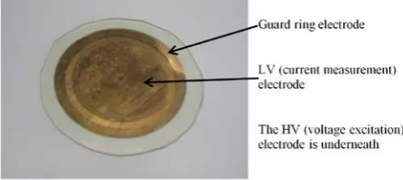
Some of the samples were sputter-coated with gold in order to produce a direct electrical contact between the measurement cell electrodes and the sample. The sputter coater used was an EMITECH K550X. The coating was made under a stable vacuum of 0.1 mbar with argon as a process gas. The deposition current was 25 mA and the corresponding deposition rate, as specified by the manufacturer, was 7.5 nm/min. The total time for sputtering on one side of a sample was set to be 8 min and the resultant thickness of the gold layer was therefore estimated to be 60 nm. This thickness was sufficient to produce a uniform layer of gold on the sample surface, which was checked by an optical inspection. The gold was sputtered on one side using a circular mask of diameter 60 mm to form the “high voltage” (HV) electrode – i.e. the electrode to which the excitation voltage was applied - and then subsequently on the other side using the same 60 mm mask and an additional ring mask of 50 mm external diameter and 5 mm width to match the size of the guard and measurement (LV) electrodes of the measurement cell. A photograph of a sample with sputter-coated gold guard, LV and HV electrodes is shown in Figure 1. Note that in this photograph the guard and the LV electrodes are on the top side of the sample while the HV electrode is on the bottom side.
[image:4.612.333.555.595.694.2]4
3.2 DIELECTRIC MEASUREMENTS
A bespoke test cell, shown in Figure 2, was used for the dielectric measurements. This was designed to enable dielectric measurements to be taken under controlled temperature and humidity environmental conditions in order to maintain a stable level of absorbed moisture in the samples over a sufficient length of time to take the dielectric measurements. A three-electrode configuration was used for the measurements. The three electrodes were made from brass and the surfaces in contact with the sample were sputter coated with gold to ensure good electrical contact. The HV electrode was connected to the voltage generator side of the dielectric interface and current flow through the material measured using the LV electrode, connected to the current input of the dielectric interface. The diameter of the LV electrode was 44 mm; hence the values for the empty cell capacitance were 19 and 8 pF for the thinner and thicker samples, respectively. The guard electrode was used to eliminate the influence of surface currents, which may otherwise obscure the bulk response of the material, by diverting these currents to earth. The weight of the guard electrode was used to load a compression spring and provide mechanical force to the LV measurement electrode to ensure good mechanical and electrical contact with the epoxy sample. In this way, the volumetric expansion of the epoxy sample, which occurs when samples are heated to higher temperatures, was accommodated. In order to control the measurement temperature, the measurement cell was placed in a Genlab oven with a Eurotherm 2204 temperature controller. The temperature was kept within ±0.5°C of the target level by the controller during each measurement. A saturated salt solution contained within the cell was used to maintain the humidity in the cell to the same level that was used for sample storage. The values of the temperature and relative humidity during the experiments were monitored by a temperature and humidity probe Digitron 2020R placed in the cell using a gland located in the side wall of the sealed chamber. The temperature and humidity lags of the system were measured and care was taken to ensure enough time was given for the sample to reach equilibrium before measuring its impedance. In order to eliminate absorbed moisture dependency in this work, all samples were tested with a moisture content of 0.6% by mass as determined by mass measurement using an Analytical Balance prior to each experiment.
[image:5.612.324.573.53.212.2]Connections from the measurement electrodes and the dielectric analyser were made using coaxial cable via bulkhead connectors attached to the cell’s metal enclosure (see Figure 2) ensuring that stray capacitive currents are diverted to earth and not measured by the dielectric analyser. The complex impedance of the samples was measured as a function of frequency using a Solartron 1255HF frequency response analyser (FRA) and a Solartron 1296 dielectric interface. In this technique, the amplitude and phase of the electric current flowing in the sample due to an applied AC electric field between two parallel plate electrodes is measured [13].
Figure 2. A photograph of the measurement cell
.
For consistency, the same magnitude of applied electric field was used for the samples having different thicknesses. The magnitude of the applied voltage was therefore scaled with the sample thickness; 1.5 and 0.6 V rms for samples with thicknesses of 1.7 and 0.7 mm, respectively. For all samples, the dielectric response was measured over the frequency range 3.710-4 to 1.0105 Hz. The data were acquired over two cycles of integration at each frequency and 7 data points per decade were taken over the entire frequency range. The dielectric properties of CY1311 samples were measured over the temperature range 20 to 60
°C and the corresponding temperature range was 20 to 80
°C for CY1301 samples. Hence, the CY1301 samples were measured both below and above their glass transition temperature, while the CY1311 samples were tested at least 20°C above their glass transition temperature.
4. RESULTS
4.1. SAMPLES WITHOUT SPUTTER COATED GOLD CONTACTS
5
dispersion where an increment in the real part of the permittivity of nearly an order of magnitude is observed as well as a corresponding peak in the imaginary part of the permittivity indicating a possible dielectric dispersion. The dielectric spectra above and below the glass transition temperature are therefore fundamentally different with dielectric relaxation processes that only occur in this frequency range when the epoxy resin is in a flexible state. It is tempting at this stage to conclude that the data obtained at 80°C indicates that at low frequencies, the dielectric properties are dominated by a Maxwell-Wagner type interfacial polarization while the mid frequency response is dominated by a dielectric dispersion due to dipolar orientation of permanent dipoles attached to the polymeric molecular chains as is often reported in the literature [31]. However as we shall see, there is another interpretation for this type of dielectric response which will become more obvious when we consider the dielectric properties of the flexible CY1311 epoxy resin in the next section.
Figure 3. Real (solid markers) and imaginary (open markers) parts of the relative permittivity of epoxy resin CY1301 at temperatures 20°C(), 40°C(), 60°C() and 80°C(), sample thickness 1.7mm.
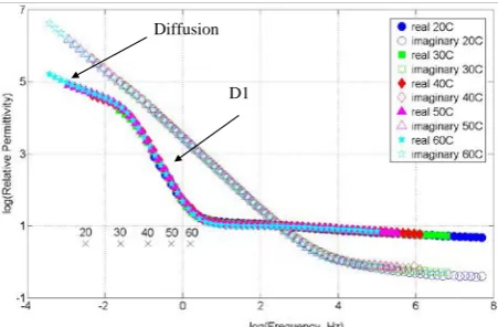
4.1.2. Dielectric response of Araldite CY1311. The dielectric response of CY1311 epoxy resin was measured at temperatures between 20 and 60°C in 10°C steps. As the glass transition temperature of Araldite CY1311 is 0 °C; all spectra were therefore obtained at different temperatures above the glass transition temperature. As there is no phase change of the epoxy resin over this temperature range (i.e. it remained in the flexible state) it was possible to obtain a master plot of the dielectric spectra by lateral shifts of the dielectric data obtained at each temperature when plotted on log-log axes. A master plot of the dielectric response of a CY1311 sample is shown in Figure 4. The dielectric spectra closely resemble the response of CY1301 at 30°C above its Tg, and shift in frequency with increasing temperature. The locus of the translations required to bring the data from each temperature into coincidence is given as a set of points below the master curve and the spectra are normalised with respect to the data obtained at the highest temperature, 60°C. The frequency shifts required were found to decrease with increasing temperature.
Figure 4. Master plot of the temperature dependence of CY1311 sample, absorbed moisture 0.6%, thickness 1.7mm, data normalised to 60 °C.
At the low frequency end of the spectra, the real (
ε
'
r) andthe imaginary (
ε
r′′
=
χ
r′′
) parts of the permittivity are nearly parallel to each other on a log-log representation and follow a fractional power law dependence on frequency. At the high frequency end of the spectra the real and imaginary parts are also parallel and follow another fractional power law. This form of response is defined in equation (3) and represents quasi-DC (QDC) charge transport. In the mid-frequency range another process appears to take place which is characterized by a dielectric increment and a loss peak and represents a dispersion process that can be described by equation (2). The dielectric dispersion process (D) is superimposed on the QDC response. It can be seen from Figure 4 that the characteristic frequencies of both processes scale with temperature in the same way, hence it was possible to construct a single master plot of the dielectric response over the entire frequency range. This suggests that the activation energies and hence the physical origins for the two processes are the same.4.1.3. SAMPLE THICKNESS DEPENDENCE OF THE DIELECTRIC PROPERTIES OF ARALDITE CY1311. Figure 5 shows dielectric spectra obtained from four CY1311 samples conditioned under the same humidity environment.
Figure 5. Thickness dependence of the dielectric response, CY1311 resin, 20 °C.
1E-4 1E-3 1E-2 1E-1 1E+0 1E+1 1E+2 1E+3
0.0001 0.01 1 100 10000
R
elat
ive
P
er
m
it
tivit
y
Frequency, Hz
Low frequency response
Mid-frequency response
High frequency response
QDC
D εr’
εr”
QDC
6
[image:7.612.324.550.53.201.2]Two of the samples had a thickness of 0.7 mm and the other two had a thickness of 1.7 mm. It can be seen from Figure 5 that the dielectric response of samples of the same thickness was essentially identical indicating good experimental reproducibility.
The four spectra are also consistent with the dielectric response master curve described above. The only discrepancy between the four spectra is in the increment of the real part of permittivity associated with the dispersion process D. It has explicit thickness dependence with the thicker samples having greater increment in the real part of the permittivity. This behaviour is a consequence of converting a thickness-independent capacitance, such as may originate in an electrode interface, into relative permittivity using the cell constant. Thus the origin of the D process appears to be an interfacial response. At the very low and the very high frequencies the four spectra practically coincide, which suggests that the relative permittivity of the QDC process is independent of the sample thickness and therefore can be identified as a bulk process. A similar dielectric response (QDC and superimposed mid-frequency dispersion) was observed in the case of hydrated biopolymers [32], where the mid-frequency dispersion has been found to be electrode dependent and hence interfacial while the QDC process has been identified as a bulk response.
4.2. SAMPLES WITH SPUTTER COATED GOLD CONTACTS
A CY1311 sample with sputter coated gold electrodes was conditioned in the same humidity container as the samples previously described. The dielectric response of the sample before the gold coating was similar to that shown in Figure 4. A master plot of the response after the gold coating procedure is shown in Figure 6. Once again it was possible to obtain a single master plot over the entire frequency range. The locus of the translation point is given below the curve and it is similar to that presented in Figure 4 for the uncoated samples. In the high frequency end of the spectra there are no differences between the responses shown in Figures 4 and 6. However, the dielectric response has changed quite significantly in the mid and low frequencies. The dispersion process D has been replaced by a new dispersion process D1 having a significantly lower characteristic frequency (ωp of equation(2)) and a dielectric increment of three orders of magnitude, much larger than the dielectric increment for D. At the very low frequencies the real part of permittivity increases with a fractional power law whose exponent is approximately equal to -0.5 suggesting that a possible diffusion process (χ’(ω) ∝χ”(ω)∝
ω-0.5
) [8] has become large enough to dominate the frequency dependence of ε’(ω), the transport process however continues to dominate ε”(ω ). A similar dielectric response was observed above Tg, in the case of a CY1301 sample with sputter coated gold electrodes which is not shown here for brevity.
Figure 6. Master plot of the temperature dependence of a CY1311 sample with sputter coated gold electrodes on it, thickness 1.7 mm. Data normalized to 60 °C.
5. EQUIVALENT CIRCUIT MODELLING
In the case of samples without gold coating, the dielectric measurements above Tg were analysed in terms of an equivalent circuit model [33]. Initially all processes were considered to be independent and additive towards the total response in a parallel circuit configuration, as shown in Figure 7. Four processes are represented: two Dissado-Hill components (see equation 1), DH1 modelling the dielectric dispersion D with the asymptotic power law dependence given by equation (2), and DH2 modelling the QDC response with the asymptotic power law dependence given by equation (3), a DC conductance (G) and a frequency independent capacitance (C∞). Each Dissado-Hill component is fully described by four parameters: characteristic frequency, ωp (for a loss peak) or ωc (for QDC
process) amplitude, χ0and the two power law exponents, m
[image:7.612.332.562.617.688.2](or –p) and n-1, characterizing the frequency dependence below and above the characteristic frequency of the particular process. Hence, the total number of free parameters to fit the data according to the equivalent circuit shown in Figure 7 is ten (four for each Dissado-Hill component, one for the DC conductance and one for the frequency independent capacitance). A non-linear least squares algorithm was used as a fitting routine. The frequency independent capacitance (C∞) is likely to be due to electronic polarization. At optical frequencies the relative permittivity is equal to the square of the refractive index. The value of the refractive index for epoxy resins is reported as 1.515 [34]. We have therefore assumed that εr∞ = 2.3 and hence we have used values for C∞ of 44 and 18 pF for the thinner and thicker samples, respectively.
Figure 7. Initial equivalent circuit model for fitting the data [33]. D1
7
[image:8.612.61.562.60.288.2]The fit to the experimental data using the equivalent circuit of Figure 7 was found to be good and a typical example is shown in Figure 8, where the experimental data points are represented by the markers and the overall fitted response is plotted with thickened lines. The individual components of D, QDC, G and C∞ contributing to the overall measured dielectric response are also plotted in Figure 8. The dielectric response at the lowest frequencies and at the highest frequencies is dominated by the asymptotic power law dependence of the QDC process. The dispersion (D) is superimposed on the QDC response in the mid-frequency range. The DC conductance (G) is important only at low frequencies. It affects only the imaginary part of the complex capacitance and leads to a small difference in the measured power law exponent for the imaginary component of the capacitance (and hence permittivity) in the lowest frequency range measured. The contribution of C∞ is significant at the highest frequencies measured as an additive term to the real part of the complex capacitance. The values of the equivalent circuit parameters used to fit the experimental data over the range 20 to 60°C are given in Table 1. The amplitude of the D process remained fairly constant (~600 pF) over this temperature range. The low frequency power law parameter of D had a value of 1.0 over the full temperature range but large fitting error as the low frequency data are dominated by the QDC process. Only the lower tolerance limit has physical significance when the power law parameters have value of 1. The high frequency power law parameter decreased from -0.91 to -1.00 as the temperature increased and hence at 40°C and over the D process resembled a Debye like response (which displays asymptotic slopes of +1 and -1). The characteristic frequency of the dispersion process, D, increased significantly with increasing temperature consistent with the frequency shifts in the master plot (Figure 4).
Table 1. Values of the fitted parameters and 95% confidence intervals for the equivalent circuit model.
Param. Temperature
20 ºC 30 ºC 40 ºC 50 ºC 60 ºC Ampl.
dispersion process D, pF
561 ±22
666 ±33
600 ±57
530 ±50
642 ±65
Low freq. slope (m) of D
1.0 ±0.1
1.0 ±0.2
1.0 ±0.3
1.0 ±0.3
1.0 ±0.3
High frequency slope of D (n-1)
-0.91 ±0.01
-0.95 ±0.02
-1.0 ±0.02
-1.0 ±0.02
-1.0 ±0.02
Dispersion process char. frequency, Hz (ωp)
0.028 ±0.004
0.15 ±0.02
0.81 ±0.18
2.6 ±0.7
6.9 ±2.3
QDC amplitude, pF
90 ±3
138 ±3
144 ±4
143 ±6
161 ±11
Low frequency slope of QDC (-p)
-0.916 ±0.006
-0.954 ±0.001
-0.955 ±0.001
-0.958 ±0.002
-0.968 ±0.003
High frequency slope of QDC (n-1)
-0.090 ±0.001
-0.095 ±0.001
-0.095 ±0.002
-0.084 ±0.004
-0.084 ±0.006
QDC char. frequency, Hz (ωc)
1.27 ±0.05
12.2 ±0.3
77 ±3
345 ±20
798 ±65
C∞, pF 18 18 18 18 18
DC conduct., pS
48 ±1
142 ±6
1303 ±66
8708 ±287
[image:8.612.317.571.340.717.2]8
The amplitude of the QDC response shows slight temperature dependence from 90 pF at 20 °C to 161 pF at 60°C whereas the low and high frequency power law slopes remained relatively independent of temperature having values of -0.95 and -0.09 respectively. The QDC characteristic frequency increased significantly with temperature from 1.2 Hz at 20 °C to 798 Hz at 60 °C and again was consistent with the frequency shifts in the master plot. The DC conductance, G, was also found to be temperature dependent, having values of 48 pS at 20 °C and 29200 pS at 60 °C, whilst setting the frequency independent capacitance, C∞, to the square of the refractive index, was found to result in a good fit to the results obtained.
Arrhenius plots of the characteristic frequency (fc) of QDC
and D and the magnitude of the DC conductivity are shown
in Figure 9. The values of the activation energy for the three processes calculated from the slope of the Arrhenius plots are 1.4±0.1 eV for the QDC process, 1.2±0.1 eV for the D dispersion and 1.4±0.1 eV for the DC conductance. The three activation energies agree within the uncertainty and hence this supports the evidence from the master plot that these three processes share the same physical origin.
Figure 9. Arrhenius plot of fc QDC process (), fc D () and DC
conductance(), CY1311 resin, sample thickness 1.7mm.
6. DISCUSSION
6.1. COMPARISON BETWEEN THE DIELECTRIC RESPONSES OF CY1311 AND CY1301 RESINS Figure 10 shows a comparison between the dielectric responses of CY1311 and CY1301 measured at the same relative temperature (~30 °C) above their respective glass transition temperatures. Before each measurement the two samples were conditioned in containers with a low environmental relative humidity. Although, the percentage moisture content was slightly different (0.2% relative difference in this case), Figure 10 demonstrates that the bulk QDC behaviour of the epoxy resins at nearly the same relative temperature above their glass transition temperature and with similar moisture contents give rise to dielectric behaviour which is effectively the same. Slight differences in the dielectric dispersion, D, are observed. Given that CY1301 and CY1311 have different chemical constituents (CY1311 contains a flexibilizer) and therefore a different cured molecular structure and cross-link density, the dielectric measurements show that the bulk electrical
properties are governed only by the relative temperature above Tg for samples containing similar amounts of absorbed water. The chemical constituents just determine the glass transition temperature of the final cured resin. It can be concluded that the dielectric response presented here, i.e. QDC and superimposed dispersion D, is representative for Bisphenol-A epoxy resins above Tg in general. A QDC charge transport was also observed in [35] in the case of Araldite LY556. The above results also suggest that as QDC is observed only at temperatures above the glass transition temperature, when the resin is in a flexible state, that bulk charge transport leading to the observed QDC behaviour is facilitated by segmental chain motions i.e. that charge transport occurs by the exchange of charge carriers between adjacent polymer chains when they have a particular conformation relative to each other.
Figure 10. Real (solid) and imaginary (open markers) of the relative permittivity of epoxy resin CY1301, thickness 1.7mm, at 80 °C () and CY1311, 30 °C ().
6.2. BULK AND INTERFACIAL PROCESSES Although the simple parallel equivalent circuit, shown in Figure 7, was successful in modelling the experimental data, it suffers from an inconsistency. If the D process is to be represented as an interfacial feature, i.e. as a blocking contact, then the D dispersion should be connected in series with the bulk QDC response in the equivalent circuit. Secondly, the equivalent circuit model cannot represent the sample thickness dependency that was observed in the dielectric response without changing the circuit parameters. For this reason the origins of the D dispersion were further investigated. An investigation of the electrode-sample contact was carried out by sandwiching a typical CY1311 sample between two glass plates. This sample had been conditioned in a container with a high relative humidity (75%), which facilitated the adhesion between the epoxy sample and the glass plates. The photographs shown in Figure 11a reveal three types of contact between the epoxy sample and the glass plates, namely no contact, single-sided, and double-sided contact.
The different types of contact can be distinguished by slight changes in colour of the reflected light due to the differences in the corresponding refractive indices of the materials in contact with the glass surface, either epoxy-glass or air-epoxy-glass. These different contact regions are due to slight variations in the sample thickness.
1E-1 1E+0 1E+1 1E+2 1E+3 1E+4
0.0001 0.01 1 100 10000
R
elat
ive
p
er
m
it
tivit
y
9
Figure 11a. Contact zones between an epoxy resin sample and two glass plates. The photographs are taken on both sides of the sample.
Figure 11b. Diagram illustrating poor sample contact, with parallel regions exhibiting bulk QDC and other parallel regions involving a blocking capacitance C and bulk QDC that give rise to the D dispersion in uncoated samples.
Such a complicated heterogeneous contact can be thought of as a parallel combination of regions of epoxy in perfect contact exhibiting a bulk QDC response and regions where an air-gap exists to block the passage of current at the sample surfaces as the origin of the D process with both the QDC and DC conduction combining to charge the capacitance of the air-gap. This is shown schematically in Figure 11b. This could explain the introduction of a parallel interfacial dispersion process (D) into the equivalent circuit and the ability of the resultant equivalent circuit to successfully fit experimental data.
The introduction of the sputtered gold coating on the epoxy surface effectively short circuits the blocking capacitance, C, and produces a homogeneous metal-epoxy electrical contact and therefore eliminates the D dispersion. A comparison between the dielectric spectra obtained at 60oC before and after the gold coating was applied is presented in Figure 12 for a CY1311 sample. The initial dispersion (D) with dielectric increment ε’ of approximately one decade was replaced by the new dispersion (D1) having a much higher dielectric increment of three decades but occurring at a much lower frequency. The shape of this new relaxation process closely resembles Maxwell-Wagner-Sillars (MWS) interfacial polarization, with the frequency
exponent q of the real part of the permittivity
ε
′
∝
ω
−q being greater than 1, over the frequency range 0.1 Hz to 1 Hz, see [8]. It is suggested that the sputtered gold electrodes create a nearly homogeneous electrical contact and thus eliminate the dispersion process (D), with the new dispersion (D1) attributed to a blocking effect of the sputtered gold layer to any ions that might be present in the bulk of the epoxy resin. The master curve shown in Figure 6 for the gold coated sample over the temperature range 20°C to 60°C shows that the process D1 also scales with the bulkQDC and hence both features arise from a common physical process. It is more likely that ions are involved in the QDC charge transport than other charge carriers considering the chemical composition of the epoxy resins and the values of the activation energy of the processes. It is suggested that the D1 process is the result of QDC ion migration in the bulk of the sample and build-up of these ions at the blocking gold/epoxy contact. Investigating the origin of the charge carriers involved in the bulk QDC process is a subject for future work.
Figure 12. Real (solid) and imaginary (open markers) of the relative permittivity of an epoxy resin sample CY1311, at 60 °C, before the sputter coating () and after the sputter coating (), thickness 1.7 mm.
6.3. MODIFIED EQUIVALENT CIRCUIT
The original parallel equivalent circuit (Figure 7) was modified to incorporate the effects of the sample-electrode contact. As discussed above, poor electrical contact between the sample and electrodes is the likely cause for the dispersion D in the case of the uncoated samples and interfacial polarization is the cause for the dispersion D1 in the case of the gold coated samples. These two situations are illustrated schematically in Figure 13.
Figure 13. Sample – electrode interface zone: (a) uncoated sample, (b) gold-coated sample (not to scale).
A modified equivalent circuit, shown in the inset to Figure 14, was used to model the dielectric data in the case of an uncoated sample. The aim of this analysis was to check whether the equivalent circuit would provide an appropriate representation of the physically observed behaviour and have sufficient degrees of freedom to encompass the range of dielectric data observed, thereby supporting the interpretation of the interfacial phenomena described above. The characteristic parameters of the processes fitted using the modified equivalent circuit are given in Table 2. In this case, the original Dissado-Hill dispersion element describing the mid-frequency dispersion, D, was replaced by a series network of a QDC component representing the
1E-1 1E+1 1E+3 1E+5 1E+7
0.0001 0.01 1 100 10000
R
elat
ive
P
er
m
it
tivit
y
Frequency (Hz)
D D1
10
bulk material (QDC1 in Figure 14) and a series blocking capacitance, Cs, representing the air-gap in the case of imperfect contact. A conductance, Gs, was inserted in parallel with Cs to represent surface conduction along the epoxy surface.
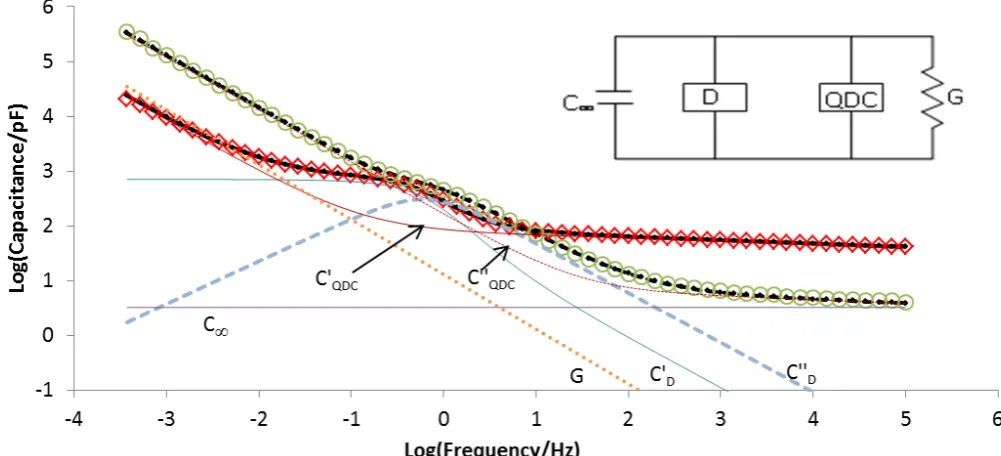
Figure 14. The modified equivalent circuit (inset) representing the dielectric data in the case of an uncoated sample and the individual contributions of each process in a log-log plot. Experimental data points: real capacitance (◊) and imaginary capacitance (○); fitted response as thickened lines, CY1311, absorbed moisture 0.6%, 50 °C.
Table 2. Values of the fitted parameters using the modified equivalent circuit
Parameter Sample
without gold coating (Figure 13)
with gold coating (Figure 14)
QDC1 amplitude, pF 115±10 1117±19
QDC2 amplitude, pF 103±8 -
Low frequency slope (p) -0.979±0.002 -0.996±0.001
High frequency slope
(n-1) -0.09±0.01 -0.093±0.006
QDC characteristic
frequency, Hz 1192±88 660±40
C∞ 18 18
G, DC conductance
(bulk), pS - 25750±800 Gs, DC conductance
(interface), pS 3500±900 - CS, Series capacitance,
pF 980±100 -
CB, Blocking
capacitance, µF - 0.29±0.02 Power Law Amplitude,
pF - 6300±2900
Power Law Exponent - -0.52±0.07
The bulk epoxy resin in good contact with the electrodes is represented by another QDC process (QDC2 in Figure 14) having the same characteristic frequency and power law exponents as QDC1 but a different amplitude. A frequency independent capacitance, C∞, is also included to account
for high frequency dielectric polarization of the epoxy resin. The equivalent circuit was fitted to data obtained from a CY1311 sample with absorbed moisture 0.6% and at a temperature of 50°C. In the fitting of the data the value of
C∞ was set to 18 pF in accordance with the previous model circuit of Figure 7.
An approximate calculation would suggest that the fitted value of Cs is reasonable. From Figure 11a, approximately
30% of the sample cell electrode does not appear to be in contact with the sample. With an electrode diameter of 44 mm (for the measuring electrode) the area in contact is therefore approximately:
(
3)
2 2m
00106
.
0
10
22
7
.
0
×
π
×
×
−=
.Assuming the air gap is approximately 10 µm (which would seem reasonable), then the capacitance, Cs, would be
940 pF. The value of 980 pF obtained from the circuit model is therefore reasonable.
In the case of gold coated samples, the modified equivalent circuit is shown in the inset to Figure 15. In this case CB, represents the blocking capacitance as a result of the formation of an electrical double layer, and the bulk epoxy is represented by the QDC process, a parallel DC conductance, G, and a frequency independent capacitance, C∞ (again fixed to a value of 18 pF). The charges (most likely ions) that take part in the QDC transport are not able to cross the gold layer and therefore accumulate at the gold interface, where they form a double layer and give rise to Maxwell-Wagner-Sillars (MWS) interfacial polarization (denoted by D1 in Figure 6). The characteristic frequency of this dispersion is determined by the magnitude of the QDC transport process and the series capacitance CB in a similar way to the relaxation frequency of a series conductance and capacitance circuit. The diffusion process that dominates at low frequencies (see Figure 6) can be related either to formation of a diffuse double layer [36] further away from the electrode or due to charge transport across the interface, which is facilitated by the field intensification in this region. This process is modelled by the power law component in parallel with CB. The results of the fitting programme are given in Table 2 for a CY1311 sample with absorbed moisture 0.6%, at a temperature of 50 °C.
If we assume that a significant proportion of the applied voltage is dropped across, CB, say 1 V, and that the field at
the electrode is moderated by Schottky emission, then it would be reasonable to assume that this field may be of the order of 107 V.m-1. This would then lead to a very approximate thickness of the blocking capacitance of 10-7 m (assuming the voltage is dropped linearly). If the permittivity at high frequencies is 2.3, then this suggests that the blocking capacitance should be of the order of 0.31 µF. The value found of 0.29 µF from Table 2 is therefore reasonable.
A comparison between the gold coated and uncoated sample shows that the characteristic parameters describing the bulk processes have similar values in both cases, while the value of CS(B) associated with the sample-electrode contacts vary by a few orders of magnitude (see Table 2). The small differences in the QDC low frequency power law (-p) and the characteristic frequency (ωc) can be attributed to changes in the sample that have taken place during the -1
0 1 2 3 4 5 6 7 8
-4 -3 -2 -1 0 1 2 3 4 5 6
L
o
g
(Ca
p
a
ci
tan
ce
/p
F)
Log(Frequency/Hz)
QDC QDC C∞
Cs Gs
1 2
CS
C∞ C'QDC
11
sputter coating procedure. The increased value of the DC conductance in the case of gold coated sample is due to increased contact area between the sample and the electrodes. The fitted value of the frequency independent capacitance, C∞, was the same in both cases.
Figure 15. The modified equivalent circuit (inset) representing the dielectric data in the case of gold coated sample and the individual contributions of each process in a log-log plot. Experimental data points: real capacitance (◊) and imaginary capacitance (○); fitted response as thickened lines, CY1311, absorbed moisture 0.6%, 50 °C.
7. CONCLUSIONS
We have shown that the dielectric response of bisphenol-A epoxy resins above their glass transition temperature can be characterized dielectrically by four main processes: QDC charge transport, a dispersion processes superimposed on it in the mid-frequency range, a frequency independent capacitance and a DC conductance. The electrical properties of the resins for a given level of absorbed moisture are governed only by the relative temperature above Tg, while the chemical constituents determine the glass transition temperature of the final cured resin. The dielectric data were analysed in terms of equivalent circuits in which the various elements represented physical attributes of the measurement scheme with components obeying the Dissado-Hill model for dielectric relaxation. This allowed the relative contributions of each process to the total spectrum to be quantified. We have shown that different equivalent circuits can fit the data with a similar accuracy and care therefore must be taken in the selection of an appropriate circuit. Only equivalent circuits which represent the physical nature of the measured system should be used to obtain the values of the parameters characterizing the processes involved.
The QDC charge transport was identified as a bulk process, while the various dispersion processes were shown to be interfacial features in the spectra due to an imperfect sample-electrode contact. This is contrary to previous interpretations in the literature where the dispersion process, D, was assumed to be a material property associated with α-relaxation and the QDC (low frequency dispersion) to be an interfacial process. The large difference in the spectra of uncoated and gold coated samples demonstrates that the interfacial features can have a major effect on the overall dielectric response and care is necessary to be able to extract
the bulk and interface characteristics from the analysis of dielectric data.
The QDC charge transport and the DC conductance were found to be thermally activated processes and the values of the activation energy were estimated in the range 1.0-1.5 eV. Therefore it is likely that the charge carriers involved in the QDC transport are ions, however a further work is required to confirm their nature.
The possibility of quasi-DC ionic transport and the corresponding build-up of space charge at the resin-metal interfaces have significant implications for the applicability of epoxy resin systems as electrical insulation materials. The local electrical field may increase above the breakdown strength of the material due to the presence of space charge at the interface and thus an electrical breakdown may be triggered. This is especially important if epoxy resin based materials are to be used as an electrical insulation for DC systems, where the long range charge transport will be facilitated due to the lack of polarity reversal, i.e. due to 𝜔𝑐> 𝜔 = 0.
REFERENCES
[1] L. A. Dissado and J. C. Fothergill, Electrical Degradation and Breakdown in Polymers, 1st ed., Peter Peregrinus Ltd, 1992.
[2] C. Zou , J. C. Fothergill and S. W. Rowe, “The Effect of water absorption on the dielectric properties of epoxy nanocomposites”, IEEE Trans. Dielectr. Electr.l Insul., Vol. 15, pp. 106-117, 2008. [3] J. V. Champion and S. J. Dodd, “An assessment of the effect of
externally applied mechanical stress and water absorption on the electrical tree growth behaviour in glassy epoxy resins”, J. Phys. D: Appl. Phys., Vol. 32, 305-316, 1999.
[4] V. Griseri, The effect of High Electric Fields on an Epoxy Resin, Ph.D. degree thesis, University of Leicester, Leicester, UK, 2000. [5] C. Zou, The effect of humidity and surface functionalisation on the
dielectric properties of nanocomposites, Ph.D. degree thesis, University of Leicester, Leicester, UK, 2007.
[6] L. A. Dissado and R. M. Hill, “A cluster approach to the structure of imperfect materials and their relaxation spectroscopy”, Proc. Roy. Soc. A, Vol. 390, pp. 131-180, 1983.
[7] L. A. Dissado and R. M. Hill, “Anomalous low-frequency dispersion”, J. Chem. Soc., Faraday Trans. 2, Vol. 80, pp. 291-319, 1984
[8] A. K. Jonscher, Dielectric Relaxation in Solids, Chelsea Dielectrics Press, London, UK, 1983.
[9] R. M. Hill, “Evaluation of Susceptibility Functions”, Phys. Stat. Sol. (b), Vol. 103, pp. 319-328, 1981.
[10] V. V. Novikov and V. P. Privalko, “Temporal fractal model for the anomalous dielectric relaxation of inhomogeneous media with fractal structure”, Phys. Rev. E, Vol.64, paper 013504, 2001.
[11] A. Puzenko, P. Ben Ishai and Y. Feldman, “Cole-Cole broadening in Dielectric Relaxation and Strange Kinetics”, Phys. Rev. Lett., Vol.105, paper 037601, 2010
[12] R. R. Nigmatullin, “Theory of dielectric relaxation in non-crystalline solids: from a set of micromotions to the averaged collective motion in the mesoscale region”, Physica B, vol.358, pp201-215, 2005 [13] A. K. Jonscher, Universal Relaxation Law, Chelsea Dielectrics Press,
London, UK, 1996.
[14] D. K. Das-Gupta and P. C. N. Scarpa, “Modeling of dielectric relaxation spectra of polymers in the condensed phase”, IEEE Electr. Insul. Mag., Vol.15, No. 2, pp. 23-32, 1999.
[15] L. A. Dissado and R. M. Hill, “Constant phase-angle and power law regimes in the frequency response of a general determinate fractal circuit”, Phys. Rev. B., Vol. B37, pp. 3434-3439, 1988.
[16] L. A. Dissado and R. M. Hill, “The fractal nature of the cluster model dielectric response functions”, J. Appl. Phys., Vol. 66, pp. 2511-2524, 1989.
0 1 2 3 4 5 6 7 8 9
-4 -3 -2 -1 0 1 2 3 4 5
L
o
g
(Ca
p
a
c
it
an
c
e
/p
F)
Log(Frequency/Hz)
CB
C∞
G C'QDC
C''QDC
PL
G
C∞
PL
QDC
12
[17] R. M. Hill, L .A. Dissado and R.R. Nigmatullin, “Invariant behaviour classes for the response of simple fractal circuits”, J. Phys. Condens. Matter, Vol. 3, pp. 9773-9790, 1991.
[18] S. H. Liu, “Fractal model for the ac response of a rough interface” Phys. Rev. Lett. Vol. 55. pp.529-532, 1985.
[19] R. R. Nigmatullin, L. A. Dissado and N. N. Soutougin, “A fractal-pore model for Archie’s law in sedimentary rocks”, J. Phys. D., Vol. 25, pp. 32-37, 1992.
[20] Yu. Feldman, N. Kozlovich, Yu. Alexandrov, R. Nigmatullin and Ya. Ryabov, “Mechanism of the cooperative relaxation in microemulsions near the percolation threshold”, Phys. Rev. E, Vol. 54, pp. 20-28, 1996.
[21] D. P. Almond, and C. Bowen, “Anomalous power law dispersions in ac conductivity and permittivity shown to be characteristics of microstructural electrical networks”, Phys. Rev. Lett., Vol. 92, pp. 157601-4, 2004.
[22] L. A. Dissado, Dielectric Response - An overview, Chapter 10 in Springer Handbook of Electronic and Photonic Materials, XXXII, Eds S.Kasap and P.Capper, (ISBN 0-387-26059-5), Springer-Science: Wurzburg, Germany, pp. 187-212, 2006.
[23] I. I. Popov, R. R. Nigmatullin, A. A. Khamzin, and V. Lounev, Conductivity in disordered structures: Verification of the generalized Jonscher’s Law on experimental data”, J. Appl. Phys., Vol.112, paper 094107, 2012.
[24] G. C. Psarras, E. Manolakaki and G. M. Tsangaris, “Electrical relaxation in polymeric particulate composites of epoxy resin and metal particles”, Composites: Part A, Vol. 33, pp. 375-384, 2002. [25] K. S. Cole, Membranes, Ions, and Impulses, University of California:
Berkeley, 1968.
[26] T. Kaplan and L. J. Gray, “Effect of disorder on a fractal model for the ac response of a rough interface”, Phys. Rev. B, Vol. 32, 7360-7366, 1985.
[27] B. Sapoval, “Fractal electrodes and constant phase angle response: Exact examples and counter examples”, Solid State Ionics, Vol. 23, pp. 253-259, 1987.
[28] A. Soulintzis, G. Kontos, P. Karahaliou, G. C. Psarras, S. N. Georga and C. A. Krontiras, “Dielectric Relaxation Processes in Epoxy Resin-ZnO Composites”, Journal of Polymer Science (Part B): Polymer Phys., Vol. 47, pp. 445-454, 2009.
[29] C. Vanga Bouanga, H. Couderc, G. Malucelli, M. F. Frechette, G. Camino, J. Castellon and L. Banet, “Dielectric study of a cyclo-aliphatic UV-curable epoxy resin copolymerized with a low glass transition co-monomer bearing methylene units”, IEEE Conf. Electr. Insul. Dielecr. Phenomena (CEIDP), Cancun, Mexico, pp. 655-659, 2011.
[30] I. Preda, H. Couderc, M. F. Frechette, S. Savoie, F. Gao, R. Nigmatulin, S. Thompson and J. Castellon, “Dielectric response of various partially cured epoxy nanocomposites”, IEEE Conf. Electr. Insul. Dielecr. Phenomena (CEIDP), Cancun, Mexico, pp. 660-663, 2011.
[31] C. B. Bucknal and G. M. Maistros, “Modeling the dielectric behavior of epoxy and resin blends during curing”, Polymer Eng. Sci., Vol. 34, pp. 1517–1528, 1994.
[32] M. Shablakh, L. A. Dissado and R. M. Hill, “Nonconductive long-range charge transport in hydrated biopolymers”, J. Biological Phys., Vol. 12, pp. 63-78, 1984
[33] S. J. Dodd, N. M. Chalashkanov, J. C. Fothergill and L. A. Dissado, “Influence of the Temperature on the Dielectric Properties of Epoxy Resins”, Proc. IEEE Int’l. Conf. Solid Dielectr. (ICSD), Potsdam, Germany, pp. 76-79, 2010.
[34] Chemical Book:
http://www.chemicalbook.com/ProductChemicalPropertiesCB817894 1_EN.htm (accessed 09 November 2012)
[35] P. Maity, P. K. Poovamma, S. Basu, V. Parameswaran, and N. Gupta,” Dielectric Spectroscopy of Epoxy Resin with and without Nanometric Alumina Fillers”, IEEE Trans. Dielectr. Electr. Insul.ation, Vol. 16, pp. 1481-1488, 2009.
[36] T. J. Lewis, "Interfaces are the Dominant Feature of Dielectrics at the Nanometric Level," IEEE Trans. Dielectr. Electr. Insul., Vol. 11, pp. 739-753, 2004.
Nikola M. Chalashkanov (M’07) was born in Sofia, Bulgaria in 1981. He graduated from the Technical University of Sofia in 2003 with a Bachelor’s degree in industrial engineering and gained the Master’s degree there in industrial engineering in 2005. He joined the University of Leicester, UK in 2007 as a Teaching Assistant and received a Ph.D. degree in Charge transport and electrical breakdown in epoxy resins in 2012. He is currently a Teaching Fellow in the Electrical Power and Power Electronics Research Group in the Department of Engineering, University of Leicester. His research interests include partial discharge and electrical treeing phenomena, dielectric properties and charge transport in polymers, chaos theory, statistical analysis and data mining. He is a member of IoP.
S.J. Dodd (M’11) was born in Harlow, Essex in 1960. He received the B.Sc. (Hons) physics degree in 1987 and the Ph.D. degree in physics in 1992, both from London Guildhall University, UK and remained at the University until 2002 as a Research Fellow. He joined the University of Southampton in 2002 as a Lecturer in the Electrical Power Engineering Group in the School of Electronics and Computer Science and then the University of Leicester in the Electrical Power and Power Electronics Research Group in the Department of Engineering in 2007 as a Senior Lecturer. His research interests lie in the areas of light scattering techniques for the characterization of polymer morphology, electrical treeing breakdown process in polymeric materials and composite insulation materials, electroluminescence and its relationship with electrical and thermal ageing of polymers, characterization of liquid and solid dielectrics and condition monitoring and assessment of high voltage engineering plant.
Leonard A Dissado (F’06). He was Born in St. Helens, Lancashire, U.K. on 29 August 1942. He was Educated at Thomas Linacre Technical School, Wigan, Lancashire during 1953-1960, gaining a State Scholarship for University Entry in 1959. He graduated from University College, London, with a 1st Class degree in chemistry in 1963 and was awarded a Ph.D. degree in theoretical chemistry in 1966 and the D.Sc. degree in 1990. After rotating between Australia and England twice he settled in at Chelsea College in 1977 to carry out research into dielectrics. His interest in breakdown and associated topics started with a consultancy with STL that begun in 1981. Since then he has published many papers and one book, together with John Fothergill, in this area. In 1995 he moved to The University of Leicester, and was promoted to Professor in 1998, and is now Professor Emeritus. He has been a visiting Professor at The University Pierre and Marie Curie in Paris, Paul Sabatier University in Toulouse, Nagoya University, and NIST at Boulder Colorado. He has given numerous invited lectures, including the E.O. Forster (ICSD 2001) and the Whitehead memorial lecture (CEIDP 2002). Currently he is an Associate Editor of IEEE Transactions DEI and was Chairman of the DEIS Publications Committee. He was awarded the degree Doctuer Honoris Causa by the Universite Paul Sabatier, Toulouse in October 2007, and a Honorary Professorship of Xian Jiaotong University, China, in 2008, where he gives a masters course on ‘The physics of insulating polymers’ each autumn.
John Fothergill (F’05) was born in Malta in 1953. He graduated from the University of Wales, Bangor, in 1975 with a Batchelor’s degree in