Raman-scattering study of the InGaN alloy over the whole
composition range
S. Hernández
Department of Physics, University of Stralhclyde, Glasgow, G4 0NG, Scotland, United Kingdom
R. Cuscó, D. Pastor, and L. Artúsa兲
Institut Jaume Almera, Consell Superior d’Investigacions Científiques (CSIC), Lluís Solé i Sabarís s.n., 08028 Barcelona, Spain
K. P. O’Donnell and R. W. Martin
Department of Physics, University of Strathclyde, Glasgow, G4 0NG, Scotland, United Kingdom
I. M. Watson
Institute of Photonics, University of Strathclyde, Glasgow G4 0NW, Scotland, United Kingdom
Y. Nanishi
Department of Photonics, Ritsumeikan University, 1-1-1 Noji-higashi, Kusatsu 525-8577, Japan
E. Calleja
Instituto de Sistemas Optoelectrónicos y Microtecnologia (ISOM) and Departamento Ingeniería Electrónica, Escuela Técnica Superior de Ingenieros de (ETSI) Telecomunicación, Universidad Politécnica
de Madrid, Ciudad Universitaria, 28040 Madrid, Spain
共Received 11 March 2005; accepted 2 May 2005; published online 5 July 2005兲
We present Raman-scattering measurements on InxGa1−xN over the entire composition range of the alloy. The frequencies of theA1共LO兲andE2modes are reported and show a good agreement with the one-mode behavior dispersion predicted by the modified random-element isodisplacement model. The A1共LO兲 mode displays a high intensity relative to the E2 mode due to resonant enhancement. For above band-gap excitation, the A1共LO兲 peak displays frequency shifts as a function of the excitation energy due to selective excitation of regions with different In contents, and strong multiphonon scattering up to 3LO is observed in outgoing resonance conditions. © 2005 American Institute of Physics.关DOI: 10.1063/1.1940139兴
I. INTRODUCTION
In recent years the InGaN alloy has attracted a great deal of interest because of its successful application in the real-ization of high-quality light-emitting diodes covering the green-to-violet spectral range.1However, the large difference in interatomic spacing between GaN and InN makes the growth of InGaN alloys challenging, as it gives rise to com-positional inhomogeneity and strains that strongly affect the optical properties of the InGaN layers. Thus, variations ob-served in the photoluminescence 共PL兲 emission energy and in the longitudinal-optical共LO兲Raman peak frequency with the excitation energy have been ascribed to selective reso-nant excitation of regions with different In contents.2,3 On the other hand, structural studies of InGaN epilayers have revealed strain and compositional gradients along the growth direction,4and an alternative explanation of the PL and LO-phonon dependence on the excitation energy in terms of dif-ferently strained regions has been suggested.5
Raman scattering is a standard technique to characterize the strain and the composition in III-V alloy systems.6,7 However, to date a poor knowledge of the long-wavelength optical-phonon behavior in the InGaN exists. In a ternary semiconductor AxB1−xC, the optical phonons may exhibit one-mode or two-mode behavior. One-mode alloys only
present one set of LO and TO phonons, with frequencies which show an almost linear dependence from one end mem-ber 共AC兲 to the other 共BC兲. Two-mode behavior alloys ex-hibit two sets of LO and TO phonons whose frequencies vary continuously from those of one end-member binary
共AC,BC兲to the impurity mode in the other end-member bi-nary 共BC:A and AC:B, respectively兲. Most of the Raman-scattering studies of phonons in InGaN alloys have focused on the low-In composition range5,8,9because of the difficul-ties in growing samples with higher In content. Extrapolating the observed frequency dependence for x⬍0.5 to the InN
共x= 1兲end, Alexsonet al.9 concluded that theA1共LO兲mode follows a one-mode behavior, whereas they suggested a two-mode behavior for the E2mode based on its departure from linear dependence. On the other hand, theoretical calcula-tions based on the modified random-element ISO displacement10共MREI兲model predict one-mode behavior for bothA1共LO兲andE2 modes.
In this work, we report a study of the A1共LO兲 and E2 optical phonons of InxGa1−xN over the entire composition range of the alloy. The study has been performed on epitaxial layers with 13 different compositions that were grown either by metal-organic chemical-vapor deposition 共MOCVD兲 or by molecular-beam epitaxy 共MBE兲 under different condi-tions. We find one-mode behavior for both A1共LO兲 andE2
modes, and a good agreement with the frequencies given by
a兲Electronic mail: [email protected]
the MREI calculations for all In compositions. Selective resonance effects as well as strain gradient effects on the
A1共LO兲 frequency shifts are discussed. The resonant excita-tion is clearly evidenced by the observaexcita-tion of a strong
A1共LO兲peak and multiphonon peaks up to 3A1共LO兲.
II. EXPERIMENT
The InxGa1−xN layers used in these experiments were all grown, either by MOCVD or MBE, on Al2O3 共0001兲 sub-strates with a GaN or InN buffer layer. Details of the growth conditions are given in Ref. 11 for the MOCVD samples, and in Refs. 12 and 13 for the MBE samples. MOCVD epilayers with In composition of x= 0.06, 0.10, 0.16, 0.20, and 0.24, and MBE epilayers withx= 0.20, 0.24, 0.27, 0.37, 0.58, 0.60, 0.78, and 0.96 were studied. The In composition of the layers was determined by wavelength dispersive x-ray 共WDX兲 spectroscopy measurements using a Cameca SX100 analyzer as described in Ref. 14, except for the MBE epilayers with
x艋0.37, which were characterized by means of x-ray dif-fraction measurements.12The thickness of the InxGa1−xN ep-ilayers was between 220 and 300 nm, which is above the critical layer thickness for strain relaxation.15
The Raman-scattering spectra were recorded at RT in backscattering configuration using a Jobin–Yvon T64000 spectrometer equipped with a LN2-cooled charge-coupled device 共CCD兲. To minimize Raman-scattering signal from the buffer layer we used the 457.9-nm line of an Ar+ laser, which corresponds to above-band-gap excitation for most of the InxGa1−xN epilayers. From the available optical-absorption coefficients16,17 we estimate that the 1 / 2␣ pen-etration depth for this wavelength is less than 55 nm for all the InGaN epilayers withx⬎0.23. This ensures that most of the Raman-scattering signal comes from the near surface re-gion, thus avoiding contributions from the substrate and from regions close to the InGaN-substrate interface that could be strained. For the layers with the lowest In fraction 共x= 0.06 andx= 0.10兲, the 457.9-nm excitation is in the transparency region and therefore, we used instead the 325-nm line of a He–Cd laser as an excitation source to ensure that only a superficial layer was probed by the Raman-scattering mea-surements. Additional measurements using several Ar+lines were performed on samples withx= 0.27 to explore the near-resonance region.
III. RESULTS AND DISCUSSION
[image:2.612.366.507.47.326.2]A. Phonon mode dispersion with alloy composition
Figure 1 shows the room-temperature Raman spectra of a set of wurtzite InxGa1−xN epilayers with In fractions rang-ing from x= 0.06 up to 0.97 recorded in the z共xx兲¯z back-scattering configuration. In this configuration, only the E2 and the A1共LO兲 modes are allowed. For clarity, the spectra corresponding to different In compositions have been scaled to exhibit similar intensities and the luminescence back-ground has been subtracted from the spectrum ofx= 0.16. As can be seen in Fig. 1, the Raman spectra display only one
A1共LO兲and oneE2peak over the entire composition range of the alloy. This confirms the theoretical predictions of the one-mode-type behavior of optical phonons in the InxGa1−xN
alloy.10,18 While the alloys with compositions close to the end-member compounds show well-defined Raman peaks, a significant broadening can be seen for intermediate compo-sitions, particularly for the E2 mode. The peak broadening reflects the increased lattice disorder and composition fluc-tuations in the alloy at intermediate In composition. This can be clearly seen in Fig. 2 where we have plotted the peak frequency and, as error bars, the width at half height of the
E2andA1共LO兲Raman peaks.
FIG. 1. Room-temperature Raman spectra of InGaN epilayers for nine dif-ferent In fractions covering the entire alloy range. The Raman spectra were excited with the 457.9-nm line of an Ar+laser except for the samples with
x= 0.06 andx= 0.10, which were excited with the 325-nm line of a He–Cd laser. The peaks marked with diamonds and asterisks are due to the modes of the GaN buffer and of the Al2O3substrate, respectively.
[image:2.612.367.508.529.673.2]The widths of the Raman lines in the alloy with x
= 0.97 are close to those observed in pure InN,19which indi-cates the high crystalline quality of the sample. In this sample, the intensity of the A1共LO兲 mode is much weaker than that of the E2 mode. This could be due to the high density of free carriers in the epilayer, which was found to be 2.7⫻1019cm−3by Hall measurements. Since the free-carrier excitations couple to the polar A1共LO兲 mode giving rise to phonon-plasmon modes, the Raman peak observed at the fre-quency of the bare A1共LO兲 mode comes only from the sur-face depletion region.20,21This interpretation is supported by the observation in this sample of a Raman peak at 443 cm−1
共not shown in Fig. 1兲that was previously reported inn-type InN epilayers and assigned to the L− LO-plasmon coupled mode.19When the In fraction is reduced in the In-rich alloys the width of both the E2and theA1共LO兲peaks dramatically increases and the intensity of the A1共LO兲 mode becomes dominant. The overdamped nature of the free-carrier excita-tions in these highly disordered alloys could explain the ab-sence of coupled modes. In fact, theL−Raman peak close to the A1共TO兲 frequency can only be detected in the sample withx= 0.97.
TheA1共LO兲mode develops a high-frequency shoulder in the sample with x= 0.60. Such shoulders have been previ-ously related to compositional inhomogeneities and spinodal decomposition,9and to strain gradients over depth.22 We do not observe this shoulder when the Raman spectrum is ex-cited with the 514.5-nm line, which indicates that it is most likely due to compositional inhomogeneities leading to selec-tive resonant excitation of regions with lower In fraction. For the samples withx= 0.60 andx= 0.58, a small feature can be observed on the low-frequency side of theE2peak that is due to theE2mode of the very thin low-temperature InN buffer layer that was deposited on the sapphire substrate prior to the InxGa1−xN growth.
Using the dependence on composition of the InGaN band gap given in Ref. 23 and theA1共LO兲frequency disper-sion as calculated in Ref. 10, we estimate that for the 2.71-eV excitation used in our Raman measurements an al-loy with x= 0.17 would be on the peak of the A1共LO兲 reso-nance profile. This agrees well with the Raman spectra dis-played in Fig. 1, where the highest background luminescence andA1共LO兲/E2intensity ratio were observed for the sample with x= 0.16. Although the spectra of the samples with x
= 0.06 and x= 0.10 were excited with the 3.81-eV line, well above the direct band gap of the alloy, theA1共LO兲 intensity still shows some enhancement probably due to a broad reso-nant Raman profile. It should be noted that according to Ref. 9, theA1共LO兲/E2intensity ratio is reversed when the spectra are recorded with 5.08-eV excitation.
At the Ga-rich end, the A1共LO兲 peak exhibits a low-frequency tail extending down to ⬇650 cm−1, which coin-cides with a region with a high phonon density of states in GaN.24 Therefore, this frequency tail can be assigned to disorder-activated modes which become Raman active due to the relaxation of wave-vector conservation caused by the presence of structural defects and the random cation distri-bution in the alloy. As can be seen in Fig. 1, the low-frequency tail becomes stronger as the In fraction increases,
indicating that the effect of random cation distribution plays a major role in the width of theA1共LO兲mode.
In Fig. 2 the A1共LO兲andE2 frequencies obtained from the Raman spectra are compared with the MREI model cal-culations reported in Ref. 10. We find a good agreement with the theoretical predictions over the whole composition range. The E2 data show a wider dispersion because of the uncer-tainty introduced by the weak Raman signal and the large width of the mode. TheA1共LO兲mode allows a more precise determination of its peak frequency, which follows closely the theoretical dependence, except for a group of four points between x= 0.20 and x= 0.37 that are clearly above the ex-pected frequency. It should be noted that these points corre-spond to MBE samples. In the 0.16艋x艋0.24 range we have the MOCVD data共filled squares兲nearly overlapping in com-position the MBE data共filled triangles兲, and we can see that whereas the A1共LO兲 frequency in MOCVD samples agrees very well with the nearly linear one-mode dependence, for MBE samples it is systematically higher. It has been recently found by means of extended x-ray-absorption fine-structure
共EXAFS兲measurements25 that for the some In content, the In–N bond lengths in MOCVD samples were longer than those in MBE-grown samples. These structural differences could explain the presence of a residual compressive strain in the MBE samples producing an upward frequency shift of the phonons. The effect tends to be smaller towards the In-rich end, as already observed by EXAFS.25
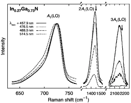
B. Near-resonance behavior and multiphonon scattering
As discussed in Sec. IIA, resonant effects give rise to the intensity enhancement displayed by the polarA1共LO兲mode in the mid- to low-In composition alloys 共0.16艋x艋0.37兲. Beside the enhancement of the Raman intensity of the infrared-active modes, electron–phonon coupling via the Fröhlich interaction can produce, near resonance, very strong scattering by 2LO phonons and higher-order multiphonon scattering.26For excitation above the band gap in the absorp-tion continuum, resonant multiphonon Raman-scattering lines were observed in the photoluminescence of doped GaN
共Ref. 27兲and resonant Raman scattering byn-LO modes up ton= 7 were reported for Be- and C-implanted GaN.28
in the spectrum excited with the 2.41-eV line was about 40 times higher than in the spectrum excited with the 2.71-eV line.
The A1共LO兲 peak shifts to lower frequencies by about 4 cm−1 and broadens asymmetrically towards low frequen-cies when the excitation energy is reduced from 2.71 to 2.41 eV. This behavior cannot be explained by strain gradients along the growth direction reported in InGaN al-loys, because the longer excitation wavelengths are less ab-sorbed and therefore, probe a deeper region where the sample is more strained.22 This effect would lead to high-frequency shifts of the phonons excited with the 2.41-eV line, contrary to the experimental observation. On the other hand, frequency shifts in the A1共LO兲 Raman peak can be attributed to selective resonant excitation of regions with dif-ferent In contents.2,3 For lower excitation energies, regions with higher In fraction will have a matching band gap. Ac-cording to Ref. 23, an In fraction of x= 0.27 yields a band gap of 2.42 eV, whereasEG= 2.71 occurs atx= 0.19. Higher In composition yields lower phonon frequencies, which is consistent with the observed downshift of theA1共LO兲mode in the spectra excited with the 2.41-eV line. However, the magnitude of the observed downward shift 共⬇4 cm−1兲 is smaller than the shift expected for an increase of In fraction from x= 0.19 to x= 0.27, which according to Ref. 10 is
⬇13 cm−1. This suggests that the selective resonance shift is partly compensated by the strain gradient effect discussed above.
We note that a substantialA1共LO兲 asymmetrical broad-ening is observed for the lower excitation energies; the full width at half height increases from 33 cm−1at 2.71 eV up to 62 cm−1 at 2.41 eV. Such a broadening cannot be attributed to disorder in the deeper region probed by the 2.41-eV exci-tation, since it was shown that the density of structural de-fects is higher in the upper part of the InxGa1−xN films.
22
This broadening actually reflects the distribution of regions with different In fractions in the scattering volume, and
therefore the asymmetric line shape of theA1共LO兲mode can-not be accounted for solely in terms of phonon correlation length, as suggested in previous works.8
The Raman spectrum excited with the 2.41-eV line dis-plays a weak 2LO peak, but no signal in the 3LO region could be detected. The relative intensity of the 2LO peak increases substantially under excitation with the 2.54-eV line and a 3LO feature begins to be visible. By increasing the excitation energy to 2.60 eV, which as mentioned above is close to the 2LO outgoing resonance in this sample, 2LO scattering becomes as intense as first-order scattering. A strong enhancement of 2LO scattering near the outgoing resonance is characteristic of an iteration of the intraband Fröhlich interaction via excitonic intermediate states.29 Two-LO-phonon scattering is mainly governed by near zone-center phonons because of the q−1 dependence of the Fröhlich interaction. Thus, it gives rise to sharp peaks at about twice the frequency of the first-order LO peak. We observe a 2LO peak which is centered about 10 cm−1below the exact multiple of the first-order frequency 共arrow兲 and exhibits a slight asymmetry with a low-frequency tail. Both features could result from the combined effect of the partici-pation of q⫽0 phonons and the distribution of different In fractions in the film. Even though the 3LO intensity is higher with the 2.60-eV excitation than with the 2.54-eV excitation, the 3LO/2LO intensity ratio is roughly the same. By contrast, excitation with the 2.71-eV line greatly enhances the 3LO peak, which becomes comparable in intensity with the 2LO peak. The 2.71-eV line is close to the outgoing 3LO reso-nance. Then, resonant Raman scattering via real intermediate exciton states in a cascade process30 becomes possible, which contributes to the strong intensity observed for the 3LO peak. Since wave-vector conservation in the cascade model requires the emission ofq⫽0 LO phonons, the 3LO Raman peak contains important contributions from phonons away from the zone center. This is reflected in a peak fre-quency clearly below 3LO共⌫兲, as can be seen in Fig. 3. No Raman signal was detected in the 4LO frequency region due to the small probability of high-order scattering and the ex-citation energy being too low to excite a cascade process involving four LO phonons.
IV. CONCLUSION
We have carried out a Raman-scattering study of the phonon behavior of the InxGa1−xN alloy over the whole com-position range. The one-mode behavior of theA1共LO兲andE2 modes has been confirmed and the respective phonon fre-quencies have been determined for the whole composition range, showing good agreement with the previous MREI model calculations. We have found systematic frequency de-viations in MBE-grown samples that we ascribe to local structural differences in bond length also detected by EXAFS measurements. A substantial broadening is observed for in-termediate In fractions due to intrinsic disorder and compo-sition fluctuations.
[image:4.612.64.283.47.220.2]In most samples, theA1共LO兲mode displays a very high intensity relative to theE2mode, which indicates a resonant enhancement via Fröhlich mechanisms of the polar A1共LO兲
mode. A more detailed study using above band-gap excita-tion for the sample withx= 0.27 revealed a frequency shift of the A1共LO兲 mode with excitation wavelength that can be accounted for by the selective excitation of regions with dif-ferent In contents. This effect has been shown to be partly compensated by the presence of strain gradients along the growth direction. Excitation in near outgoing resonance con-ditions allowed us to observe strong multiphonon peaks up to 3LO.
ACKNOWLEDGMENTS
This work has been supported by the Spanish Ministry of Science and Technology under Contract No. MAT2001-1878. One of the authors共S.H.兲acknowledges financial sup-port from the Spanish Ministry of Education and Science.
1S. Nakamura, M. Senoh, N. Iwasa, S. Nagahama, T. Yamada, and T.
Mu-kail, Jpn. J. Appl. Phys., Part 2 34, L1332共1995兲.
2D. Behr, J. Wagner, A. Ramakrishnan, H. Obloh, and K.-H. Bachem,
Appl. Phys. Lett. 73, 241共1998兲.
3N. Wieser, O. Ambacher, H.-P. Felsl, L. Görgens, and M. Stutzmann,
Appl. Phys. Lett. 74, 3981共1999兲.
4S. Pereira, M. R. Correira, E. Pereira, K. P. O’Donnell, C. Trager-Cowan,
F. Sweeney, and E. Alves, Phys. Rev. B 64, 205311共2001兲.
5M. R. Correia, S. Pereira, E. Pereira, J. Frandon, and E. Alves, Appl. Phys.
Lett. 83, 4761共2003兲.
6L. Artús, R. A. Stradling, Y. B. Li, S. J. Webb, W. T. Yuen, S. J. Chung,
and R. Cuscó, Phys. Rev. B 54, 16373共1996兲.
7S. Hernández, N. Blanco, I. Mártil, G. González-Díaz, R. Cuscó, and L.
Artús, J. Appl. Phys. 93, 9019共2003兲.
8T. Sugiura, Y. Kawaguchi, T. Tsukamoto, H. Andoh, M. Yamaguchi, K.
Hiramatsu, and N. Sawaki, Jpn. J. Appl. Phys., Part 1 40, 5955共2001兲. 9D. Alexsonet al., J. Appl. Phys. 89, 798共2001兲.
10H. Grille, C. Schnittler, and F. Bechstedt, Phys. Rev. B 61, 6091共2000兲. 11C. J. Deatcher, C. Liu, S. Pereira, M. Lada, A. G. Cullis, Y. J. Sun, O.
Brandt, and I. M. Watson, Semicond. Sci. Technol. 18, 212共2003兲. 12F. B. Naranjo, S. Fernández, M. A. Sánchez-García, F. Calle, E. Calleja,
A. Trampert, and K. H. Ploog, Mater. Sci. Eng., B 93, 131共2002兲. 13M. Kurouchi, T. Araki, H. Naoi, T. Yamaguchi, A. Suzuki, and Y. Nanishi,
Phys. Status Solidi B 241, 2843共2004兲.
14R. W. Martin, P. R. Edwards, K. P. O’Donnell, E. G. Mackay, and I. M.
Watson, Phys. Status Solidi A 192, 117共2002兲. 15S. Pereiraet al., Appl. Phys. Lett. 81, 1207共2002兲. 16J. W. Trainor and K. Rose, J. Electron. Mater. 3, 821共1974兲.
17L. Siozade, J. Leymarie, P. Disseix, A. Vasson, M. Mihailovic, N.
Grand-jean, M. Leroux, and J. Massies, Solid State Commun. 115, 575共2000兲. 18S. Yu, K. W. Kim, L. Bergman, M. Dutta, M. A. Stroscio, and J. M.
Zavada, Phys. Rev. B 58, 15283共1998兲.
19V. Y. Davydovet al., Appl. Phys. Lett. 75, 3297共1999兲.
20G. Abstreiter, M. Cardona, and A. Pinczuk,Light Scattering in Solids IV, Topics in Applied Physics Vol. 54共Springer, Berlin, 1984兲.
21L. Artús, R. Cuscó, J. Ibáñez, N. Blanco, and G. González-Díaz, Phys.
Rev. B 60, 5456共1999兲.
22M. R. Correiaet al., Appl. Phys. Lett. 85, 2235共2004兲.
23J. Wu, W. Walukiewicz, K. M. Yu, J. W. Agen III, E. E. Haller, H. Lu, and
W. J. Schaff, Appl. Phys. Lett. 80, 4741共2002兲. 24V. Y. Davydovet al., Phys. Rev. B 58, 12899共1998兲.
25V. Katchkanovet al., Mater. Res. Soc. Symp. Proc. 831, E3.30共2004兲. 26M. Cardona,Light Scattering in Solids II, Topics in Applied Physics Vol.
50共Springer, Berlin, 1982兲.
27D. J. Dewsnipet al., Semicond. Sci. Technol. 12, 55共1997兲.
28W. H. Sun, S. J. Chua, L. S. Wang, and X. H. Zhang, J. Appl. Phys. 91,
4917共2002兲.
29A. García-Cristóbal, A. Cantarero, C. Trallero-Giner, and M. Cardona,
Phys. Rev. B 49, 13430共1994兲.