Schirmer, S G and Oi, D K L and Greentree, A D (2005) Controlled phase
gate for solid-state charge-qubit architectures. Physical Review A, 71 (1).
-. ISSN 1094-1622 , http://dx.doi.org/10.1103/PhysRevA.71.012325
This version is available at
https://strathprints.strath.ac.uk/35335/
Strathprints is designed to allow users to access the research output of the University of Strathclyde. Unless otherwise explicitly stated on the manuscript, Copyright © and Moral Rights for the papers on this site are retained by the individual authors and/or other copyright owners. Please check the manuscript for details of any other licences that may have been applied. You may not engage in further distribution of the material for any profitmaking activities or any commercial gain. You may freely distribute both the url (https://strathprints.strath.ac.uk/) and the content of this paper for research or private study, educational, or not-for-profit purposes without prior permission or charge.
Any correspondence concerning this service should be sent to the Strathprints administrator:
The Strathprints institutional repository (https://strathprints.strath.ac.uk) is a digital archive of University of Strathclyde research outputs. It has been developed to disseminate open access research outputs, expose data about those outputs, and enable the
arXiv:quant-ph/0410062v1 8 Oct 2004
S. G. Schirmer,1, 2,∗ D. K. L. Oi,1 and Andrew D. Greentree3 1
Department of Applied Mathematics and Theoretical Physics, University of Cambridge, Wilberforce Road, Cambridge CB3 0WA, UK 2
Department of Engineering, University of Cambridge, Trumpington Street, Cambridge, CB2 1PZ, UK 3
Centre for Quantum Computer Technology, School of Physics, University of Melbourne, Melbourne, Victoria 3010, Australia
(Dated: February 1, 2008)
We describe a mechanism for realizing a controlled phase gate for solid-state charge qubits. By augmenting the positionally defined qubit with an auxiliary state, and changing the charge distri-bution in the three-dot system, we are able to effectively switch the Coulombic interaction, effecting an entangling gate. We consider two architectures, and numerically investigate their robustness to gate noise.
PACS numbers: 03.67.Lx,03.65.Vf,85.35.Be
I. INTRODUCTION
The search for a workable quantum information pro-cessor is an effort that has captivated the attention of researchers in many disciplines. A quantum computer re-quires individual quantum logic elements, usually qubits, and entangling interactions between these elements [1, 2]. Solid-state proposals are widely seen as being some of the most attractive from the point of view of con-structional scalability, i.e., the ability to replicate many qubits. Furthermore, schemes compatible with present semiconductor technologies [3, 4, 5, 6] are especially at-tractive because of their potential to leverage the associ-ated industrial experience [7, 8].
In this paper we concentrate on charge-based archi-tectures. Such systems were amongst the first pro-posed for quantum computing [9] and numerous versions have evolved recently [6, 10, 11, 12]. We are attracted to charge-based systems for three reasons: (1) proven high-fidelity readout compatible with single-shot opera-tions [13]; (2) potential for high-speed (∼picosecond) op-erations [6]; and (3) the ability to define variable dimen-sionality Hilbert spaces by appropriate partitioning [14]. The usual mechanism for coupling charge qubits is via the Coulomb interaction. In general, this interaction cannot be controlled without a variation in the charge distribu-tion in the qubits. In this paper we specifically address this issue and show how to make a scalable controlled phase gate that makes use of the Coulomb interaction.
The Coulomb interaction is insensitive to minor vari-ations in the distance between the quantum dots and its strength lends itself to high-speed entangling oper-ations; conversely, its long-range nature makes it diffi-cult to effectively modulate interactions between qubits. Most charge qubit schemes so far proposed implicitly rely on a fixed, always-on Coulomb interaction between qubits [6, 10, 15] Such schemes would necessarily require
∗Electronic address: [email protected]
global control techniques [16, 17, 18], which may be prob-lematic given the strength of the Coulomb interaction.
In the following we first discuss local qubit operations (Sec. II) and introduce the two-qubit interaction Hamil-tonian (Sec. III). Then we describe how to realize a con-trolled phase gate and analyze its operation in terms of dynamic and geometric phases (Sec. IV). Finally, we discuss various practical issues such as the detrimental effects of finite rise and decay times on the gate fidelity and how to correct them (Sec. V), gate implementation in the presence of practical constraints on pulse lengths and tunnelling rates (Sec. VI), and the effect of noisy controls (Sec. VII) and imperfect architectures (Sec. VIII) on the gate performance.
II. SINGLE QUBIT SYSTEM
As will be shown below, a three-dot system is required to modulate the Coulomb interaction. We therefore sup-plement the canonical charge qubit with an auxiliary state and define a quantum element with three quantum dots and one charge, where the position of the charge on two sites defines the qubit and the third site defines an auxiliary state used for two-qubit interactions. We work only with the ground state of each dot. We further as-sume that the ground states are energetically close and sufficiently separated from higher-lying excited states, so that the excitation of these states can be neglected. The system can thus be approximated as a three level system with Hamiltonian
ˆ
H =
3
X
d=1
ǫd|dihd|+~
X
d′6=d
µdd′Xˆdd′, (1)
where|didenotes the ground state of the electron local-ized in dotdford= 1,2,3,ǫdthe energy of state|di,µdd′
the tunnelling rate between dotsd and d′ (for d′ 6=d),
and ˆXdd′=|dihd′|+|d′ihd|. We shall assume that we can
qubit
auxiliary
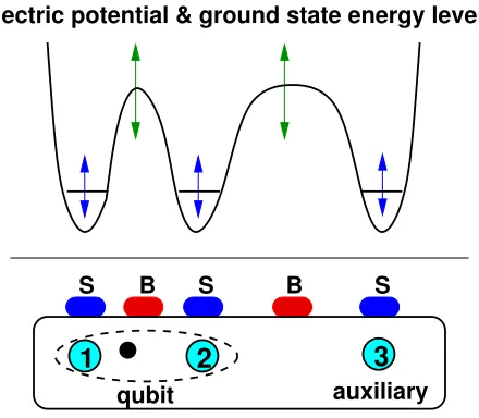
electric potential & ground state energy levels
S
B
S
B
S
[image:3.612.71.291.51.243.2]1
2
3
FIG. 1: Schematic of a single qubit-plus-auxiliary unit (bot-tom) and electronic potential (top). The large circles
repre-sent the quantum dots, the black dot the shared electron. S
andBsurface electrodes serve to shift the ground state energy
of the dots and change the height of the tunnelling barriers and thus the tunnelling rates between them.
ratesµdd′, e.g., by varying the voltages applied to several
control electrodes as illustrated in Fig. 1.
To implement local unitary operations, we inhibit tun-nelling to the auxiliary site by raising the barrier be-tween dots 2 and 3 (and/or 1 and 3 if applicable), or increasing the ground state energy of the auxiliary dot 3. In practice, the precise functional dependence of ǫd andµdd′ on the control voltages applied should be
deter-mined experimentally using Hamiltonian identification techniques [19]. When µ13=µ23= 0 the local
Hamilto-nian can be rewritten as
ˆ
H =ǫ1|1ih1|+ǫ2|2ih2|+~µ12Xˆ12+ǫ3|3ih3|, (2)
and we can realize arbitrary unitary operations on the qubit subspace by changing the energy levelsǫd and the tunnelling rateµ12. For instance, shifting the energy level
of dot 2 by ǫ2(t) for t0 ≤t≤t1 results in a local phase
rotation
ˆ
U2(φ) =|1ih1|+e−iφ|2ih2|+|3ih3|, (3)
withφ=Rt1
t0 ǫ2(t)/
~dt. Effecting a tunnelling rate ofµ12 fort0≤t≤t1gives
ˆ
U12(α) = cos(α) ˆI12−isin(α) ˆX12+|3ih3|, (4)
where the rotation angle isα=Rt1
t0 µ
(k)
12(t)dt and ˆI12 =
|1ih1|+|2ih2|. By combining two phase rotations on the 2nd dot with a tunnelling gate between sites 1 and 2, for example, we can implement any local unitary operation on the qubit subspace modulo global phases [2]
ˆ
U(φ1, α, φ2) = ˆU2(φ2) ˆU12(α) ˆU2(φ1),
=
cos(α) −ie−iφ1sin(α) 0
−ie−iφ2sin(α) e−i(φ1+φ2)cos(α) 0
0 0 1
,
(5)
For example, a Hadamard transform on the qubit sub-space corresponds to
ˆ
H= √1 2
1 1
1 −1
!
= ˆUφ2=− π
2, α=
π
4, φ1=−
π
2
.
(6) It is possible to optimize the implementation of some lo-cal unitary operations by simultaneously changing mul-tiple control parameters. See appendix A.
III. INTERACTION HAMILTONIAN
To achieve entangling operations it is necessary to change the charge distribution of adjacent elements. Al-though almost any interaction will lead to entangle-ment [20], the resulting dynamics may be neither easy to utilize, nor robust against noise.
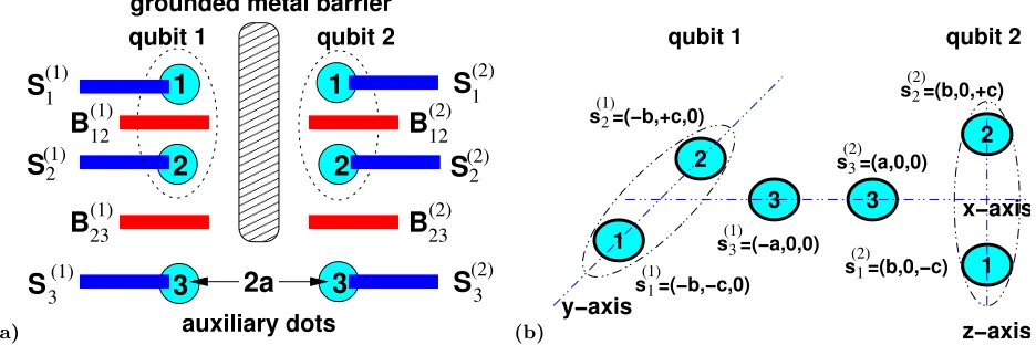
Rather than choose an arbitrary interaction, it is more useful to consider geometries where the action of the Coulomb force on the qubit states is trivial. One way this might be achieved is by using shielding to eliminate direct interactions between qubits but not between the auxiliary sites as shown in Fig. 2 (a). Such a system could be fabricated in a GaAs 2DEG system [11, 21] or a pil-lar system [22], for instance. An alternative is to choose a geometry for which the effect of the Coulomb inter-action on the dynamics of the qubit subspace is trivial, resulting only in a global phase factor, as in Fig. 2 (b). To fabricate such a structure, we would propose an ex-tension of the atomic placement techniques used for Si:P systems [23, 24]. Both designs have the advantage of al-lowing the implementation of controlled two-qubit gates using simple pulse sequences. Note that using auxiliary sites has also been proposed as a way to allow generalized readout of quantum information in different bases [25].
The Hilbert space for two qubit-plus-auxiliary units is spanned by the states |dd′i for d, d′ = 1,2,3, where
|dik denotes the dth basis state for the kth unit, and |dd′i=|di
1⊗|d′i2are the tensor product states as usual.
The total Hamiltonian of this system is
ˆ
H = ˆH(1)⊗Iˆ
3+ ˆI3⊗Hˆ(2)+ ˆHC, (7)
where ˆI3 is the identity matrix in dimension three, ˆH(k)
for k = 1,2 is the local Hamiltonian for the kth qubit-plus-auxiliary unit specified in Eq. (1), and ˆHC is the Coulomb Hamiltonian
ˆ
HC= 3
X
d,d′=1
(a) (1) 1
S
12 (1)B
(1) 2S
23 (1)B
(1)S
3S
(2)323 (2)
B
(2) 2S
12 (2)B
(2) 1S
3
2
000 000 000 000 000 000 000 000 000 000 000 000 000 000 111 111 111 111 111 111 111 111 111 111 111 111 111 1112a
3
2
1
1
grounded metal barrier
auxiliary dots
qubit 1
qubit 2
(b) 1 2 3 3 1 2 3 (1) s =(−a,0,0) 1 (2) s =(b,0,−c) 3 (2) =(a,0,0) s 2 (2) s =(b,0,+c) 2 (1) =(−b,+c,0) s 1 (1) =(−b,−c,0) s z−axis x−axis qubit 2 y−axis qubit 1
FIG. 2: (a) Two-qubit system with two auxiliary sites comprised of six quantum dots (filled circles). A grounded metal barrier shields the Coulomb interaction between nearby quantum dots except between the two auxiliary sites (3). The thick (red and
blue) lines indicate the surface control electrodesBdd(k)′ andS
(k)
d , respectively. (b) 3D geometry for a two-qubit system with
auxiliary sites, for which the Coulomb interaction between the two charges is constant if both are confined to their respective qubit subspace comprised of dots 1 and 2, but differs from the Coulomb coupling between the auxiliary dots provided that
√
4b2+ 2c2 6= 2a. Note that the inter-dot distances satisfy ks(1)
d −s
(2)
d′ k =
√
4b2+ 2c2 and ks(1) 3 −s
(2)
d k = ks
(1)
d −s
(2) 3 k =
p
(a+b)2+c2 ford, d′= 1,2.
The Coulomb interaction energiesγdd′ are given by
γdd′ =
e2
4πǫks (1) d −s
(2) d′ k−
1, (9)
where s(k)
d denotes the position of thedth quantum dot in the kth qubit-plus-auxiliary unit, ǫ is the applicable dielectric constant, ande is the electron charge. In pure silicon we haveǫ= 11.8ǫ0, whereǫ0is the dielectric
con-stant in vacuum. If two sitess(1)
d ands (2)
d′ are separated by a sufficiently
thick, grounded metal barrier thenγdd′ = 0. Hence, the
Coulomb interactions for the shielded 2D geometry in Fig. 2 (a) effectively vanish except forγ33. Similarly, for
the 3D geometry shown in Fig. 2 (b), symmetry implies
γ11=γ12=γ21=γ22 ≡ γ1, γ13=γ23=γ31=γ32 ≡ γ2.
We can cancel the effect of the Coulomb interaction be-tween qubit states by applying suitable bias voltages to the energy shift gates to offset the energy levelsǫ(1k) and ǫ2(k) by −γ1/2 and ǫ3(k) byγ1/2−γ2 for k= 1,2. Thus,
the Coulomb interaction Hamiltonian becomes
ˆ
HC=γeff|33ih33|, (10)
whereγeff is the effective Coulomb coupling between the
auxiliary states, i.e., ˆHC acts trivially on the system ex-cept if both electrons are in the auxiliary states.
For a 2D architecture with shielding γeff will usually
be less than the free-space Coulomb interaction γ33 due
to screening and image charges. For a 3D geometry with energy offsetsγeff will be less than or equal toγ33−2γ2+ γ1, with equality if the screening due to control electrodes
etc. is negligible.
For convenience, we choose the effective Coulomb en-ergyγeff between the auxiliary sites as the unit of energy
such that the free evolution Hamiltonian of the two-qubit plus auxiliary system is ˆH0 = |33ih33|. All tunnelling
rates are given in units ofγeff/~ and the canonical time
unit is~/γeff.
IV. CONTROLLED TWO-QUBIT PHASE GATE
To motivate the design of a two-qubit phase gate, we note that the phase acquired by an electron tunnelling be-tween two quantum dots depends on the energy difference between them. In our system the energy differences are determined by a combination of energy bias voltages and the Coulombic interaction between the auxiliary sites. Hence, by adjusting the voltage on the energy bias gate
S2(1), for instance, we can shift of the energy of state|2i1
such that the energy differences between states|21iand |31i, and|23iand|33i, respectively, are equal in magni-tude but opposite in sign, as illustrated in Fig. 3. In this case the phase acquired by a charge tunnelling between dots 2 and 3 of qubit 1 will have the same magnitude regardless of the population of state|3i2, but the latter
will determine its sign. This observation is central to the operation of our controlled phase gate.
To achieve a maximally entangling gate, the acquired phases in both cases must differ by an integer multiple of
π. Finally, except for the acquired phase, the charge must return to its initial state|2i1 at the end of the tunnelling
[image:4.612.76.544.56.212.2]23
21
33
31
[image:5.612.56.296.52.197.2]∆ε = −1/2
∆ε = +1/2
FIG. 3: Energy level configuration during the second step:
By applying an energy bias ofǫ(1)2 = 1/2 we ensure that the
energy gap between states|23iand|33i, and|21iand|31iis
±1/2, respectively.
the following expressions for the tunnelling rate
µ(1)23 =
1 4
s
2n
2k−1
2
−1, (11)
for suitable positive integers n and k satisfying 2n >
2k−1, and tunnelling time
τ2=
4πn r
16µ(1)23
2
+ 1
= 2π(2k−1). (12)
A detailed explanation of these results is provided in ap-pendices C and D. Furthermore, the phase acquired by state|21iis [2n−(2k−1)]π/2, while that of state |23i is [2n+ (2k−1)]π/2, and hence the phase difference is (2k−1)π≡πas desired.
In the absence of constraints on the tunnelling rates and pulse lengths, the gate operation time is optimized if we choosen=k= 1 andµ(1)23 =
√
3/4. For details about how to choosenandkwhen there are constraints on the tunnelling rates and pulse lengths, see appendix E.
More explicitly, a maximally entangling controlled two-qubit phase gate
ˆ
Uphase = |11ih11|+|12ih12|+|21ih21| − |22ih22|
= diag( ˆI2,Zˆ12). (13)
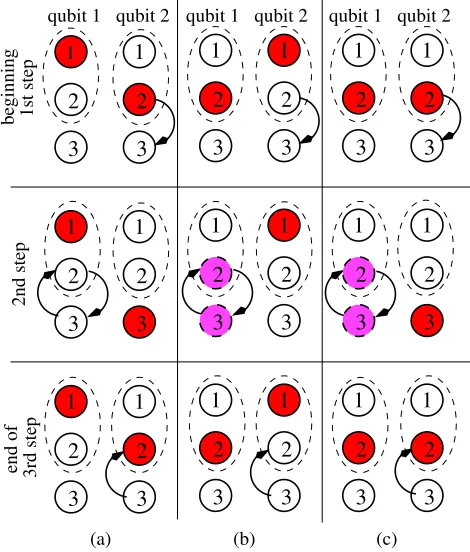
can be realized as follows:
1. Acting on thesecond qubit, swap the populations of the states|2i2and|3i2by lowering the tunnelling
barrier between the 2nd and 3rd quantum dot for time τ1 = π/(2µ(2)23), where µ
(2)
23 is the tunnelling
rate.
2. Acting on thefirst qubit, simultaneously raise the ground state energy of the 2nd dot by ǫ(1)2 = 1/2
and lower the tunnelling barrier between the 2nd and 3rd dot to achieve the tunnelling rate given by Eq. (11) for the time specified by Eq (12).
1
3
3
1
2
3
2
3
1
3
2
qubit 1 qubit 2
1
3
1
1
2
1
3
1
3
1
3
qubit 2 qubit 1
2
2
2
3
2
2
3
3
3
2
3
3
1
1
1
2
2
2
3
1
1
2
3
2
1
beginning 1st step
2nd step
end of 3rd step
(a) (b) (c)
qubit 1 qubit 2
1
1
1
2
2
2
3
FIG. 4: Schematic representation of the phase gate operation for three initial basis states (a) |12i, (b)|21i, and (c) |22i.
The operation for|11ihas been omitted because it is trivial.
The filled (red) dots show the positions of the electrons at the beginning of the first step (top), during the second step (middle), and after completion of the third step (bottom). For initial configurations|21i(b) and|22i(c), the first charge is in
a superposition of states|2i1 and|3i1during the second step,
and hence acquires a phase conditional on the population of
state |3i2, which is indicated by by lighter (pink) shading.
Notice, however, that the electron starts and ends in state
|2i1, except for the conditional phase acquired.
3. Acting on thesecond qubit, repeat the first step to swap the populations of states|2i2and|3i2 back.
4. Acting simultaneously on both qubits, shift the en-ergy of states |2i1 and |2i2 by ǫ(1)2 = ℓπ/τ4 and ǫ(2)2 =π/τ4, respectively, for some time τ4, where ℓ= 1/2−(n+k) mod 2. (See appendix D.)
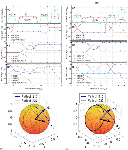
The first three steps are illustrated in Fig. 4, and Fig. 5 shows results for a simulation of the gate for ideal pulses and no constraints.
Since this gate combined with local unitary operations as described in Sec. II is universal, we can implement any desired two-qubit gate. For instance, a controlled-NOT gate is performed simply by applying a Hadamard transformation on the second qubit before and after the pulse sequence above.
Further analysis shows that the conditional phase ac-quired by state|2i1 is exactly twice the geometric phase
[image:5.612.320.555.56.332.2]−1 −0.5 0 0.5 1
Ψ
(t) for
Ψ
(0) = |12
〉
pop. of |12〉 pop. of |13〉 angle[〈Ψ(0),Ψ(t)〉]/π
−1 −0.5 0 0.5 1
Ψ
(t) for
Ψ
(0) = |21
〉
|〈 21|21〉|2 |〈 31|31〉|2 angle[〈Ψ(0),Ψ(t)〉]/π
0 2 4 6 8 10 12 14 16
−1 −0.5 0 0.5 1
time [units of h/(2πγeff)]
Ψ
(t) for
Ψ
(0) = |22
〉
|〈 22|22〉|2 |〈 23|23〉|2 |〈 33|33〉|2 angle[〈Ψ(0),Ψ(t)〉]/π 0
0.5 1
Controls [units of
γeff
]
hµ23(2)/(2π) hµ23(2)/(2π)
hµ 23
(1)/(2π)
ε2(1)
ε2(1) ε
2 (2) (a)
[image:6.612.57.294.51.372.2](d) (c) (b)
FIG. 5: Operation of the proposed controlled phase gate for ideal controls with no constraints. Shown are the control pa-rameter settings (a) and the corresponding evolution of the initial states (b)|12i, (c)|21iand (d)|22i. The evolution of
|11i, being trivial, has been omitted. In each case, only the
relevant populations and acquired phases are plotted.
andS2={|23i,|33i}, respectively. To see this, note that
the Hamiltonians forS1andS2 are
ˆ
HS1 =
1
4Iˆ2+µσˆx+ 1
4ˆσz (14)
ˆ
HS2 =
3
4Iˆ2+µσˆx− 1
4ˆσz (15)
withµ= (p
(2n)2/(2k−1)2−1)/4, and we can visualize
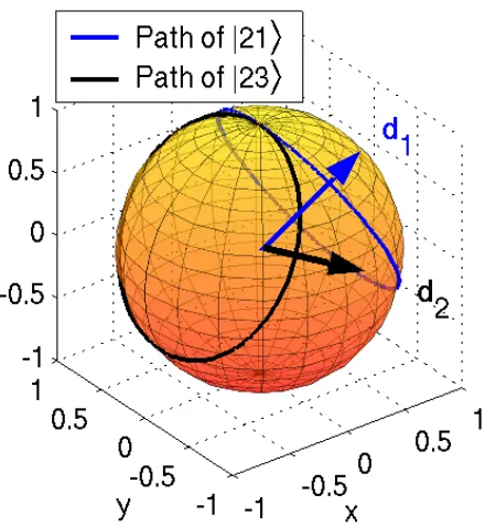
their evolution on the Bloch sphere as in Fig. 6. Let
s= (sx, sy, sz) withsα= Tr(σαρ) forα∈ {x, y, z}be the
usual Bloch vector. The initial states |21i and |23i for
S1 andS2, respectively, correspond to the Bloch vector s0 = (0,0,1), and their evolution in R3 to a rotation about the axesd1= 2(µ,0,1/4) andd2 = 2(µ,0,−1/4),
respectively.
The pure-state non-adiabatic, cyclic geometric phase [26] isφgeom= Ω2 = 2πn(1−cosθ), where Ω is the
solid angle subtended by the Bloch vector,nis the num-ber of times the Bloch vector rotates around the axisd,
andθis the angle between the initial state vectors0 and
[image:6.612.315.535.61.300.2]the rotation axis d. Both states rotate with the same
FIG. 6: Trajectory of the Bloch vectors associated with the
two-level subsystems S1 and S2 for ideal phase gate. For
n= k = 1 the Bloch vectors s1(t) (cyan) and s2(t) (black)
rotate aboutd1andd2, respectively, simultaneously
complet-ing a scomplet-ingle closed loop on the surface of the Bloch sphere and
sweeping out solid angles ofπ (area “inside” the blue loop)
and 3π(area “outside” the black loop), respectively. Hence,
the difference between the areas is 2π, and the conditional
phase acquired by state|2i1 depending on whether state|3i2
is occupied will differ byπ.
frequency kdk = kd′k = (p
1 + 16µ2)/2 = n/(2k−1),
and hence the relative geometric phase depends on θ. Noting that
cos(θ1) =
d1·s0
kd1k =
2k−1
2n =−cos(θ2), (16)
we see that the respective geometric phases acquired by
S1andS2 are 2πn[1−(2k−1)/(2n)] =π[2n−(2k−1)]
and 2πn[1+(2k−1)/(2n)] =π[2n+(2k−1)], i.e., exactly twice the conditional phases acquired by states|21iand |23i.
V. REALISTIC CONTROLS AND
CORRECTION OF SYSTEMATIC ERRORS
0 0.51
A
[image:7.612.57.292.51.183.2]0
τ
sτ
−
τ
sτ
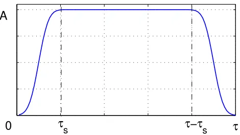
FIG. 7: Realistic square-wave pulse of amplitudeAand length
τ with rise and decay timeτs, modelled using error functions.
τs 0.25 0.50 0.75 1.00 1.25 1.50
Eu 0.0223 0.0825 0.1691 0.2659 0.3559 0.4251
Ec×104 0.2225 0.2249 0.2273 0.2294 0.2311 0.2325
TABLE I: Gate error E = 1− F as a function of the pulse
rise and decay time τs for non-ideal, uncorrected (Eu) and
corrected pulses (Ec) for simulations with time step ∆t =
0.005.
for pulse rise and decay times ofτs= 1 time unit. Com-paring the trajectories shows that there are significant population and phase errors. In particular, the popula-tions of the states|13i,|31iand|33ido not return to 0, i.e., population is lost to the auxiliary states, a poten-tially difficult error to correct.
To quantitatively compare the gates implemented to the ideal gate we consider theaverage gate fidelity[27, 28]
F =hΨin|Uˆ†ρˆoutUˆ|Ψini, (17)
which is a measure of the overlap of the final state ˆρout
with the desired target state ˆU|Ψiniaveraged over all
in-put states. Since ˆρout may extend to the auxiliary
quan-tum dots, the fidelity includes the effect of population losses to these states.
In the example shown in Fig. 8 pulse rise and decay times of one time unit reduce the average gate fidelity from one in the ideal case to∼73 %. Table I shows that even relatively small rise and decay times of the fields tend to reduce the average gate fidelity noticeably. This increase in the gate error appears to be mainly due to population loss to the auxiliary states.
The first step toward improving the results is to re-alize that rise and decay times reduce the total pulse area. An ideal square-wave pulse (τs= 0) of durationτ with amplitude A has a pulse area ofAτ, while that of a similar pulse with rise and decay timeτs< τ /2 is only
A(τ−τs) [29]. Since the pulse area is an important con-trol parameter, we must therefore adjust either the field strengths or the pulse lengths, or possibly both. For the 1st, 3rd and 4th step of the CPHASE gate correcting the
pulse area is all that is needed to eliminate systematic er-rors due to non-zero pulse rise and decay times, and we can achieve this either by increasing the field strength or the pulse durations.
During the crucial 2nd step, the energy of state |2i1
should be kept constant ǫ(1)2 = 1/2 while tunnelling is enabled, and the value of the tunnelling rateµ(1)23 should
be close to one of the desired values. Increasing the field strengths to compensate for rise and decay times is thus not an option for this step. For simplicity, we shall there-fore correct the pulse areas by increasing the duration of each pulse byτs, i.e., setting τk′ = τk +τs, where τk is the duration of the corresponding ideal pulse.
To improve the accuracy of the 2nd step further, we raise the energyǫ(1)2 at leastτs time units before we en-able tunnelling between states |2i1 and |3i1, and lower
it only after the tunnelling barrier has been raised again to inhibit tunnelling. Since changing the energy of state |2i1 is a local operation on the first qubit, it commutes
with the swap operation on states|2i2 and|3i2. We can
therefore begin to raise the energy of state |2i1 before
the 1st swap operation is completed, and we can begin the 3rd swap operation before ǫ(1)2 (t) has reached zero. However, the increased duration of the energy shift will induce an additional local phase shift, which has to be taken into account in the final step to achieve the desired gate. Lett1=τ1′−τsandt2=τ1′+τ2′+τs and
∆φ=
Z t2
t1
ǫ(1)2 (t)dt−
1
2τ2, (18)
whereτ2is the time required to complete the second swap
operation for ideal, piecewise constant control pulses. Then the local phase rotation on the first qubit required in the final step is Φ = ℓπ−∆φ instead of ℓπ, where
ℓ= 12−(n+k) mod 2 as before. Thus, in the final step the energy of state|2i1 must be raised by
ǫ(1)2 =
πℓ−∆φ
τ4 (19)
whereτ4 is the duration of the step for ideal, piecewise
constant controls.
Numerical simulations indicate that these corrections greatly enhance the performance of the phase gate. For instance, Table I shows that the average gate error Ec with these corrections is less than 10−4 for all rise and
decay timesτs[33] and Fig. 8 (II) shows that the trajec-tories very closely match those of the ideal gate.
VI. GATE OPERATION TIMES AND
PHYSICAL CONSTRAINTS
(I) (II)
−1 −0.5 0 0.5 1
Ψ
(t) for
Ψ
(0) = |12
〉
pop. of |12〉 pop. of |13〉 angle[〈Ψ(0),Ψ(t)〉]/π
−1 −0.5 0 0.5 1
Ψ
(t) for
Ψ
(0) = |21
〉
|〈 21|21〉|2 |〈 31|31〉|2 angle[〈Ψ(0),Ψ(t)〉]/π
0 2 4 6 8 10 12 14 16
−1 −0.5 0 0.5 1
time [units of h/(2πγeff)]
Ψ
(t) for
Ψ
(0) = |22
〉
|〈 22|22〉|2 |〈 23|23〉|2 |〈 33|33〉|2 angle[〈Ψ(0),Ψ(t)〉]/π 0
0.5 1
Controls [units of
γeff
]
hµ23(2)/(2π) hµ23(2)/(2π)
hµ 23
(1)/(2π)
ε2(1)
ε2(1) ε2(2) (a)
(b)
(c)
(d)
0 0.5 1 1.5
Controls [units of
γeff
]
−1 −0.5 0 0.5 1
Ψ
(t) for
Ψ
(0) = |12
〉
pop. of |12〉 pop. of |13〉 angle[〈Ψ(0),Ψ(t)〉]/π
−1 −0.5 0 0.5 1
Ψ
(t) for
Ψ
(0) = |21
〉
|〈 21|21〉|2 |〈 31|31〉|2 angle[〈Ψ(0),Ψ(t)〉]/π
0 2 4 6 8 10 12 14 16 18
−1 −0.5 0 0.5 1
time [units of h/(2πγeff)]
Ψ
(t) for
Ψ
(0) = |22
〉
|〈 22|22〉|2 |〈 23|23〉|2 |〈 33|33〉|2 angle[〈Ψ(0),Ψ(t)〉]/π
hµ23(2)/(2π) hµ
23 (2)/(2π)
hµ
23 (2)/(2π)
ε2(1)
ε
2 (1)
ε
2 (2)
(a)
(b)
(c)
(d)
[image:8.612.61.550.55.628.2](e) (e)
FIG. 8: Control parameter settings (a) and evolution of the initial states (b)|12i, (c)|21iand (d)|22i, as well as (e) evolution
of the two-level subsystemsS1 and S2 on the Bloch sphere under the operation of the controlled phase gate (n=k = 1) for
controls with rise and decay timeτs= 1 [~/γeff] without correction of systematic errors (I) and with corrections described (II).
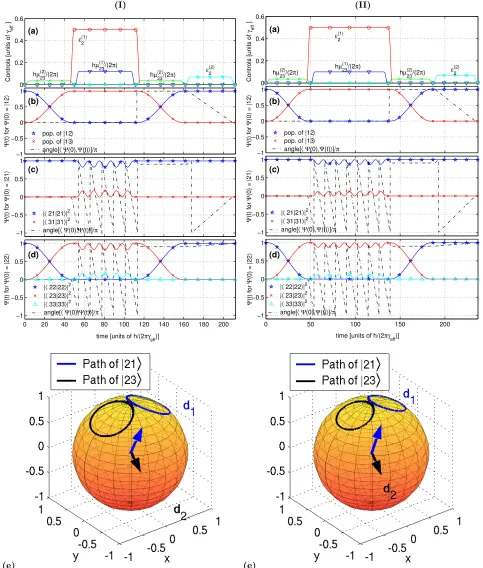
arbitrarily fast and the gate operation time would be lim-ited mainly by the time required to complete the second step, i.e., τ ≈ τ2 = 2π time units. In reality, however,
the gate operation time is usually limited by physical and technical constraints that impose, for instance, a min-imum pulse length τmin and maximum tunnelling rate µmax between the qubit and auxiliary quantum dot.
To explore the consequences of finite tunnelling rates and switching speeds, let us consider a specific example of a 2D charge qubit architecture as shown in Fig. 2 (a) with auxiliary quantum dots spaced about 2a= 170 nm apart [34]. Neglecting screening effects, the Coulomb en-ergy in this case is γeff ≈ 0.718 meV, and the
charac-teristic time scale~γ−1
eff ≈1 ps [35] Thus, theoretically,
two-qubit gate operation times of less then 20 ps could be achieved, as the previous sections show, and if one assumes that local operations can be realized arbitrarily fast then gate operation times of less than 7 ps would be possible.
However, if the pulse lengths must be & 50 ps — about the limit of what is accessible with current tech-nology — then Eq. (E1) shows that the best possible choice of the parameters n and k that satisfies this constraint while minimizing the gate operation time is
k = n = 5. The total gate operation time in this case increases to 3 × 50 + 18π ≈ 206.55 ps — as-suming we can achieve the required tunnelling rate of
µ(1)23 = (1/4)p
(10/9)2−1[γ
eff/~]≈1.21×1011rad s−1.
The evolution of the system for the resulting gate is shown in Fig. 9 (I).
If the maximum tunnelling rate that can be achieved (e.g., without applying control voltages that might lead to a breakdown of the oxide layer separating the silicon substrate and the surface control electrodes, or pulses that might result in population loss to higher-lying ex-cited states) are lower than this, then the gate operation time will be increased further. For example, if we must satisfyµ(1)23 ≤10−11 rad s−1 then Eqs. (E4), (E5) show
that the best choice for n and k is n = k = 7, which yieldsµ(1)23 ≈0.99×10¹¹rad s−1, and the gate operation
time increases to 231.68 ps, as shown in Fig. 9 (II).
VII. GATE ROBUSTNESS FOR NOISY CONTROLS
Another important issue in practice is the robustness of the gate for noisy controls. To study this effect we artificially added noise to our controls. Fig. 10 shows the increase of the gate errorEas a function of the magnitude of the noise added. The simulations were performed with a fixed time step of ∆t = 0.005, for which the average gate fidelity in the absence of noise exceeded 0.9999. The noise functionsη(t) were bounded
|η(t)| ≤η0 (20)
with Fourier transforms ˜η(ω) satisfying
|η˜(ω)| ≤
0 ω= 0
K/ω0 ω≤ω0 K/ω ω > ω0.
(21)
whereKis a constant. This type of noise corresponds to 1/f noise with a low-frequency cut-off, which is common in electronic devices.
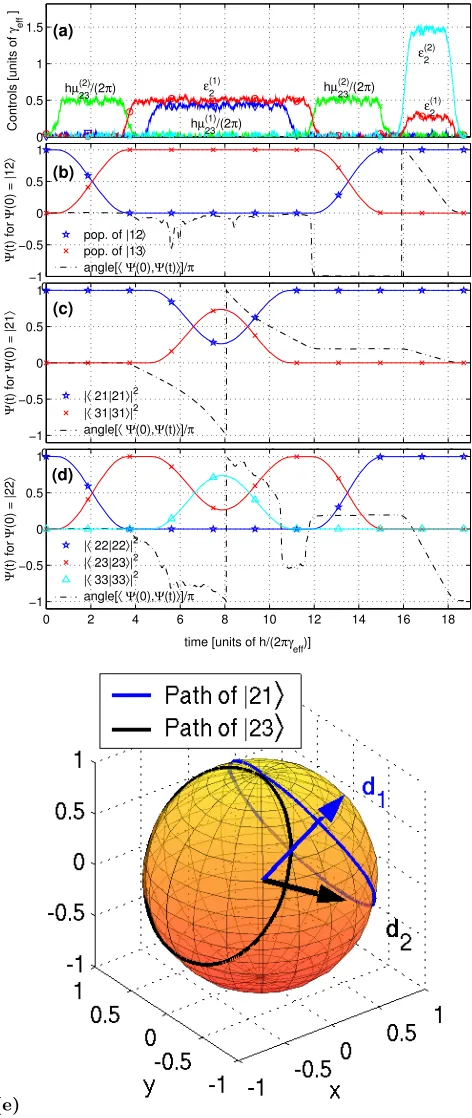
Although the addition of noise necessarily increase the gate error, the gate appears to be quite robust to this noise, as a typical example of the evolution of the system for noisy controls (Fig. 11) shows. Not unsurprisingly, the curves for varying threshold frequenciesω0in Fig. 10
suggest that the gate is more sensitive to low-frequency than high-frequency noise, as the high-frequency compo-nents tend to cancel.
VIII. GATE ROBUSTNESS FOR IMPERFECT
GEOMETRIES
A final issue that must be considered is the effect of manufacturing tolerances, which result in deviations of the qubit register from an ideal specification. In solid-state charge-based architectures of the types considered herein, the main issues appear to be imperfections in the placement or geometry of the quantum dots. The former is believed to be especially pronounced for quantum dots based on donor impurities in a Silicon matrix, while the latter will be relevant, e.g., for manufactured Ga/GaAs heterostructure quantum dots. As modelling all the pos-sible effects of imperfections in the fabrication process for heterostructure quantum dots would far exceed the scope of this paper, we shall focus on modelling the ef-fect of imperef-fect placement of the quantum dots on the gate performance.
For solid-state architectures based on donor impurities (e.g., Phosphorus) in a Silicon matrix the accuracy of placement of the donors is limited. In a shielded 2D ar-chitecture inaccurate placement of the donors will mainly cause variations in the tunnelling rates as the structure of the silicon lattice introduces spatial oscillations in the donor wavefunctions, and hence tunnelling rates [30] analogous to those seen in exchange systems [31, 32]. There will also be minor changes in the strength of the Coulomb interaction between the auxiliary sites. How-ever, the actual Coulomb coupling strengths and tun-nelling rates as a function of the control voltages ap-plied can, in principle, be determined using Hamilto-nian identification techniques similar to those described in Ref. [19]), for instance, and the control scheme can then easily be adapted to achieve the desired gate for the actual system.
(I) (II)
−1 −0.5 0 0.5 1
Ψ
(t) for
Ψ
(0) = |12
〉
pop. of |12〉 pop. of |13〉 angle[〈Ψ(0),Ψ(t)〉]/π
−1 −0.5 0 0.5 1
Ψ
(t) for
Ψ
(0) = |21
〉
|〈 21|21〉|2 |〈 31|31〉|2 angle[〈Ψ(0),Ψ(t)〉]/π
0 20 40 60 80 100 120 140 160 180 200 −1
−0.5 0 0.5 1
time [units of h/(2πγ
eff)]
Ψ
(t) for
Ψ
(0) = |22
〉
|〈 22|22〉|2 |〈 23|23〉|2 |〈 33|33〉|2 angle[〈Ψ(0),Ψ(t)〉]/π 0
0.2 0.4 0.6
Controls [units of
γeff
]
hµ23(2)/(2π) hµ
23 (2)/(2π)
hµ23(1)/(2π) ε2(1)
ε2(2) (a)
(b)
(c)
(d)
0 0.2 0.4 0.6
Controls [units of
γeff
]
−1 −0.5 0 0.5 1
Ψ
(t) for
Ψ
(0) = |12
〉
pop. of |12〉 pop. of |13〉 angle[〈Ψ(0),Ψ(t)〉]/π
−1 −0.5 0 0.5 1
Ψ
(t) for
Ψ
(0) = |21
〉
|〈 21|21〉|2 |〈 31|31〉|2 angle[〈Ψ(0),Ψ(t)〉]/π
0 50 100 150 200
−1 −0.5 0 0.5 1
time [units of h/(2πγeff)]
Ψ
(t) for
Ψ
(0) = |22
〉
|〈 22|22〉|2 |〈 23|23〉|2 |〈 33|33〉|2 angle[〈Ψ(0),Ψ(t)〉]/π
hµ23(2)/(2π) hµ23 hµ(2)23/(2π)
(1)/(2π)
ε
2 (1)
ε2(2) (a)
(b)
(c)
(d)
[image:10.612.66.549.54.622.2](e) (e)
FIG. 9: Control settings (a) and corresponding evolution of the initial states (b)|12i, (c)|21i, and (d)|22i, as well as evolution
of the two-level subsystems S and S′ on the Bloch sphere (e) under the operation of the controlled phase gate when (I)
minimum pulse length constraints ofτmin ≥50 ps necessitate n =k = 5, and (II) simultaneous pulse length and tunnelling
rate constraintsτmin≥50 ps andµ(1)23 ≤10−11rad s−1necessitaten=k= 7. Note the decrease in the angleθ1(increase inθ2)
between the rotation axisd1(d2) and the (positive)z-axis compared to then=k= 1 case, and the resulting greater difference
in the areas swept out by the Bloch vectorss1 (blue) ands2(black) in a single loop: π/5 versus 19π/5 in (I);π/7 versus 27π/7
in (II). Consequently, five and seven loops, respectively, are necessary to archive an area difference that is a multiple of 2π, and
the time required to implement the phase shift increases to 18π and 26π, respectively. Also note the slight distortion of the
loops near the north pole due to the dynamic change of the rotation axis during rise and decay periods of the pulses. Although
0.010 0.02 0.03 0.04 0.05 0.06 0.07 0.08 0.09 0.1 0.11 0.5
1 1.5 2 2.5 3 3.5
4x 10
−3
Magnitude of noise η
0
Average Error E (mean / min / max)
ω
0 = 25 (units of 2π/Tf)
ω
0 = 50 (units of 2π/Tf)
ω
0 = 75 (units of 2π/Tf)
ω0 = 100 (units of 2π/T
[image:11.612.321.557.52.611.2]f)
FIG. 10: Average gate error E as a function of the
magni-tudeη0of the noise for various threshold frequenciesω0. The
solid curves show the mean of Eand the error bars indicate
the range of E over 10 simulations. The data were plotted
horizontally offset to improve visual clarity.
the geometry, which cannot be compensated easily, even if they could be identified precisely, and perforce reduce the gate fidelity. To estimate the effect of such errors we have performed computer simulations. For a 3D ar-rangement of six quantum dots as shown in Fig. 2 (b), we randomly perturbed the positions of all six quantum dots by up to four lattice sites in thex- andy-directions, and ±1 monolayer in thez-direction, assuming a lattice con-stant of 0.3 nm, values that appear feasible with current fabrication technology [23], and numerically computed the average gate fidelity F for each perturbed system. Note that it was assumed here that the tunnelling rates can be kept steady despite the effect of the silicon lattice by adjusting the control voltages appropriately.
The numerical results in Table II suggest that the ro-bustness of our phase gate with respect to asymmetries depends significantly on the choice of interqubit spac-ings and the distance between the auxiliary sites. Con-cretely, the data suggest that the robustness of the gate with respect to random pertubations of the geometry is maximized by minimizing the distance between auxil-iary sites while maximizing the distances between qubits. There also appears to be a strong relation between the robustness with respect to asymmetries and the effec-tive Coulomb interaction between the auxiliary sites in the system, suggesting that maximizing the later quan-tity might be advantageous. However, it should be noted that stronger Coulomb coupling implies shorter gate op-eration times unless the gate parameters are changed, which might affect the gate fidelity. A final computa-tion for a (target) geometry with a = 20, b = 100 and
c = 10 showed that the average gate fidelity over 100 random perturbations ranged from 0.9944 to 1.0000 with
0 0.5 1 1.5
Controls [units of
γeff
]
0 2 4 6 8 10 12 14 16 18
−1 −0.5 0 0.5 1
Ψ
(t) for
Ψ
(0) = |12
〉
pop. of |12〉 pop. of |13〉 angle[〈Ψ(0),Ψ(t)〉]/π
0 2 4 6 8 10 12 14 16 18
−1 −0.5 0 0.5 1
Ψ
(t) for
Ψ
(0) = |21
〉
|〈 21|21〉|2 |〈 31|31〉|2 angle[〈Ψ(0),Ψ(t)〉]/π
0 2 4 6 8 10 12 14 16 18
−1 −0.5 0 0.5 1
time [units of h/(2πγeff)]
Ψ
(t) for
Ψ
(0) = |22
〉
|〈 22|22〉|2 |〈 23|23〉|2 |〈 33|33〉|2 angle[〈Ψ(0),Ψ(t)〉]/π hµ
23
(2)/(2π) hµ
23 (2)/(2π)
hµ23(1)/(2π) ε2(1)
ε2(2)
ε
2 (1)
(a)
(b)
(c)
(d)
(e)
FIG. 11: Control settings (a) and corresponding evolution of
the initial states (b) |12i, (c) |21i and (d) |22i, as well as
evolution of the two-level subsystemsS1andS2 on the Bloch
sphere (e) under the operation of our phase gate for noisy
controls (η0 = 0.1, ω0 = 50). The noise has no noticable
effect on the evolution of the populations. The relative phases exhibit some wiggles but they mostly seem to average out over the duration of the gate. The average gate error was
[image:11.612.58.292.54.251.2]a\b 30 50 70 90
20 0.964022 0.996631 0.998153 0.998855
40 N/A 0.909071 0.992692 0.998410
60 N/A N/A 0.831827 0.989618
[image:12.612.85.267.51.120.2]80 N/A N/A N/A 0.808333
TABLE II: Mean of the average gate fidelityF for different
geometries with fixed intra-qubit spacing ofc= 10 nm. For
each target geometry the mean of F was computed for 30
randomly perturbed systems. The gate parameters for all
simulations weren=k = 1 and the time steps were chosen
such that the average gate fidelity of eachunperturbed systems
was≥0.99995. Notice that the mean ofF increases sharply
for decreasing values ofa, and noticably for increasing values
ofb.
a mean (standard deviation) of 0.9989 (0.0013). These results suggest that even 3D charge-qubit architectures without shielding could be designed to be rather robust with respect to fabrication errors.
IX. CONCLUSIONS
We have presented two scalable achitectures for solid-state charge qubits that permit controlled entangling erations between pairs of qubits. We add that these op-erations could also be performed in parallel for cluster state preparation, a concept that we will explore else-where. The key feature of both geometries is that inter-actions between qubits are mediated via auxiliary quan-tum dots, while direct interactions between qubits are suppressed either through the use of shielding, or a three-dimensional design to cancel interactions. Controlled en-tangling gates can therefore be implemented by switching the charge distribution, and hence the Coulomb interac-tion, between qubits using the auxiliary dots. Both sys-tems should be realizable using existing or near-future fabrication techniques.
In particular, we have shown explicitly how to realize a controlled phase gate, i.e., a universal, maximally en-tangling two-qubit gate by a simple four-step procedure. The crucial step in the sequence is the controlled tun-nelling between a qubit state and an auxiliary dot, which induces a phase shift conditional on the occupation of an adjacent (auxiliary) quantum dot. The scheme is suffi-ciently flexible to accommodate practical constraints on both pulse lengths and tunnelling rates. Analysis of the gate operation shows that the controlled phase shift can be explained in terms of dynamic and geometric phases. Due to the strength of the Coulomb coupling the gate operation is surprisingly fast. In the absence of pulse length constraints gate operation times on the order of a few picoseconds would be theoretically possible, and even with currently realistic constraints on the pulse lengths and tunnelling rates, gate operation times around 200 ps should be attainable.
Using computer simulations, we have also studied the
effects of systematic errors on the gate performance. The simulations show that finite pulse rise and decay times tend to result in population loss to the auxiliary states, and can noticeably reduce the average gate fidelity. The average gate error increases sharply with increasing pulse rise and decay times. The ideal scheme, however, can easily be generalized to compensate for such system-atic errors. Simulations show that these corrections can greatly improve the average gate fidelity; the corrected pulse sequences always achieved average gate fidelities of
> 99.99%, and in some cases the average gate fidelity increased from∼70% without corrections to>99.99%. These results suggest that (experimental) characteriza-tion of the rise and decay times of the pulses is very important to achieve high gate fidelity.
We have also performed simulations to assess the ro-bustness of the gate to noisy control pulses. The re-sults suggest that the gate is quite robust with regard to both bandwith-limited 1/f noise and white noise. High-frequency noise tends to effectively cancel. Low-frequency fluctuations of the control pulses can reduce the gate fidelity. Surprisingly, however, the resulting av-erage gate errors are generally very small compared to the systematic errors. In most of our simulations, the average gate error increased only from<10−4 to < 10−3, even
for very noisy controls. Our simulations further suggest that even a 3D geometry without shielding, which relies mainly on symmetry to cancel the effect of the Coulomb interaction between qubits, can be made to be quite ro-bust to misalignment errors during fabrication if the pa-rameters of the geometry are chosen sufficiently carefully.
Acknowledgments
The authors thank C. J. Wellard (Univ. of Melbourne) for useful discussions. S.G.S and D.K.L.O acknowl-edge financial support from the Cambridge-MIT Insti-tute, Fujitsu and IST grants RESQ (IST-2001-37559) and TOPQIP (IST-2001-39215). S.G.S also acknowl-edges support from the EPSRC IRC in quantum infor-mation processing, and D.K.L.O thanks Sidney Sussex College for support. A.D.G is supported by the Aus-tralian Research Council, the AusAus-tralian government and the US National Security Agency (NSA), Advanced Re-search and Development Activity (ARDA) and the Army Research Office (ARO) under contract number DAAD19-01-1-0653, and acknowledges support from a Fujitsu visit-ing fellowship while visitvisit-ing the University of Cambridge.
APPENDIX A: LOCAL OPERATIONS
pa-rameter such as the energy difference ∆ǫ12= (ǫ2−ǫ1)/2
and the tunnelling rate µ12 between states |1i and |2i.
To see this note that we can rewrite Eq. (2) as follows:
ˆ
H(ǫd, µ12) = ¯ǫ12Iˆ12+∆ǫ12Zˆ12+~µ12Xˆ12+ǫ3|3ih3| (A1)
where ¯ǫ12 = (ǫ1+ǫ2)/2 and ˆZ12=|2ih2| − |1ih1|. Thus,
if we apply constant energy shifts ǫd and effect a fixed tunnelling rateµ12 between dots 1 and 2 (while all other
tunnelling rates are kept zero) for 0 ≤ t′ ≤ t then we
generate the unitary operator:
exp[−itHˆ(ǫd, µ12)/~]
=
cos(αt) ˆI12−isin(αt)
α~ (∆ǫ12Zˆ12+~µ12Xˆ12)
×
exp(−it¯ǫ12/~) + exp(−itǫ3/~)|3ih3| (A2)
where α = p(∆ǫ12/~)2+µ212. Thus, we can realize a
Hadamard transform, for instance, in a single step by setting ∆ǫ12=−~µ126= 0 for timet=π/(2
√ 2µ12).
APPENDIX B: FIRST SWAP OPERATION
The total Hamiltonian for the first swap operation is ˆ
H1= ˆH0+I3⊗Hˆ(2) where
ˆ
H(2) =~µ(2)23(|2ih3|+|3ih2|) (B1)
and ˆH0=|33ih33|as before. Applying this Hamiltonian
for time 0 ≤ t′ ≤ t gives rise to the unitary operator
ˆ
U1(t) = exp[−(it/~) ˆH1]. If we sett=τ1=π/(2µ(2)23) we
obtain the block-diagonal matrix ˆ
U(τ1) = diag(1,−iX,1,−iX,1, W) (B2)
whereX = 0 1
1 0
!
andW is a symmetric 2×2 matrix
with
W11 = e−iτ1/2
cosτ1u1 2
+ i
u1
sinτ1u1 2
W12 = e−iτ1/2
"
−2iµ (2) 23 u1
sinτ1u1 2
#
W22 = e−iτ1/2
cosτ1u1 2
−ui
1sin
τ1u1
2
and u1 =
q
1 + 4[µ(2)23]2. Uˆ
1(t1) swaps the population
of states |2i2 and |3i2 provided that state |3i1 is not
occupied.
APPENDIX C: SECOND SWAP OPERATION
The total Hamiltonian for the second gate is ˆH2 =
ˆ
H0+ ˆH(1)⊗I3 where
ˆ
H(1)= 1
2|2ih2|+~µ
(1)
23(|2ih3|+|3ih2|) (C1)
and ˆH0=|33ih33|as before. Applying this Hamiltonian
for time 0 ≤ t′ ≤ t gives rise to the unitary operator
ˆ
U2(t) = exp[−(it/~) ˆH2], which has the general form
ˆ
U2(t) =
I3 0 0
0 A B
0 B C
(C2)
where A = diag(a, a, a′), B = diag(b, b, b′) and C =
diag(c, c, c′). We must choose the gate operation time
τ2 such thatB= 0, i.e.,b=b′ = 0. Since
b = −4iexp
−it
4
µ(1)
23 u2
sin
u
2t
4
(C3)
b′ = −4iexp
−3it
4
µ(1)
23 u2
sin
u
2t
4
(C4)
with u2 =
q
1 + 16[µ(1)23]2, this is equivalent to u 2T2 =
4nπfor some integern, or
τ2=
4πn q
1 + 16[µ(1)23]2
. (C5)
This choice of gate operation time gives
U2(τ2) = diag(1,1,1, a, a, a′, a, a, a′) (C6)
where we have
a = (−1)nexp(−inπ/u 2), a′ = (−1)nexp(−i3nπ/u
2).
(C7)
APPENDIX D: LOCAL PHASE ROTATIONS
Composing the three swap operations, noting ˆU3(τ3) =
ˆ
U1(τ1), gives
ˆ
U = ˆU1(τ1) ˆU2(τ2) ˆU1(τ1)
= diag(1,−1,−1, a,−a′,−a, a, Wdiag(a, a′)W)
(D1)
whose projection onto the two-qubit subspace
{|11i,|12i,|21i,|22i} is ˜U = diag(1,−1, a,−a′) with a
anda as in (C7), which is not quite a controlled phase gate yet. However, if we multiply ˜U by U(1) ⊗U(2),
where
U(1) = diag (1,(−1)nexp(iπn/u 2)),
U(2) = diag(1,−1) (D2)
which corresponds to simultaneous local phase rotations on state|2i1 and|2i2, we obtain
whereu2=
q
1 + 16[µ(1)23]2 and
µ(1)23 =
1 4
s
2n
2k−1
2
−1 (D4)
for positive integersnandksatisfying 2n >2k−1. Then clearly 2πn= (2k−1)πu2, i.e., we have
U(1)⊗U(2)U˜ = diag(1,1,1,−1) = ˆUphase. (D5)
To achieve a controlled phase gate on the qubit space we thus require
exp(−i2πn/u2) =−1 ⇔ 2πn= (2k−1)πu2. (D6)
Substituting u2 = 2n/(2k−1) yields (−1)neiπn/u2 = eiπ(n+k−1/2), which shows that ˆU(1)= ˆU(1)
2 (ℓπ) withℓ=
1/2−(n+k) mod 2 and ˆU(2) = ˆU(2)
2 (π), i.e., we must
set ǫ(1)2 =ℓπ/τ4 andǫ2(2) =π/τ4 for some timet=τ4 in
the final step.
APPENDIX E: TUNNELLING RATE AND PULSE LENGTH CONSTRAINTS
In absence of constraints on the tunnelling rateµ(1)23 it is easy to see that the optimal choice of the parametersn
andkin the second step isk=n= 1, which impliesu2=
2 and µ(1)23 =
√
3/4. In practice, however, the control
pulses usually cannot be arbitrarily short and there the tunnelling rates cannot be made arbitrarily large, and we can accommodate these constraints by choosing suitable values for the parametersnandk.
If the mimimum pulse length is τ2 ≥ Tmin but the tunnelling rates are unconstrained then we simply set
k=
τmin
4π +
1 2
, n=k. (E1)
where⌈x⌉is the smallest positive integer≥x, to optimize the gate operation time while satisfying the pulse length constraint.
If we must satisfy µ(1)23 ≤ µmax but there is no con-straint on the length of the control pulses, we set
k =
(umax−1)−1
/2
+ 1 (E2)
n = ⌊(2k−1)umax/2⌋ (E3)
whereumax=
p
16µ2
max+ 1 and⌊x⌋is the largest (pos-itive) integer≤x, to satisfy the constraint and optimize the gate operation time.
Finally, if we must satisfy τ2≥τmin andµ(1)23 ≤µmax, we choose
k = max{k1,⌈τmin/4π+ 1/2⌉} (E4)
n = ⌊(2k−1)umax/2⌋ (E5)
where k1 = (umax−1)−1/2 + 1 as in (E2) and
umax=
p
16µ2
max+ 1 as before.
[1] D. P. DiVincenzo, Science270, 255 (1995).
[2] A. Barenco andet al., Phys. Rev. A52, 3457 (1995).
[3] D. Loss and D. P. DiVincenzo, Phys. Rev. A 57, 120
(1998).
[4] B. E. Kane, Nature393, 133 (1998).
[5] R. Vrijenet al., Phys. Rev. A62, 012306 (2000).
[6] L. C. L. Hollenberg et al., Phys. Rev. B 69, 113301
(2004).
[7] R. G. Clark and et al., Philos. Trans. R. Soc. London,
Ser. A361, 1451 (2003).
[8] T. Schenkelet al., J. Appl. Phys.94, 7017 (2003).
[9] A. K. Ekert and R. Jozsa, Rev. Mod. Phys. 68, 733
(1996).
[10] L. Fedichkin, M. Yanchencho, and K. A. Valiev,
Nan-otechnology11, 387 (2000).
[11] T. Hayashiet al., Phys. Rev. Lett.91, 226804 (2003).
[12] Y. Nakamura, Y. A. Pashkin, and T. S. Tsai, Nature
398, 786 (1999).
[13] M. H. Devoret and R. J. Schoelkopf, Nature 406, 1039
(2000).
[14] A. D. Greentree et al., Phys. Rev. Lett. 92, 097901
(2004).
[15] Y. A. Pashkinet al., Nature421, 823 (2003).
[16] S. Lloyd, Science261, 1569 (1993).
[17] S. C. Benjamin, Phys. Rev. Lett.88, 017904 (2001).
[18] S. C. Benjamin and S. Bose, Phys. Rev. Lett.90, 247901
(2003).
[19] S. G. Schirmer, A. Kolli, and D. K. L. Oi, Phys. Rev. A
69, 050603(R) (2004).
[20] S. Lloyd, Phys. Rev. Lett.75, 346 (1995).
[21] W. G. van der Wielet al., Rev. Mod. Phys.75, 1 (2003).
[22] K. Ono, D. G. Austing, Y. Tokura, and S. Tarucha,
Sci-ence297, 1313 (2002).
[23] S. R. Schofieldet al., Phys. Rev. Lett.91, 136104 (2003).
[24] J. R. Tucker and T.-C. Shen, Quantum Inf. Comput.1,
129 (2001).
[25] A. D. Greentree, A. R. Hamilton, and F. Green, Phys.
Rev. B70, 041305(R) (2004).
[26] Y. Aharonov and J. Anandan, Phys. Rev. Lett.58, 1593
(1987).
[27] J. F. Poyatos and J. I. Cirac, Phys. Rev. Lett.78, 390
(1997).
[28] M. D. Bowderyet al., Phys. Lett. A294, 258 (2002).
[29] S. G. Schirmer, A. D. Greentree, V. Ramakrishna, and
H. Rabitz, J. Phys. A35, 8315 (2002).
[30] C. J. Wellard, Private Communication, 2004.
[31] B. Koiller, X. Hu, and S. Das Sarma, Phys. Rev. Lett.
88, 027903 (2002).
[32] C. J. Wellardet al., Phys. Rev. B68, 195209 (2003).
[33] These figures are for numerical simulations with time step
∆t = 0.005 and can be improved further by decreasing
[34] This value seems realistic to allow for a metal barrier sufficiently thick to provide adequate screening and suffi-cient distance between the quantum dots and the barrier to minimize barrier-induced decoherence.