UNIVERSITI TEKNIKAL MALAYSIA MELAKA
SINGLE PHASE CAPACITOR CLAMPED MULTILEVEL
INVERTER
This report submitted in accordance with requirement of the Universiti Teknikal Malaysia Melaka (UTeM) for the Bachelor Degree of Electrical Engineering
Technology (Industrial Power)(Hons.)
by
AHMAD HAFIZ BIN AYOB B071110012
920423115355
UNIVERSITI TEKNIKAL MALAYSIA MELAKA
BORANG PENGESAHAN STATUS LAPORAN PROJEK SARJANA MUDA
TAJUK: SINGLE PHASE CAPACITOR CLAMPED MULTILEVEL INVERTER
SESI PENGAJIAN: 2014/15 Semester 7
Saya AHMAD HAFIZ BIN AYOB
mengaku membenarkan Laporan PSM ini disimpan di Perpustakaan Universiti Teknikal Malaysia Melaka (UTeM) dengan syarat-syarat kegunaan seperti berikut:
1. Laporan PSM adalah hak milik Universiti Teknikal Malaysia Melaka dan penulis. 2. Perpustakaan Universiti Teknikal Malaysia Melaka dibenarkan membuat salinan
untuk tujuan pengajian sahaja dengan izin penulis.
3. Perpustakaan dibenarkan membuat salinan laporan PSM ini sebagai bahan pertukaran antara institusi pengajian tinggi.
4. **Sila tandakan ( )
SULIT
TERHAD
TIDAK TERHAD
(Mengandungi maklumat yang berdarjah keselamatan atau kepentingan Malaysia sebagaimana yang termaktub dalam AKTA RAHSIA RASMI 1972)
(Mengandungi maklumat TERHAD yang telah ditentukan oleh organisasi/badan di mana penyelidikan dijalankan)
Alamat Tetap:
Lot 2762, Kampung Bukit Petiti, Manir 21200 Kuala Terengganu,
Terengganu
Tarikh: ________________________
Disahkan oleh:
Cop Rasmi:
Tarikh: _______________________
FAKULTI TEKNOLOGI KEJURUTERAAN
Tel : +606 234 6623 | Faks : +606 23406526
Rujukan Kami (Our Ref) : Rujukan Tuan (Your Ref) :
01JAN 2015 Pustakawan
Perpustakaan UTeM
Universiti Teknikal Malaysia Melaka Hang Tuah Jaya,
76100 Durian Tunggal, Melaka.
Tuan/Puan,
PENGKELASAN LAPORAN PSM SEBAGAI SULIT/TERHAD LAPORAN PROJEK SARJANA MUDA TEKNOLOGI KEJURUTERAAN ELEKTRIK (KUASA INDUSTRI): AHMAD HAFIZ BIN AYOB
Sukacita dimaklumkan bahawa Laporan PSM yang tersebut di atas bertajuk “Single Phase Capacitor Clamped Multilevel Inverter” mohon dikelaskan sebagai *SULIT / TERHAD untuk tempoh LIMA(5) tahun dari tarikh surat ini.
2. Hal ini adalah kerana IANYA MERUPAKAN PROJEK YANG DITAJA OLEH SYARIKAT LUAR DAN HASIL KAJIANNYA ADALAH SULIT.
Sekian dimaklumkan. Terima kasih.
Yang benar,
________________
DECLARATION
“I hereby declare that the content in this project is the result of my own work expect references and citations which I have clearly stated the source of origin”
Signature : ………
Name : AHMAD HAFIZ BIN AYOB Date : 20TH DEC 2014
ii
APPROVAL
This report is submitted to the Faculty of Engineering Technology of UTeM as a partial fulfillment of the requirements for the degree of Bachelor of Electrical Engineering Technology (Industrial Power) with Honors. The member of the supervisory committee is as follow:
iii
ABSTRAK
iv
ABSTRACT
v
DEDICATION
vi
ACKNOWLEDGEMENT
First and foremost, I would like to take this golden opportunity to express my appreciation to my final year project supervisor, Miss Suziana for being a dedicated lecturer guiding me through this project to run smoothly. This project cannot be completed and perfected if without the valuable suggestion and useful information from my supervisor. Her patience and enthusiastic in guided me through this final year project have gave me a great courage in completing this project.
Apart from that, I also would like to thanks to my lecturers and all my friends for the helped in giving me their morals support during this project development and also shared some information with regards to the multilevel inverter and the software guide.
Last but not least, I would like to express my deepest love and gratitude to my beloved parents for giving me unlimited encouragement during my studies in University Technical Malaysia Malacca (UTeM).
vii
TABLE OF CONTENTS
DECLARATION i
APPROVAL ii
ABSTRAK iii
ABSTRACT iv
DEDICATION v
ACKNOWLEDGEMENT vi
LIST OF TABLES ix
LIST OF FIGURES x
LIST OF ABBREVIATIONS, SYMBOLS AND NOMENCLATURE xi
CHAPTER 1 1
1.1 Background 1
1.2 Problem Statement 2
1.3 Objective of Project 3
1.4 Scope of Study 3
CHAPTER 2 4
2.1 Inverter 4
2.2 Voltage Source Inverter 5
2.3 Multilevel Inverter (MLI) 6
2.3.1 Capacitor Clamped Multilevel Inverter 6
2.3.2 Diode Clamped Multilevel Inverter 7
2.3.3 Cascade H-Bridge Multilevel Inverter (CHMI) 8
2.4 Switching Device 8
2.5 Pulse Width Modulation (PWM) 9
2.6 Total Harmonic Distortion (THD) 10
CHAPTER 3 11
3.1 Process Flow Chart 11
3.2 Circuit Development 13
3.2.1 Matlab/Simulink 14
3.2.2 Proteus 16
viii
3.3 Hardware Implementation 18
3.3.1 Etching Process 18
3.3.2 Soldering Process 22
3.3.3 Testing Connection Process 23
3.3.4 Driver 23
3.3.5 The MOSFET 24
3.3.6 Microcontroller 25
3.3.7 Troubleshooting 25
3.3.8 Bill of Materials (BOM) 27
3.4 Report Writing 27
CHAPTER 4 28
4.1 Simulation Development Results and Discussion 28
4.2 Hardware Development Results and Discussion 30
CHAPTER 5 33
5.1 Conclusion 33
5.2 Future Work 34
5.3 Commercialization 34
REFERENCES 35
APPENDICES 37
APPENDIX A 38
Calculations 38
APPENDIX B 40
Gantt Charts 40
APPENDIX C 41
ix
LIST OF TABLES
Tables Title Page
Table 2.1: The Switching State 7
Table 3.2: BOM 27
x
LIST OF FIGURES
Figure Title Page
Figure 2.1: Inverter 4
Figure 2.2: The VSI Segment. 5
Figure 2.3: The MOSFET. 9
Figure 2.4: Pulse Width Modulation Waveform. 9
Figure 3.5: THD Setup. 16
Figure 3.6: The Scematic Drawing for CCMI. 16
Figure 3.7: The PCB Drawing for CCMI. 17
Figure 3.8: The Microcontroller. 18
Figure 3.9: Printed PCB. 19
Figure 3.10: UV Curing Machine. 19
Figure 3.11: Cleaning Process. 20
Figure 3.12: Photoresist Stripper. 21
Figure 3.13: Board Being Dried. 21
Figure 3.14: Drilling Process. 22
Figure 3.15: The Complete Soldering. 23
Figure 3.16: The Driver. 24
Figure 3.17: The MOSFET. 24
Figure 3.18: Microcontroller F2808. 25
Figure 3.19: The Troubleshooting of Driver. 26
xi
LIST OF ABBREVIATIONS, SYMBOLS AND
NOMENCLATURE
IGBT – Insulated Gated Bipolar Transistor THD – Total Harmonic Distortion
MOSFET – Metal Oxide Semiconductor Field Effect Transistor PWM – Pulse Width Modulation
AC – Alternating Current DC – Direct Current MLI – Multilevel Inverter
CCMI – Capacitor Clamped Multilevel Inverter CCS – Code Composer Studio
1 Chapter 1 will explained on the background research of this project research. This chapter will also include the problem statement, the objectives, scope, and project significance.
1.1 Background
Multilevel inverter is an alternative structure to the conventional power inverter. Multilevel inverter’s operation depends on the structure and the number of the power switches in the inverter. The main feature of the multilevel inverter is it has the ability to reduce the voltage stress on each of the multiple levels in DC bus of the circuit. It also has smaller distortion in the multilevel inverter AC side waveform can be achieved even though at low switching frequency. Besides, switching losses in the inverter are reduced by the increased flexibility for voltage waveform produced by increasing number of voltage level. There are three main types of the multilevel inverter topology, capacitor clamped, diode clamped and cascaded multilevel inverter.
Capacitor clamped multilevel inverter involves in the usage of extra capacitor clamped to the power switches phase rail to provide the DC voltage level. This structure allow for the inverter to supply high capabilities especially during the power outages due to the redundancy in switching states provided by the clamping capacitor. This type of multilevel inverter also provides the switching combination redundancy that is very useful for the voltage level balancing. In this project we are
2 using pulse width modulation (PWM) strategies. As the switches, the project is using MOSFET. This is because MOSFET are low power consumption and dissipation, low waste heat, and low mass production costs. In the project, the five level output with sixteen MOSFET is constructed.
1.2 Problem Statement
Due to current source inverter has slower dynamic response and big in size, it may cause main problem in power application. In additional, voltage of CSI need to be maintained continuously and causes a complexity system while reduce its reliability. Besides that, voltage source inverter has decreasing power factor with decreasing speed. This type of inverter also has induced harmonics.
3
1.3 Objective of Project
The objectives of this project are as follows:
i. To study a single phase capacitor clamped multilevel inverter. ii. To simulate a proposed topology using Matlab/Simulink. iii. To implement the hardware of the proposed topology.
1.4 Scope of Study
4 Literature review is a review of a research that has been made regarding the particular problem that has been identified and needs to be solved. This review should describe summarize, evaluate and clarify the project. It also goes beyond the search for information and includes the identification and articulation of relationships between the literature and the field of research.
In this chapter 2, reviews of the previous researches project that are related with this project research will be discussed. The information will be become additional source for the project to make some improvement and more successful. To have a brief understanding of the researches related to the project, a few literature reviews had been done.
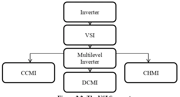
2.1 Inverter
The inverter is an electrical device which converts DC input voltage to AC output voltage. Figure 2.1 shows that DC converts to AC using inverter (Mailah, F. Nashiren et al. 2010).
LITERATURE REVIEW
CHAPTER 2
Direct Current Alternating Current
[image:19.595.128.534.652.728.2]Inverter
5 The DC source can be the voltage or current source, it is VSI and CSI. Inverters allowing portability by providing the AC power in areas where only batteries can make it available. Figure 2.2 below shows the course of VSI segment.
2.2 Voltage Source Inverter
DC voltage source for the input of the inverter means that the inverter is a voltages source inverter (VSI). VSI circuit has direct control over output and the shape of voltage waveforms output should be vary to the load that connected at the output.
The advantages of VSI as the following (Bogdan M. Wilamowski et al. 2011):
i. Good speed range. ii. Simple regulator design.
The disadvantages of VSI as the following:
i. Decreasing power factor with decreasing speed. ii. Induced harmonics.
VSI Inverter
Multilevel Inverter CCMI
DCMI
[image:20.595.145.510.155.353.2]CHMI
6
2.3 Multilevel Inverter (MLI)
Multilevel inverter is an alternative way to the conventional power converter that had been accepted and used in many applications (Rashid, M. H et al. 2004). The structure and the number of the power switches in the inverter circuit affected its operation. The performance of the inverter can be improved by increasing the number of the power switches in the circuit (A. Tahri, A. Draou and M. Ermis). The main feature of the multilevel inverter is it has the ability to reduce the voltage stress on each of the power switches. Besides, smaller distortion in the multilevel inverter AC side waveform can be achieved even though at low switching frequency.
There are three main type of the multilevel inverter topology (Mailah, F. Nashiren et al. 2010):
i. Cascaded Multilevel Inverter (CMI)
ii. Diode Clamped Multilevel Inverter (DCMI) iii. Capacitor Clamped Multilevel Inverter (CCMI)
2.3.1 Capacitor Clamped Multilevel Inverter
CCMI involves in the usage of extra capacitor clamped to power switches to provide the DC voltage level. This structure allows for the inverter to supply high capabilities especially during the power outages due to the redundancy in switching states provided by the clamping capacitor. This type of multilevel inverter inverters also provides the switching combination redundancy that is very useful for the voltage level balancing.
The advantages of CCMI as the following (Mailah, F. Nashiren et al. 2010):
i. Does not requiring diode clamping.
7 iii. Phase redundancies are available for balancing the voltage levels of the
capacitors.
iv. The big number of capacitors enables the inverter to ride through short duration outages and deep voltage stages.
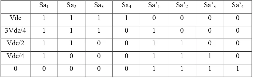
[image:22.595.110.532.259.389.2]The switching state is the most crucial part in the CCMI topology. So after the studied on CCMI, Table 2.1 shows the switching combination.
Table 2.1: The Switching State
Sa1 Sa2 Sa3 Sa4 Sa’1 Sa’2 Sa’3 Sa’4
Vdc 1 1 1 1 0 0 0 0
3Vdc/4 1 1 1 0 1 0 0 0
Vdc/2 1 1 0 0 1 1 0 0
Vdc/4 1 0 0 0 1 1 1 0
0 0 0 0 0 1 1 1 1
2.3.2 Diode Clamped Multilevel Inverter
Diode clamped multilevel inverter (DCMI) using the diode as the clamping device to clamp the DC bus voltage to achieve the level of output voltage.
The advantages of DCMI as the following (Khomfoi, S. and Tolbert, L. M. 2007):
i. The efficiency of the inverter is high because all devices are switched at the fundamental frequency.
ii. The total harmonic contain is very low when the number of level is high to avoid from filtered.
8 The disadvantages of DCMI as the following:
i. The excessive clamping diode is required when the number of level is high.
ii. The real power of individual converter is hard to control in MLI system.
2.3.3 Cascade H-Bridge Multilevel Inverter (CHMI)
Cascade H-bridge multilevel inverter is using a series of single phase full bridges makes up a phase for the inverter.
The advantages of CHMI as the following (Prattipati, J. and Kommukuri, V.S. 2012):
i. Lesser components needed to design the same number of voltage level compared to DCMI and CCMI.
ii. Since each H-bridge has the same structure, modularized circuit layout and packaging are possible.
iii. No need extra clamping diode and voltage balancing capacitor.
The disadvantages of CHMI as the following:
i. Separate dc sources are required, resulting in limited applicability.
2.4 Switching Device
9 (MOSFET). For this project MOSFET have been chose instead of IGBT because of voltage level for MOSFET is lower than IGBT. Furthermore, the price for MOSFET is cheaper than the IGBT. MOSFET have low power consumption and dissipation, low heat waste and low mass production costs (Josefsson, O. 2013). Figure 2.3 shows the type of MOSFET that been used in this project.
Figure 2.1: The MOSFET
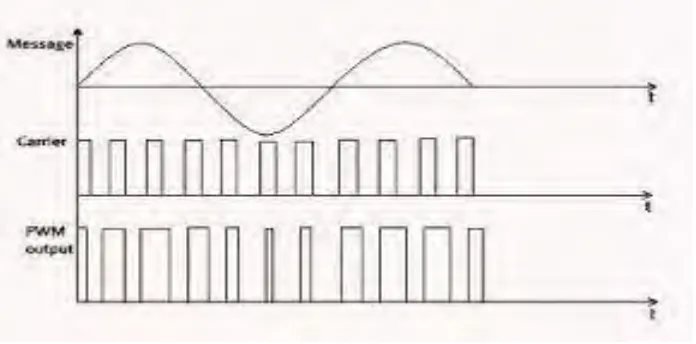
2.5 Pulse Width Modulation (PWM)
Pulse width modulation is usually used as switching technique. For industrial purposed, the control of voltage output is important to adjust with variation of dc input voltage, to regulate voltage inverter and satisfy the contain volts and frequency requirement (A. Tahri, A. Draou and M. Ermis). Figure 2.4 shows the PWM waveform.
[image:24.595.147.495.534.706.2]