Rochester Institute of Technology
RIT Scholar Works
Theses
Thesis/Dissertation Collections
7-2005
Modeling of a hardware VLSI placement system:
Accelerating the Simulated Annealing algorithm
William Merle Batts Jr.
Follow this and additional works at:
http://scholarworks.rit.edu/theses
This Thesis is brought to you for free and open access by the Thesis/Dissertation Collections at RIT Scholar Works. It has been accepted for inclusion in Theses by an authorized administrator of RIT Scholar Works. For more information, please [email protected].
Recommended Citation
Modeling of a Hardware VLSI Placement System:
Accelerating the Simulated Annealing Algorithm
by
William Merle Batts Jf.
A Thesis Submitted in Partial Fulfillment of the Requirements for the Degree of
Master of Science in Computer Engineering
Supervised by
Visiting Assistant Professor of Computer Engineering Dr. Marcin Lukowiak
Department of Computer Engineering
Kate Gleason College of Engineering
Rochester Institute of Technology
Rochester
,
New York
July 2005
Approved By:
Marcin tukowiak
Dr. Marcin Lukowiak
Visiting Assistant Professor of Computer Engineering
Primary Adviser
Stanisfaw Radziszowski
Dr
.
Stanislaw Radziszowski
Professor of Computer Science
Greg P. Semeraro
Dr
.
Greg Semeraro
Thesis Release Permission Form
Rochester Institute of Technology
Kate Gleason College of Engineering
Title: Modeling of a Hardware VLSI Placement System: Accelerating
the Simulated Annealing Algorithm
I, William Merle Batts Jr.,
hereby grant permission to the Wallace Memorial Library to
reproduce my thesis in whole or part.
William Merle Batts Jr.
William Merle Batts Jr.
7
c9f
-
!)5
Dedication
Forall ofmy friends and
family,
especiallyDenise,
whoseunwavering supportmade thisAcknowledgments
I'dliketo thankmyadviserDr. Marcin Lukowiakfor hisguidance, wisdom andunending
patience. Fd also liketo thankmy committee members Dr. Stanislaw Radziszowskiand
Dr.
Greg
Semeraro,
whoseinputandtimegivento thisworkisgreatlyappreciated.Abstract
An essential step in the automation ofelectronic design is the placement ofthe physical
componentsonthetarget semiconductordie. Theplacement steppresents theopportunity
toreducecostsintermsofwirelengthandperformance
degradation;
howeverit iscompute intensive andis NP-complete interms ofobtaining an optimal solution. As designs havegrown in complexity and gate count, obtaining an optimal solution is not feasible due to time to market constraintsor sheer compute effort required. Heuristicalgorithms allowfor
efficient but sub-optimal designs to be produced with a reduction in processing time. A widelyused algorithmisSimulated
Annealing
(SA).The goal ofthis work was to
develop
a modelthat would enable an analysis into thefeasibility
ofdeveloping
a hardware accelerated placement system which uses SA at itscore. The SA heuristicwas analyzed for possible improvements in efficiency with focus given to
targeting
the system forhardware. A solutionimplementing
parallel computing with specialized hardware configurations inside a field programmable gate array(FPGA)
was investigatedashaving
the possibilityto improvethe efficiencyofthe SA-basedalgo rithm. All supportingsubsystems were alsodescribed forahardware accelerated model.Alarge speedupwas analyticallyshown from both acceleratingthecritical path ofthe SA algorithm aswell as novel methods of
improving
SA'sefficiency. Asdata throughputContents
Dedication iii
Acknowledgments iv
Abstract v
Glossary
xii1 Introduction 1
2 Motivation 3
3 Background 5
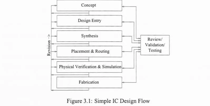
3.1 ICDesignFlow 5
3.1.1 Concept - Research& Development 6
3.1.2 Concept- High Level Design 6
3.1.3 Design
Entry
73.1.4 Synthesis 7
3.1.5 Placement &
Routing
83.1.6 Physical Verification & Simulation 9
3.1.7 Fabrication 10
3.2 ElectronicDesign Automation 10
3.2.1 Logical Description 11
3.2.2 Structural Description 15
3.3
Library
Exchange Format/DesignExchangeFormat 163.3.1 LEFSyntax 16
3.3.2 DEFSyntax 18
3.4 PhysicalDesign Automation 20
3.4.1 Placement 21
3.4.2
Routing
233.4.3 Back Annotation 24
4 Placement 25
4.1 Exhaustive Search 27
4.2 GeneralizedHill Climbing/Local Search 28
4.3 Min-Cut 29
4.4 Genetic Algorithms 30
4.5 Tabu Search 30
5 Simulated
Annealing
325.1 Physical Model 32
5.2 ApplicationtoCombinatorial Optimization 33
5.3 SA& Placement 33
5.4 SA Research 37
5.4.1 Parallel SA 38
5.4.2 HardwareAssisted SA 39
5.4.3
Greedy
Mixed Perturbations 405.4.4 Multiple HeuristicCombination 41
6 SoftwareImplementation 43
6.1 Software RevisionsandLessons Learned 43
6.1.1 Experimental Code 43
6.1.2 Initial LEF/DEF Placements 45
6.1.3 Benchmarks 46
6.2 Logical Modules 46
6.2.1 LEF/DEF Reader & Writer 47
6.2.2 Design Perturbation 48
6.2.3 Wirelength Estimator 49
6.2.4
Overlap
Calculation 506.2.5 MoveAcceptance 51
6.2.6 Design Update 51
6.2.7 Temperature Update 52
6.3 Temperature Schedule 52
6.4 BenchmarkCircuits 54
6.5 Characterization & Optimization 55
7 HardwareModel 61
7.1 Wire Length Estimator 61
7.2
Overlap
Detector 637.3 MoveAcceptance Logic 65
7.4 Interfaces 66
7.4.1 DatapathControl 67
7.4.2 Component
Supply
687.4.3 Design Update & Algorithm Management 69
8 MethodofInvestigation 70
9 Results 72
9.1 SoftwareImplementation 72
9.2 Hardware Model 74
9.3
Speedup
Justification 7410 Conclusions 77
10.1 Discussion 77
10.2 Future Work 78
10.2.1 Software Implementation 79
10.2.2 Control Unit 79
10.2.3 Data Management 79
10.3
InClosing
80Bibliography
81List
of
Figures
3.1 Simple IC Design Flow 5
3.2 One-bit Adder Example VHDL Description 12
3.3 One-bit Adder Logical Schematic 12
3.4 LEF Syntax for
SIZE-only
MACRO Statement 173.5 Example LEF Definitionof aOne-Bit Adder's Components 17 3.6
Bounding
Box Wirelength EstimationandOverlap
Penalty
183.7 DEF Syntax for Simple Net
listing
193.8 Example DEF Definitionof aOne-Bit Full Adder 20
3.9 One-bit Adder Initial Random Placement 21
3.10 One-bit Adder Final Placement 22
3.11 Example DEF Definition of aOne-Bit Full Adder 23
4.1 Seriesof
Neighboring
SolutionsContaining
aLocal Minimum 295.1 Molecules' MovementsperTemperature Region 32
5.2 Simulated
Annealing
Placement FlowChart 345.3
Bounding
Box Wirelength EstimationandOverlap Penalty
35 5.4 CharacteristicsJustifying
FPGA Application 406.1 Initial Software Algorithm Organization 44
6.2 Software Module Interaction 47
6.3 Sample Temperature Schedule 53
6.4 SoftwareSA Placement Time Profile 56
6.5 Software SA Placement Costvs. Iteration 58
6.6 InitialandFinal Placements ofBenchmark ibm05 60
7.1
Top
LevelRTLSchematic 627.2 WirelengthEstimator RTLSchematic 64
7.3
Overlap
Detector RTL Schematic 657.4 Move AcceptanceLogicRTL Schematic 66
8.1 Test
Method
List
of
Tables
6.1 Benchmark ibmO 1 - ibm04 Information 55
6.2 Benchmark ibm01-ibm04 Time Profiles (%
total)
556.3 Cost Delta Function Time Analysis 57
6.4 Average Cost Delta Function Composite Analysis 57
7.1
Top
Level Hardware Input Interface 637.2
Top
Level Hardware OutputInterface 649.1 TimeComparisontoaMature Placement Tool 73
9.2 DieGrid PointsperBenchmark 74
9.3 FPGAClock Cycle RequirementperCalculation 75
Glossary
ASIC Application Specific Integrated Circuit- An IC
whichhas beenconstructedto
perform alimitedrange offunctionsveryefficiently,usuallyfasterthanaGPP. Its
functionality
cannotbechangedafterit has beenmanufactured.CAD Computer Aided Design
-Designworkmanaged and enchanced
by
theuse ofcomputertechnology.
component Aunitwhich provides sometypeof
functionality
toahardware designandmay be combined with other units to implementmore complicated behavior. An adder is a common example of a component, providing the ability to add
twovalues withtheabilitytobecombinedinto a larger
design,
such as a mul tiplier.D
DEF Design Exchange Format
-An ASCII textbased format which defines a de
sign's specific organization interms ofinstances of components andintercon
nections. Used in conjunction with LEF. A community project organized
by
the Silicon Integration Initiative(SI2).die Thesemiconductortarget on whichintegratedcircuits are constructed.
E
EDA ElectronicDesign Automation- A CADtechnique
allowingthedesign flowof electronicdevicestobecomemoremanagable,reducingassociated overhead.
FPGA Field Programmable Gate
Array
-A digital processing device which has the
abilitytobe programmed afterit ismanufactured allowing its
functionality
to bechanged.FSM Finite State Machine- Logic
whichconsists of afinite number of states with transitions and outputs defined
by
the current state and possibly the value ofinputs.
G
GPP General Purpose Processor
-Aprocessor whichimplements
functionality
throughgroupsofinstructionsand genericfunctional units ratherthan specializeddata structures.
H
HPWL Half Perimeter Wire Length- A
method ofapproximatinga net's interconnec tionwirelength
by
fully
enclosing itinaminimalbounding
box andtaking
halfoftheperimeter.
I
IC Integrated Circuit - A
general term for an electronic device which contains active semicondictor switches andpossiblypassive devicessuch as resistors or
IP Intellectual
Property
- Originalworkthatisatitscore,
intangible;
an algorithmisan example ofthis.
layer The fundamental construct of a semiconductor device. The combination of
different types oflayers are usedto implement functionality.
Normally
metallayers are used for interconnection while
N+,
P+ and polysilicon are used tocreatetransistors.
LEF
Library
Exchange Format- An ASCIItextbasedformatwhichdefinesthespe
cificIC
technology
and components usedtoimplementadesign. A communityproject organized
by
theSilicon Integration Initiative (SI2).LUT
Look-up
Table-Aconstruct usedto implementlogic functionality. Insteadof
implementing
directlogic,
theseare programmable memories.N
net A connectionbetween the ports oftwo ormore components or I/O pads, can
beenvisionedaswiresconnectingtheports of components.
netlist Thecollectionof nets and components whichdescribea specificdesign.
PDA Physical Design Automation
-A C-ADtechnique allowingthe designflow of
electronicdevicestobecome lesscomplicatedintermsofsatisfying designrule
checks,electricalproperties,physicalorganization,etc.
port Thepoint on acomponenttowhich a netconnects.
R
routing
Theact ofphysicallydefining
allnets'
connections onthe targetsemiconductor
die.
Usually
performedwith metallayers.SA Simulated
Annealing
-Astochasticheuristicwhichuses acoolingmaterial as
a modelinorderto solvecombinatorial problems.
Chapter
1
Introduction
Astime to market pressures andintegratedcircuit
(IC)
design complexityincrease,
reduction oftime for any step in the design flow may provide an advantage,
technically
andeconomically. An integral step in the IC design flow is placement in which components
targeted to define a device's
functionality
arelogically
placed on the semiconductor die.Efficientplacements are desirable in thatoperation is improved
by
reducingdelays,
parasitic lossesand ifconsidered
during
placement, other cost factors [30]. The act offinding
a placement intermsof a global optimum is anNP-completecombinatorial optimization
problem
[36]
givingthatitisnotfeasibletoapproachtheplacement of alarge designwithabrute force method [21]. Inordertoreduce computational requirements whenperforming
placements heuristics are often employed
[2] [33]
[40];
these algorithms do not produceoptimal results but do produce acceptable solutions
(satisfying
design constraints) whilereducing computing time. Forexample, there are over 200,000 placement solutions for a
nine componentdesign on athree
by
three grid, all which must be evaluated inorder tofind an optimal solution.
Using
a heuristic method one can reduce thenumber of evaluations to hundreds
-a cle-ar s-avings ofcomputing effort. One such heuristic method used
inplacementisSimulated
Annealing (SA)
which, asitsnameimplies,
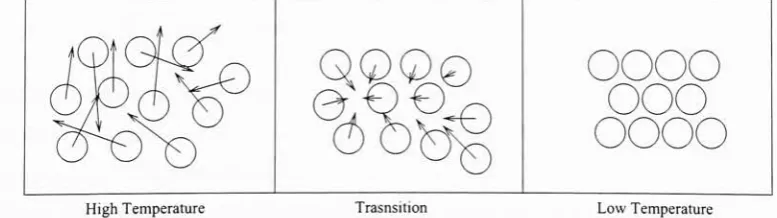
ismodeled afterthecooling ofmetal andthe behavior its molecules exhibit [1]. The focus ofthis work is to
analyze, optimize andacceleratethe Simulated
Annealing
heuristic withrespecttoitsuseimplementing
aplacement algorithm.This document is organizedas
follows;
Chapter 2 provides a motivationfor this workby
defining
itsplaceincurrentIC designflowsandexploringprior methods ofacceleratingplacement heuristics. Chapter3 provides thebackgroundof electronic design automation and IC design flow. Chapter 4 describes in depth and compares algorithms which can be usedforplacement. Chapter 5provides an analyticaldescriptionofthe SimulatedAnneal
ing
algorithm and previousresearchlooking
to improve its speed as a placementheuristic. Chapter 6 describes thesoftware implementationof aplacementtoolusedto characterizethe
timing
and analyze the critical path ofthe SimulatedAnnealing
algorithm. Chapter7 describes the hardware model generated using observations from the software imple
mentation. Chapter 8 gives the analytical process used to validate the hardware model's increase in performance. Chapter 9 details the results ofthe investigation while Chapter 10 states conclusionsdrawnfromtheinvestigationresults and provides futuredirectionfor
Chapter 2
Motivation
Itwould be difficult to arguethat anytechnique or method allowingfor adecrease in the developmenttime of aproductwouldnotbe desirable. This isespeciallytruefortheelec
tronics
industry
whichhasno foreseeableslowdown in innovationanddevelopment [35].Many
goods currently ship with IC devices providing specialized capabilities which are subject to a process that may be the critical path in the product development cycle. Toallowfurthergrowthinthecomplexityofthesedeviceswithout
imposing
restrictivedevel opmenttime overhead, accelerated methods atthecore ofthedesignflowshouldbesought[41].
As the gate count increases (in the above mentioned
devices)
so does the associateddevelopmenttime intermsofcomputationalrequirements. Computeraideddesign
(CAD)
of electronicdevicesand
targeting
themtophysicalfabrication(commonly
knownasElec tronic Design Automation(EDA)
and Physical Design Automation(PDA),
respectively)hasreducedthis time toa great extentbut improvement isrequired asdesignsgrow. Current
EDAandPDAtoolsautomatically satisfythevarious requirementsparticularto fabrication
processes while optimizingthedesignwherepossible (Mentor Graphics Design
Architect,
Mach TA and Calibre[24];
SynopsisGalaxy,
DesignWare andDiscovery
[39];
CadenceEncounter [10]). The placement process is compute intensive
[30] [36]
and represents asignificantamount oftime inthedesign flow.Aswithanyofthe stepsinthedesign
flow,
itthisstepwithin adevelopmentpath. Simulated
Annealing
[21]
isaverycommon algorithmusedtoimplementa placementtool
[2] [32] [33]
[40],
acceleratingthisalgorithmtherefore has beenthe center ofmanystudies[11]
[14] [18]
[23].Priorwork inthisfield has
firstly
focused onimproving
the SimulatedAnnealing
algorithmthroughanalyzingandmodifyingtheperturbationtypesand costfunctions
[14] [18]
[19]
[28]. Otherworkhas lookedto parallel implementation ofthe SimulatedAnnealing
algorithm purely in software to produce a speedup
[1]
[11]. The serial nature ofthe al gorithm does notdirectly
lend itselfto this approach thoughparallel implementationhasbeen showntobe successful
[8]
[23]. Otherapproachesofspeeding upthe Simulated Annealing algorithmhave focusedonhybrid implementations usingother searchmethods as
an augmentation
[18]
[20]. Hardware implementations have lookedtospecializeddataandprocessingstructures designedto be implemented in largematrices of executionelements onFPGAs[16][41].
Analyzing
the above prior work, it seems a hardware accelerated parallel processingapproach would have the ability to provide a substantial speedup.
Taking
direction from[8]
[11] [23]
and[41],
thiswork seekstofirstcharacterizethepure software placementtoolusing SAasitscoreheuristicto
identify
thecritical pathinthedata flow.Having
thisinfor mation,atailoreddatapathcanbe developedwhichwould provide some amount ofspeedupoverthesoftwaretool.
Considering
hardwareinterfacerequirements(memory
access,data structures, etc.) italso seemsfeasiblethattheparallel operationofmultiple identicaldatap
athswould producenear-linear speedupstoa point.
Applying
knowledgeofthebehavioroftheSAalgorithmwhen appliedtoplacement also provides novel approachestoahardware
Chapter 3
Background
3.1
IC Design Flow
Implementing
an electronicdesign in anintegrated circuit isby
no means atrivial task, anumber ofsteps occurbetween theconception oftheidea to the
delivery
ofthepackagedIC. Eachofthe steps inthedesignprocess are
highly
correlatedwithothers[30];
the process is usually not executed linearly. Figure 3.1 onlygives an overview ofthe IC design
flow steps. This figure is very simplified and only gives a general outline ofthe entire
Concept 1
DesignEntry
Synthesis
Placement &Routing 1
I
Physical Verification& Simulation
Fabrication
i
Review/ Validation/
[image:21.542.66.465.409.611.2]Testing
Figure 3.1: SimpleIC Design Flow
processaseach stepcontains severalunderlying steps. Asshown, theprocessmayreverse
Ofthe
following
steps, this thesis focuses onplacement. Herethe components ofthephysical designare arrangedinanattemptto producean optimizedlayout. Allother steps
areoutsidethescope ofthisworkbutareimportantin that together
they
definea semiconductor design flow.
3.1.1
Concept
-Research &
Development
The initial phase ofdesign involves the analysis ofthe original
idea,
refinement and research. Some initial steps areto determine usefulness, profitability,
feasibility,
whichtarget
technology
isused, andoverall project goals/requirements.Any
ofthe steps herewillimpact therest ofthe process, an example ofthis wouldbe the target technology. Ifhigh
performance and volume isa projectgoal, application specific IC
(ASIC)
design may betargeted whereas ifcost is a
limiting
factororthe design is to be produced in small volumesorforprototyping, lessexpensive standard cell orFPGAtechniquesmay beutilized.
Each decision here leads the project down different design
flows,
this must be carefullyconsidered inthis step.
3.1.2
Concept
-High Level Design
Here theoverall system architecture is definedand subsystems appear whichmay also be
further broken down into smaller components. The high level designistaken fromthe re
sultsofthepreviousstepand representedin modelingtools. Atthis point,eitherproprietary
ortarget
technology
vendor suppliedlibraries may be utilizedtoreduce duplicate designeffort as subsystems ofthe design may be readily available in these libraries as common
components.
Early
insights to optimizations can be discovered in this step such as data3.1.3
Design
Entry
This step begins the use ofEDA CAD tools and generates the logical representation of
the design. Two traditional types ofdesign entries are
typically
used, schematic captureand text based modeling languages with the latter
being
more popular for large designs.Schematic capture involves using a GUI to represent components and connections. The
designercreates adiagram todefinea system inwhichthe tool thencreates an intermedi
ate representationto be passed on to the next step.
Modeling
languages offerportabilityand selfdocumentationwhereinhardwaredesignsarerepresentedthrough theuseofsource
code. Two verycommonlanguagesareVHDL
[13]
andVerilog
HDL[12],
thesearewidelyused todefine hardwaresystems andtosimulate adesign before
being
mapped toatargettechnology. Others languages such as SystemC
[26]
lookto fill in the design flow gapsthat the two aforementioned languages leave open
by
not allowing overall systems to bemodeledingreatdetail.
Many
IDEs allow forboththe concurrent use of schematic entryand a modeling language in order to leverage the strengths ofboth methods (the high-level design can be
viewed inschematics andthe low-level components can be viewed in HDL).
Using
sucha tool allows for any changes in one method to update the other, maintaining coherency
across all views.
A designercan findoptimizations inthisstepthrough intelligentconstruction; a good
designerwill produceefficient, correct source code. Sometoolsused inthisstep are Men
torGraphics DesignArchitect
[24],
OrCAD PSpice[10]
andXilinx IDE(IntegratedDesignEnvironment) [42],
MentorGraphicsModelSim[24]
andAldec Active-HDL[5]
formodellanguageand/orschematic capturedevelopmentand simulation.
3.1.4
Synthesis
The designs entered in the previous step are now translated into
library
or custom comsize,shape, connection ports, and electrical characteristics. Thisisthefirststep inplacing
thedesignontothe targetsemiconductordie.
Eachcomponenthasportswhichservetomovesignalstoandfroman exterior connec
tionwhile groups of ports usuallyfromdifferent components may be connected together
to formnets. Itistheunique combination of components and connections whichgives one
design differentcharacteristicsfromanother.
Thechoice of
technology
usedgreatly influencesthisstep. IfanFPGAor standard celllibrary
is used, the designer mayuse atool toconvertthedesign into itsphysical form inwhich a componentlist and a netlistwill be generatedrepresenting the project in circuit
form. Iffull customASIC
technology
ischosen,anotherdesignerwill havetocreate components from the output oftheprevious step either from scratch or from a generic form
component. Some tools used here are Mentor Graphics' Design Compiler
[24]
and Ca dence's BuildGates [10]. AtthispointtheCADtoolsinuse move fromEDAtoPDAasthelogicalrepresentation ofthedesigniscomplete, furtherstepsdealwithapplyingthelogical
designto thephysicalprocesschosenintheconcept stages.
3.1.5
Placement
&
Routing
The components from the previous step are physically applied to the floor ofthe target
semiconductor die and the physical design begins to take shape. Here the placement of
each component generatedintheprevious stepwithrespectto everyothercomponentbe
comesimportant inordertominimizewiring delaysand congestion as well astominimize the target die size. Asthe focus ofthis work involves algorithms atthecore ofthis step,
more about placement willbe expanded uponlater.
Routing (instantiating
theconnectionsdefined
by
all nets onthe semiconductordie)
isof obvious concern as again wire lengthsshouldbe optimizedto improve performance. Mostdesigns are automatically placed and
routedforanyprojectof appreciable size. Directmanipulation
by
thedesigner issometimeswarranted but this is limited to small areas which require attention.
Efficiently
routing aPlacementandrouting may beperformedas two independent sub-steps or as a single integrated step. Performed as independent sub-steps, routing requirements must be con
sidered inthe placementstepasto providea routable design. The possibility of
having
to partiallyre-placethedesignexistsasit ispossiblethatsome aspect oftheinitialplacementwill create problems inrouting. The integratedplace and route step may possibly suffer fromunacceptably
long
runtimes as thesearch spacecreatedby
combining both steps ismuch largerthaneither step
by
itself. With current semiconductorprocesses offering fullrouting overthe components, where all interconnectionsexist above the transistor
layers,
independenceofthe two stepsbecomesmore reasonable.3.1.6
Physical
Verification
&
Simulation
Atthisstage aphysical representation oftheprojectis complete andall
timing
andelectrical characteristics ofthesystem canbe known allowing foran accurate simulationto take
place. This is known as post-place and route simulation and makes use ofparasitics ex
tractionwhichusesthegeometries of eachtransistor to
fully
specifyavery detailedmodel. Previoussimulations could not account forthe thesevalues (duetobeing
specifictophys ical construction) and were eitherignoredor estimated. Herethe system canbe measuredtoensure thephysical designwill meet criteria setforth intheprecedingstages.
Now
having
the physical characteristics ofthe target, post layout verification such as designrule checks and layoutversus schematic canbeperformedtomake surethe layout doesnot violateany fabricationrulesandbehavesasthedesignersintend,
respectfully.Any
mistakes here will
likely
sendtheproject back to the place and route stage orworse, thesynthesis stage ifa major fault is discovered. It is possible that the fundamental design would require modification at whichpoint there is no choice but to re-designaround the
problemandre-enterthecorrectioninthelogicalrepresentation. This obviouslygivesthat care shouldbe takenup to thispoint toensure correctness. Ifthedesign passes alltests it
3.1.7
Fabrication
Ifthedesign istargeted toan
ASIC,
thephysically definedproject iscreatedin a semiconductor
foundry
first as whole wafersthen individual dies andfinally
packaged dies readyfor use. In ordertoefficientlyproduceICsabuilt in selftestcanbe included inthedesign
toallow dies tobe testedbefore packaging. Inthis way ifadie fails its selftestitcanbe
discarded beforepackaging,savingtimeand money. IfanFPGAisthetargetofthe
design,
theFPGA isprogrammedusingthebitstreamgenerated
by
thedesignsuitetargeted towardtheparticular FPGA used.
Typically,
the manufacturerofthe FPGAprovides a softwarepackage to take a design from a concept to the
finished,
programmed FPGA without relianceon
third-party
tools,thoughthird-party
suites existthatreplacethisfunctionality
[5].Thefinishedproductisthenmarketed and sold orincluded inalargerproject
depending
onitspurpose.
3.2
Electronic Design Automation
Electronic Design Automation is aCAD
technology
aimed atmanaging therequirementsofworking with designs targeted to work inside of electronic technologies (custom
IC,
standardcell,FPGA). The termEDA is usuallyan umbrellatermappliedtoall CAD tech nologies usedtomanagedesigns from ideas to silicon;EDAapplies toallCADtoolsused
beforeapplicationto thephysical process and physicaldesignautomation
(PDA),
discussedbelow,
involvesallCAD toolsusedto manageadesignafterthispoint.EDAiswidelyemployedas a methodtoensurethat a group'sintellectual property
(IP)
is properly utilized
by
allowing modularizationofdesigns and creation ofproprietary libraries. Furthermoreand more
importantly,
EDAtoolsallowforreuse ofpreviouslycreatedIP,
reducing duplicate effort. Thisorganizational functionofEDAtools is notits primaryfocus;
EDA tools allow oneto easily navigate overwhelminglylarge designs with relativeease. Designs have grown in size both insubsystemhierarchies and puretransistor count
revelation,in 1965 Intelco-founderGordon MoorestatedthatICtransistorcount will dou
ble everytwo years. In 1971 the Intel 4004 hadatransistor count of
2,300,
by
1982withthe Intel286 the counthadrisentoover 130,000. Knownas Moore's
Law,
this predictionhas held trueandisforeseentodoso[35].
EDA's primary purpose is to provide a method of
translating
a design inputdescrip
tion to a logic
description, i.e.,
combinations ofbasic logic functions such asAND, OR,
XOR. As previously mentioned, the input type could be an integrated development en
vironment
(IDE)
based schematic capture where a design is"drawn"
in terms of visual
elements or atextbasedlanguagesuchasVHDL. The EDApackagewilltake theseinputs
and create generic logicaldescriptionswhichmaybe optimizedusing librarieseitherpre
viously created and archived
by
developers or providedby
the targettechnology
supplier.The strength ofEDA CAD
technology
isbeing
ableto simplyrepresent, navigate andtest largedesigns. EDA toolsprovidethe intelligence tooptimize designs withpreviously
and specifically developed components. This savesduplicate development time allowing
a group to build upon previous work and provides superior implementations of systems
without requiring intimate knowledge ofthe target technology, optimal logical function
implementationsor excessiveinteractionwiththedesigner.
3.2.1
Logical Description
The logical descriptionrepresentsthefirststepinsideanEDA CADtool toward therealiza
tionof adesignas a
fully
functional electronicdevice.Taking
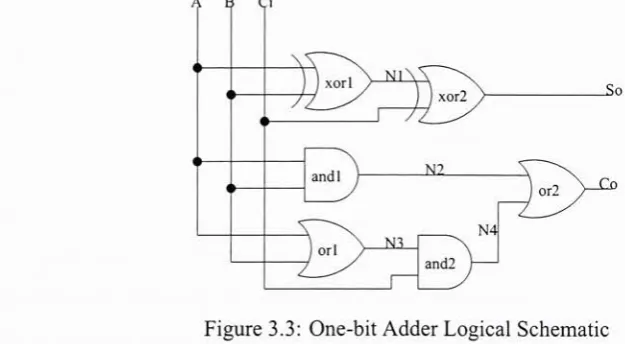
asaverysmallexamplethegeneration ofa one-bitfulladder one can showthe translationfrominputtologic
(usually
the full adder is an atomic elementof an electronicdesign but for this example it canbe
decomposed). From
fundamentals,
a one-bitfulladderisgiven asS0
=AeBCl
(3.1)
C0
= ({A *B)
+ ((A+D)
*CA
(3.2)
where
A,
B andCl
representthe adder's inputs andS0
andC0
represent the adder's sum output andcarryoutput,respectively.Having
its behaviordefined,
the design must be entered using one ofthe aforementioned methods; the core VHDL is presented in Figure 3.2 while a schematic capture is given
by
Figure 3.3. The syntaxforthe VHDL statements assigns the logic value oftheSo <= A xor B xor Ci;
Co <= ( (A and B) or ( (A or B) and Ci) ) ;
Figure 3.2: One-bit Adder Example VHDL Description
functionontherighthandside ofthe signalassignmentoperator(left arrow)to the output signal onthe left. AVHDLcompiler willthenanalyzethefilecontainingthese statements
and assemblealogical descriptionwhich canbevisualized
by
Figure3.3 whichalsowould be theinputof a schematic captureEDAtool.The EDAtoolsnow
having
thelogicalrepresentation ofthedesigncandeterminehowA 3 Ci
Figure3.3: One-bitAdderLogical Schematic
the system willact given certain
inputs,
inotherwords, the design canbe testedand examined for correctbehavior.
Usually,
this isthe firsttime the design istested with actualinputs and usuallybegins at the module level suchthat given known
interfaces,
individual designers can
independently
create modulesthatwill produce aworking system after [image:28.542.68.381.370.542.2]testbenchis generatedthatcontains testinputswithknownoutputs suchthatfastgo/no-go
tests canbe executed
during
development reducing the code/test/debugcycle's time. Forsomething as simple astheone-bitadder, anexhaustive testsetwouldbe usedtocheckall
possible combinations ofinputswhereasfor developmentpurposesina muchlarger design
alimitedtest setwouldbeusedforspotchecks
during
development. Alarger,
more complete testwould thenbe executedtoensurethat themodule willcorrectly function before
integration intothesystem.
Thebasic
building
blockusedto implement a functionwithin a designis known as alogicgate;withintheexamplefigurexor,and,and or are allinstancesof gates whichim
plementbasic logic functions. Theelementsinthisexamplecan alsobecalledcomponents,
a structure which implements some amountoffunctionality. Inthis casethe components
implementbasic
functionality,
thesemay implementmorecomplexfunctionsandit is uptothe designerofthe
library
todefinetheirgranularity. In synthesizing anarbitrary functionit may bemore efficienttoimplementa multiplexer-based
look-up
table(LUT)
ratherthanpure logic as shownhere. A synthesis tool will perform forwardand reverse elimination
in order to determine this; it's operating
theory
is outside the scope ofthis thesis. Herethe tool traverses the
boundary
between logicaland structuraldescriptions in mappingthelogic to components. It is
likely
thatunless an optimizedlibrary
component existsfortheexample one-bitadder and
depending
onthelevelofoptimization,itwouldbeinstantiatedin aLUT.
Tobedefinedasacomponent, interconnectionsmustbeable tobe madeto/fromother
components. To specifythepoints wheretheseconnectionsare made ports are used. Aport
is,
as its nameimplies,
a path which passes fromoutsidethe componentto the functionalelements inside. Aportmayhavepropertieswhichspecifythedirectionofthe logicaldata
flow inordertoallow anEDAtooltodeterminea component isused correctly. The inter
connections which aremade between ports of components are known as nets.
Typically,
anetonly connects toone port on a componentandbetweenalimitednumber of compo
nents, but may
theoretically
connectanynumber of nets ofanynumber ofcomponents.The electrical properties ofthe target
technology
limit the number of input ports anoutputport can drive. This value is known as fan-out.
Conversely,
there are real-worldlimitationsonthenumber of outputs one inputcansupport, this isnotusuallyencountered
as multiple drivers ofan input are avoided (or at least advised against
during
EDAprocessing). Thisvalue isknownasfan-inand
is,
along withfan-out,
calculatedforeach netand verified nottoexceed limitsasdefined
by
the target technology. Intheexampleabove,the nets can be identified as NI, N2, N3, N4, A, B, Ci, So and Co, the inputnets A and
B experience a fan-outofthree each, the input net Ci experiences a fan-out oftwo and
all internal nets experience a fanout of one. The output nets So and Co will experience fan-outs determined
by
the full adder's placein alarger design. Aswith functionto componentmapping, a synthesistoolwill alsoconsider these
loading
values when selectingaparticularimplementation. It is possiblethat a fasterorsmallerimplementation mayvio
late a
loading
constraint which would thenrequirebuffer(s)
toremedy. This solutionmayincrease a signal's
latency (having
to passthrough the additionalbuffer(s))
thereby
possibly decreasing
the maximumoperating speed.Selecting
an implementationwhich is lessefficientbut acceptable intermsofsatisfying
loading
constraintsmaybeabettersolution.Since noadditional buffers arerequired, signal
latency
may bereducedandthemaximumoperatingspeed may be higherthanthemore efficient implementation. Thesynthesistool
takes thisintoaccount when
determining
whichparticular components are usedinfunctionmapping.
Thecollectionofcomponentsand interconnections isknownas adesign's netlist, this
is unique to each design and subsequently defines its structure and behavior.
However,
differentnetlistsmay definethesamebehaviorthroughadifferentstructure, this isthefun
damentalprincipleofoptimization,discussed below.
Having
translatedthe one-bit adderinto a combinatoriallogicfunction,
the EDAtoolcanthenexamine the design in orderto optimize itwith pre-defined and veryefficient li
brary
implementations. Although a one-bit fulladder canbe enteredinthisfashion,
mosthighly
optimizedimplementationsthatrun much fasterthan thestraightforwarddefinition.3.2.2
Structural
Description
Having
the logicaldescriptionwhich describesthe design purelyas afunction ofinputtooutput
behavior,
an EDAtoolcanthenperformsynthesistogenerate alistof componentsand connections which implements the desired logical behavior known as the structural
description. Fromtheone-bit adder exampleabove,using fundamentalgatesthebehavior
wouldthen be implementedusingtwo each of
AND,
ORand exclusive-OR components.Inreality, thiswould not bethe case, to makefulluseofEDA'sabilities, one wouldallow
the CAD tool decide how to implement the full adder's logical function. The resulting
implementation wouldthen notbeour explicitdefinition inVHDLbut something defined
inatarget
library
givenforthefinaltechnology
implementation.Commonly,
atechnology
vendor will supply basic libraries for their products along with premium libraries which
mayperformbetterthan thebasiclibraries. Thebasic
library
wouldbe freeand alicensing
fee wouldbe paid for thepremium offering; the developerwouldthen have a
jump
starton development
having
components which are already optimized for the particular finaltechnology.
A designcanbeimplemented in many differentways which all producethesame
log
ical
behavior, however,
oneimplementationmaybesuperior over anotherdue torequiringlesscomponents orrunningat afasterclock speed. AswithmanyofthestepsintheICde
sign
flow,
computationalefforttoimplementationoptimizationtrade-offshavetobemade,as a function ofprocessingtimeversus component count andoperating frequency. A de
sign will
typically
havea number oftiming
constraints asafunctionofthenumber ofinputsand outputs. These constraintsgenerallyinvolvethe processingand production of signals
with respecttothe system clock(which mayrequire a minimum
frequency
as aconstraint)or other signals.
Knowing
the intended functions and organization ofthe structural description, thestatic
timing
of all paths canbe calculated and comparedagainsttherequiredconstraints. Optimizationthenproceedstosatisfyanyconstraintswhichhave beenviolated
by
the structural implementation. Once all constraints have been satisfied nofurther opti mization is requiredthe design flowcan thenproceed toapplying the structural design to thephysicalimplementation.3.3
Library
Exchange
Format/Design
Exchange
Format
The
Library
Exchange and Design Exchange Formats(LEF/DEF)
are ASCII text fileswhich are capableof
describing
alibrary
ofcomponents withthetechnology
inwhichthey
are implementedand a specificdesign,
respectively.OpenEDA,
sponsoredby
the Silicon Integration Initiative(SI2),
maintainstheLEF/DEFformatsas acommunityproject meaning
thatanyone isableto requestalicensetothe standards references and sources such as inthiswork[25]. SI2isan organization ofelectronics,EDAand semiconductortechnology
vendors committed to reducing cost andincreasing
productivitywithin integrated silicon systems. Thepurpose oftheLEF/DEF projectisto createan openstandard formatwhichtechnologies, librariesandindividual designs canbeexchangedbetweenorganizations us
ing
toolsetsfrom differentvendorswith notranslationissues. Most EDAtechnologiesuse the GDSII[10]
formattorepresentthe physicaldesignand proprietaryfile formatstorep resentlibrary
andnetlistinformation. The GDSIIformat is usedto transmit adesignto a fabricationfacility
suchthatitcanbeconstructedinthe targetphysical technology; GDSIIis
being
replacedby
theOASIS[34]
standard which offershigherdensity
and64-bitvalues. LEF/DEF seekstogive an openoptionto thesebinary,
proprietaryformats [25].3.3.1
LEF Syntax
technology,
viastointerconnect layersand components whichdescribealibrary.As stated above, the LEF file describes both the components and the
technology
inwhich a
library
isimplemented,
to this end, the LEF portionof adesign may thenbe bro ken intotwoseparatefiles. Ifthisisthe case, thetechnology
portion oftheLEFdescriptionmust be read first in ordertounderstand howthe components are constructed and if
they
violate any design rules. Itis an optionto combine bothtechnology
and componentdescriptions,
however,
just as iftwo separate files are used, thetechnology
section must be defined first. Thisallowsforareductionofredundantdataasonefilecanbeusedtocontainthe
technology
descriptionwhichmultiplelibrary
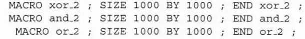
filesmayreference.Figure 3.5 givestheLEF descriptionofthe
library
usedtoimplementtheone-bit addergiven in Figure 3.3. As shown, only one type ofLEF statement is used to describe the components, the MACROstatement. Thisstatementhas manysub-statements
defining
all properties ofthe componentsuch as portlocations,
construction, electricalbehavior,
etc. The sub-statement which is usedhere is SIZE whichdefines theminimumbounding
boxwhich completelycovers all elements ofthe component. Figure 3.4 givesthe syntax of a LEF MACRO statement containingonly a SIZE sub-statement. Values ofinterest lie in
MACROmacroname ; SIZE widthBYheight ; END macroname ;
Figure3.4: LEF Syntaxfor
SIZE-only
MACRO StatementMACRO xor.2
MACRO and_2
MACRO or_2
SIZE 1000 BY 1000 ; END xor_2
SIZE 1000 BY 1000 ; END and_2
SIZE 1000 BY 1000 ; END or_2
Figure 3.5: Example LEF Definitionof aOne-BitAdder'sComponents
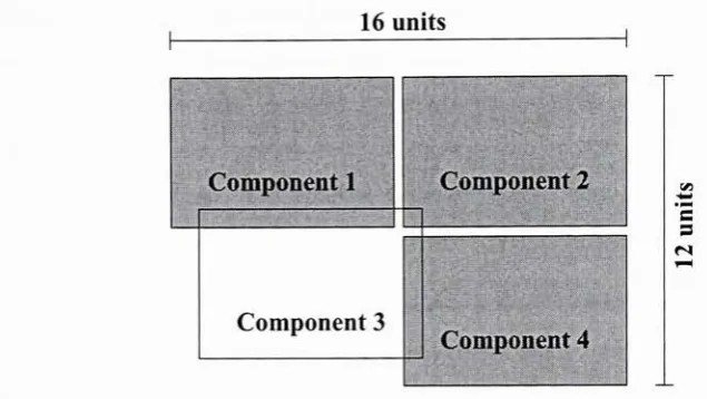
the width and heightvalues ofthe SIZEstatement which definesthe physical box which
must be placed ontothe semiconductordie. As not all components are perfectrectangles thereare constructstodefinewhich portions ofthe
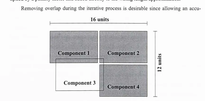
bounding
boxare notobstructedbut forthe purposesofthis work, these valuesare ignored. Itis adesignrule violationtooverlap
anyportions oftwo components,
doing
so will result in adesign which willbe unableto [image:33.542.115.421.474.514.2]correctly function. Topreventthis,these
bounding
boxesare used as theboundarieswhichdefine ifanoverlap existsbetweentwocomponentsas showninFigure 3.6.
16units
Component
1
Component2
Component 3
Component
4
Figure 3.6:
Bounding
Box Wirelength EstimationandOverlap Penalty
3.3.2
DEF Syntax
As with the case ofthe LEF
format,
it is not necessary todiscuss the DEF format in itsentirety. The DEF formatuses the information given in the LEF
file(s)
as its referencetodefineaspecific design interms ofinstancesof
library
components and interconnections.The DEF format hasthe provisionstodefine all aspects relatedto the component level of
aphysical design such as instances ofcomponents, their position, orientation, the size of
thetarget
die,
all connections betweenall instances inthedesign,
etc., andrelates closestto the focus ofthisthesis.
Specifically,
thiswork islooking
atindividualinstances,
orcomponents, and theirrelationship
toall other componentstowhichthey
are connected,knownviathe netlist. Thesample syntax ofthe DEF format is givenbelow in Figure
3.7,
the format clearly showsinstantiations of components andprovisions to declaretheir positions on the die with re
spect to their
"Southwest",
orbottom left corner. The DEF file is both the primary input [image:34.542.77.395.131.310.2]locked
by
thedesigner. Withthis,theDEFfileservesas a guidefilesuchthat theplacementalgorithm is not forcedto organize large subsections of adesign such asmemory
blocks,
arithmeticunits, etc. Also clearlyshown isthe netlistgivenby
each net's name, thecom ponent members and the respective ports connectedto the net.Having
the essentials tophysically define a
design,
instancesofcomponents, their positions andinterconnections,
one canthenproceedto
translating
alogical designgivenby
EDAtools toa physicaldeviceusing PDAtools. The example circuit, theone-bit adder, usedthroughout thisdocument D E S I GNdesignJiame ;
TECHNOLOGY techno
logy
_name ;DIEAREA ( dieJSW'.corner.coordinates
jc.y ) ( dieJVE.corner.coordinates^c.y ) ;
COMPONENTS numcomps ;
instancejiame
library
.component + FIXEDSWjc.y
j
PLACEDSWsK.y
UNPLACED ;
END COMPONENTS
NETS numnets ;
-netname ( component1port ) ( component2 port ) ... ;
END NETS
END DESIGN
Figure3.7: DEF Syntax for Simple Net
listing
is represented in a DEF file in Figure
3.8,
below. One is able to see that the design usestwo instances each ofthe three
library
components and that each instance has no initialplacementposition. Also givenare the dimensions ofthe target diewhich has an area of
36 million square units; the area required
by
the design is only six million square units (one million square units per six components). The netlist is clearly shown with all netshaving
more than one connection (the output nets have only one connection and are notpertinentinthisexample)andtheirmembercomponents.
Normally,
forafullphysicalde scription, the input/output(I/O)
pads ofthe targetdiewould alsobe defined andplaced asfixedcomponents either
by
thedesignerorthePDA tool. Theinput andoutputnetswouldthenincludethese I/Ocomponents whichwould thenbe consideredpart ofthe placement
problem.
DESIGN onebitadder
TECHNOLOGY tsmc035
DIEAREA -3000 -3000 3000 3000 )
COMPONENTS 6 ;
-xorl xor_2 + UNPLACED
-xor2 xor_2 + UNPLACED
-andl and_2 + UNPLACED
-and2 and.2 + UNPLACED
-orl or_2 + UNPLACED ;
-or2 or.2 + UNPLACED ;
END COMPONENTS
NETS 7 ;
-A ( xorl A ) ( andl A ) ( orl A
- B
( xorl B ) ( andl B ) ( orl B
- Ci
( xor2 B ) ( and2 B ) ;
-NI ( xorl Y
)
( xor2 A ) ;
-N2 ( andl Y ) ( or2 A ) ;
-N3 ( orl Y ) ( and2 A ) ;
-N4 ( and2 Y ) ( or2 B ) ;
END NETS
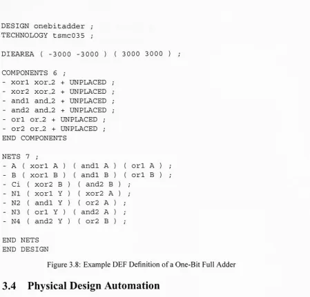
[image:36.542.66.516.54.485.2]END ]DESIGN
Figure 3.8: Example DEF Definitionof aOne-BitFull Adder
3.4
Physical Design Automation
Up
to thispointinthedevelopment flowthedesign itself has beentreatedas alogicalentity,oneperformingsomefunctionwithoutputs affected
by
itsstate and inputs. Thishas beenbroken intosubroutines and assignedtoelementsconsistingofcombinations ofbasic logic
gates. These have been instantiated incomponents which
by
themselves donot comprisea complete
design, however,
as ahierarchy
which has an organization a full descriptionis achieved. Thus the physical instantiation ofthe design
begins,
having
thelibrary
ofcomponentsandthespecificsofthesemiconductor
technology
fromtheLEFfile(s)
andthethe full listofinterconnections from the DEF
file,
the design can betreated as atangible item. With this comesthe physical manipulationofthecomponents and interconnectionsinordertoproducea usabledesign.
3.4.1
Placement
As placement will be covered in much more detail
later,
only the basic operation is describedhere. Figure 3.9 givestheinitial placementoftheexample carriedthroughout this
document,
the one-bit adder.Clearly
shown arethe six componentscomprisingthe example design. Inthis example, in order to reduce the interconnection length ofthis design
it is necessarytoplace thecomponentsas close togetheras possible. Ingeneralthere are
other considerations that may make ultra-compact placements undesirable (for example, power
density
orwiring congestion), here for simplicity andclarity,they
are not considered. Figure 3.10 givesthedesign after placementhasoccurred,
by
comparingto thepre-andl and2
xorl or2
Figure 3.9: One-bit Adder InitialRandomPlacement
vious placementonecanseethat thecomponents are placednearoptimallywith respectto
interconnectwire
length;
the software SimulatedAnnealing
algorithm(presented inChap
ter
6)
could notfindthe bestpositions forcomponents xor2 and and2. Anothernotablefeature is that there is no overlap between any ofthe components, a strong requirement
for adesirableplacement. Ifone wereto ignoreoverlap
during
placement, the algorithmwould undoubtedly find thenaive solution inwhich all components are placed on
top
ofeachother. Onereasonthat theoptimal placementwasnotdiscovered isthat thedieareais
muchlargerthan thedesignrequires, unnecessarily
increasing
thesearch space.In this example with a die size of 8000
by
8000 units and each component 1000by
1000units insize,Equation4.3 canbeusedtofindthesize ofthe search space(placement
pointstaken to the power ofthenumber of components). Giventhere are six components
which mustbeplaced, the total number of solutionsis 1.38 x 1046.
Reducing
thediewidthandheight
by
halfbringsthesearchspacedownto5.3 x IO41possible solutions while stillallowingroomfortheentiredesignwithoutoverlap.
Clearly,
enormous search spaces existforeventhesimplest of placement problems.
Asthe placement algorithm performs an actionthatis recorded, the DEFfile is
mod-xorl orl andl
or2
xor2 and2
Figure 3.10: One-bit Adder Final Placement
ified to reflectthe newpositions ofthecomponents onthe die. The
following
componentstatementsnowreplace thestatements intheinitial filegiven inFigure 3.8.
Here,
thecoor
-xorl xor_2 + PLACED ( 0 1000 ) ;
-xor2 xor_2 + PLACED ( -50 -50 ) ;
-andl and_2 + PLACED ( 2000 1000 ) ;
-and2 and_2 + PLACED ( 1000 -50 ) ;
-orl or.2 + PLACED ( 1000 1000 ) ;
-or2 or_2 + PLACED ( 2 000 0 ) ;
Figure 3.1 1: Example DEF Definitionof aOne-Bit Full Adder
keyword PLACEDwhich indicates it has been
intentionally
placedinthatlocation butmaybemoved
by
handor algorithm. Aftertheplacementstepthe design's layout isthencomplete with respecttoall
components'
positions, theinterconnectionsmust nowberouted.
3.4.2
Routing
Routing
isthePDA step thatgeneratesthephysical interconnectionsbetweencomponentsgiven
by
the netlistintheDEFfileandtheplacementfromthelaststep,respectively. Routing,
likeallEDA/PDAsteps,has manychallengeswhichmustbeovercomeor mitigatedinordertoproduce aproperly
functioning
device. Someconsiderationswhich mustbe takenintoaccount arewiringcongestion,wirecapacitance/inductancecoupling,antennaeffects,
etc. It is
likely
that some ofthese considerationsmaybeunresolvable or unacceptable intherouting step resulting inanotherroundof placementinordertoremovetheproblem. In
this case, most ofthedesignwillremainfixed andonlytheproblem area will bemodified.
Theplacement androutingstepswill theniterateuntil a routable placementis generated.
Aftertherouting stepiscompletetheroutingtoolupdatestheDEFfilewith information
indicating
thephysicallayoutoftherouting. Thisincludesspecifyinglayersused, locationsof vias andtheshape ofthe wires
implementing
thenetlist. With this,thephysical designprocesshascometoa point wherethesystemis abletobefabricatedinthesemiconductor
technology
which for itwas originallytargeted. This israrely thefinal stepas furtherverification and
testing
isperformedtoensurethe steps ofphysically creating thedesign hasnotintroducederrorswith respectto thedevice'selectrical properties.
An
interesting
consequenceofincreasing
transistorspeedsisthatwire(signaltransmission) delays have begunto become largerthan logic delays. This givesthat the insertion
ofbuffers may result in faster circuits
[7]
in certain situations. This is important to theEDA/PDA community in that tools will have to take this into consideration
during
synthesis,placement, and routing. Ifa
long
interconnection absolutelyhastobe constructed,its
delay
may possibly be mitigated through the insertion of abuffer. The design wouldthen haveto be analyzed with this buffer in placeto determine ifthere isa net benefitto
its presence. If
included,
this additional component wouldthen have to be inserted intothe
design,
possibly afterthefirst placement attempt. Iffurther placement attemptseliminate the
long interconnect,
this buffer maythenpose a performance reduction givingthatit should be removed.
Furthermore,
placement ofthe buffer with respect to the locationontheinterconnect determines itseffectiveness, a placementtoolwould thenhaveto take
this into consideration. As logic delays continue to become less than wire
delays,
theEDA/PDA community willhave to integratethe management of performance
increasing
buffers accordingly.
3.4.3
Back Annotation
This step involvesextractingall electrical characteristics ofthefinal translated,placedand
routed design in order to allow for very precise simulation. Previous simulations could
only approximate the electrical properties ofthe entire design not
knowing
the physicalgeometries ofthe device.
Now,
having
the device and it'sphysicallayout,
the simulatorcan account for previously unknown factors which may affect the performance or even
the correctness ofthe design inorderto ensurethat the final product when packaged and
inserted into a circuit will function as originally envisioned
during
the first steps oftheIC design flow. If any problems are found here the design may be sent backto previous
steps, discussedabove, to enter modifications which will
hopefully
correcttheseproblemswithout
introducing
others. Thefinal design istranslated intoa formatwhich afabricatorChapter 4
Placement
Placementinvolves arranging components inside ofthe floorplan ofthe die orFPGA tar
geted forthe constructionofthe integratedcircuit
implementing
theoriginal design. Thiscan bethoughtof as analogoustoarranging an office'sfloorplan (target
die)
withdifferentsize offices
(components)
in order to set up the floor in the most efficient way possible.Efficiency
hasmultiple variables each ofwhich must beconsidered whendetermining
anacceptable arrangement.
Making
surethat the employees ofthe office are situated closeto others which whom
they
will have the most contact with is a definite goal,however,
making sure the office holds as many employees as possible should also be considered.
Allowing
room for walkways and other essential constructs is a restriction on both thenumberof workspaces which canbe includedandtheway
they
canbeplaced onthefloor.Thesecomparisons are
directly
applicable toplacing an integratedcircuit; boththe proximity
ofinteracting
components andthedensity
oftheirplacement areofhighimportance.Additionally,
allowingroomforstructures such as wires must alsobeconsidered while arrangingthe components,ifplacedtoo
tightly
thesewillhaveno room orthesemiconductormayoverheatthuscripplingthe circuit muchinthesameway an office with no walkways
orwhichhasemployees packed against each othercould notfunction.
Determining
aperfectplacement solutionis anNP-completeproblem[30]
givingthatforany designof considerable size
finding
acomplete solution requiresoverwhelmingcomputational effort. Foradesignwith n components, thereexists a search space ontheorder
thenumber of placement grid pointstakento thepower n[30]. Withtime to market, devel
opmenttooland other administrativeconcerns, simply allowinga machinetoexhaustively
operateontrialplacements in ordertofindan optimal solutionover a matter of months or
investing
in cutting edgehardwareto reducethe computetime to daysarenot acceptablemethods ofCADassistance. Moreelegant methods ofplacementproviding verygoodbut
not perfect solutions allow fora reductionin computing effort; the cost of a non-optimal
solutionis deemedacceptablefor itspayoffinreducedplacementtime.
The act ofplacingcomponents onto a die is an example of a combinatorial optimiza
tionproblem
[36];
thegeneralformulation is introduced here. Placement isa minimizationproblemmeaningthatone placement whichhas lowercost thananotheris moredesirable
and aplacement whichhasthe leastcost isconsideredastheoptimum. Combinatorial op
timizationmayalso exist as maximizationproblemsinwhichthehighestcostisconsidered
as the optimum. A specific problem
instance,
or a unique component set andnetlist, canbe formalizedas a pair
(S,f)
where Srepresentsthefinite set of all possible solutions, orplacements, and
/
givesthe cost functionby
which individual solutions in setS maybecomparedtoone another. Thecost functionmappingis defined as
f-.s^yt
(4.i)
whichistosaythecostfunctionproduces a real valueforindividualsolutionsfroma given
set. As stated above, placement is a minimization problem; this gives that a solution is
soughtthatsatisfies
f{iopt)<f{i),VieS
(4.2)
A maximization problem uses the formula given above with the
inequality
reversed andboth minimizationand maximizationproblems use the termoptimal to representthe best
solution in set
S,
iopt or set ofbest solutions Sopt. The globally optimum solutioni^
is either aminimal or maximal solution
depending
on theproblem type, minimization ormaximization,respectively [1].
than another
by
evaluating saidparameter(s) in awaytomeaningfully representthe solutionwith respecttoothers. Cost functionsareusuallyuniqueto theproblemsinwhich
they
are
implemented,
generally makingthecomparisonoftwo differentoptimization problemsusingthesame costfunctionmeaninglessifnotimpossible. Costs canincludeanynumber
ofparameterswhich are pertinentto
finding
an optimalsolution. Asthisdeterminesabestsolution, implementation ofthecostfunction is avery importantportionofthe combina
torial optimization problem.
Along
withactuallydetermining
theoptimal solutionusingacost
function,
finding
thefunction'srepresentationwhich willgive a specific solution fromthesearch space as an optimal cost isalso anNP-complete problem.
However,
analysis ofthe problem athand willprovide verygood guidelines as howtodefine the cost
function,
i.e.,
minimizingwirelength forplacement.4.1
Exhaustive
Search
The mosttrivialmethodthatcan beusedtofind thebestplacement solution isan exhaus
tive search
involving
computingthecost of each individualplacement inside ofthesearchspace and selecting the optimal solution(s), as stated above, an NP-complete operation.
Using
the naiveapproach, the quantityof placement solutions isproportional to thenumberofplacementpoints onthe targetdietaken to thepowerofthenumber of components.
Specifically,
thenumberof solutions isgivenby
i\\{Xpointsn
xYpointsn)
(4.3)
71=0
whereiis thenumberof components andXpointsand Ypoints are thenumber of pointsin
which component n maybeplacedinthex-axisandj^-axis,respectively. Asthismethodis
very inefficientforlarger
designs,
itisrarelyused. Fortrivialdesigns (tensofcomponents),this method will provide the best output for computing effort
invested,
guaranteeing the optimum solution. Ingeneral, thismethodisnot recommended.4.2
Generalized
Hill Climbing/Local
Search
This method is a modification ofthe exhaustive search inwhich an intermediate solution
is keptonlyif its respectivecost is more desirable than the one fromwhichitwas gener ated. Though thismethod is aderivativeof exhaustive search, it has striking resemblance toSimulated
Annealing
[1]. Theconceptof aneighborhoodstructureis introduced hereto facilitategeneration of new solutionstobecompared againsttheoriginal.Aneighborhood isthe setofsolutions created
by
moving awayfromthe current solu tionby
one "step". A step is definedinthesamemannerasthecostfunction,
dependenton which parameters are pertinentto the problem and usually independent from other problems. Foreach solutioni Sa set
St
C Sofsolutionsthatare closetoiby
onestep,St
isknownastheneighborhood ofi andanysolution
j
GS,
isknownas aneighboringsolutionto i.
The algorithmusually begins
by
generatinga randomsolution, computingits cost andgeneratinga neighborhoodfromtheinitial solution. Theneighborhoodisthensearchedfor abetter solution as compared to thatwhichthe search neighborhoodwas generatedfrom.
Ifabettersolution is
found,
anewneighborhood isgenerated fromthisandtheprocessisrepeated. Theprocesscontinuestoiterateuntil a neighborhoodisgeneratedwhichcontains noneighboringsolutions with abettercostthan the prior solution.
Here,
the algorithm only moves along the hill ifthegiven path will take it to a moredesirable solution
-lowercost inthis case. Themajordownfallsofthismethod arethatit is
highly
dependentontheinitialplacementandthatitishighly
susceptibletobeing
caught in localminima.Being
purely greedy, the algorithm will consider a local minimumto be thebestsolution whenmore desirablesolutionsmayexist which areonlyreachedthrough firstincreasing
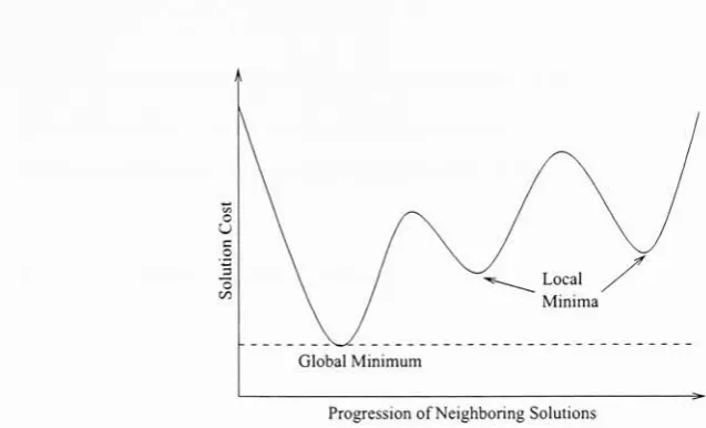
the solution's cost. Figure 4.1 displaysthis graphically. A local minimumsolutioni isdefinedas
Global Minimum
[image:45.542.63.382.58.251.2]ProgressionofNeighboringSolutions
Figure 4.1: Seriesof
Neighboring
SolutionsContaining
aLocal Minimumori isa solution whichhasalowercostthananyother solutioninitsneighborhood.
It is very possible that a poor intermediate solution will be selected such that better
solutions will neverbe encountered, this can be avoided
by
starting the algorithm withalargenumber ofinitial solutions. Asmore initial solutions areused, theprobability thata
global optimum willbe foundasymptoticallyapproaches unity [1], Giventhis, generation
and search ofinitial solutions is easilyparallelizableifindependentneighborhoods canbe
guaranteed,
i.e.,
duplicate search efforts canbeeliminated.Mixing
thismethod with othermethods, possibly as a final greedy step, may yield betterresults more efficiently than if
usedalone [36].
4.3
Min-Cut
The min-cut method is a recursive partitioningmethod which uses the principle that ifa
floorplan iscut in
half,
the fewerwiresthat it cuts, the more efficientthe placement. Themin-cut operation is performed on the sub-levels ofthefirst cut and so on until only one
component is left atthe lowest level. There are several problems with this method in its
purestform
including
loss ofinformation fromone levelto the next;however,
techniquescanbe applied allowingthe algorithm's efficiencyto be increased. With respecttoplace
mentthismethodis best usedtoquicklyconvergeon a solution used either as afinalresult
or as astartingpointforanotheralgorithm
[29]
[36].4.4
Genetic
Algorithms
Thesealgorithms take theirform fromnature and evolution, thatis to saya population is
formed,
breeding
occurs and the members who are most fit fortheir purpose survive topass goodtraits ofthe species along tothe future. In itsapplication to computing