Advanced RiSe Machines
ARM710 RISe
Processor
ARM710 Data Sheet
ARM710 RISe
Processor
ARM710 is a general purpose 32-bit microprocessor with 8kByte cache, write buffer and Memory Management Unit (MMU) combined in a single chip. The ARM710 offers high level RISC performance, yet its fully static design ensures minimal power consumption - making it ideal for portable, low cost systems.
The innovative MMU supports a conventional two-level page-table structure and a number of extensions which make it ideal for embedded control, UNIX and Object Oriented systems. This results in a high instruction throughput and impressive real-time interrupt response from a small and cost-effective chip.
r=-1
~
EJ
8kByteCache
MMU ·ARM7
• High performance RISC
Write Buffer
25 MIPS sustained @ 33 MHz (33 MIPS peak)
• Memory Management Unit (MMU)
support for virtual memory systems • 8 kByte of instruction & data cache
• Write Buffer - enhancing performance
CPU
EJ
• Fast sub microsecond interrupt response for real-time applications
• Excellent high-level language support
• Big and Little Endian operating modes
• IEEE 1149.1 Boundary Scan
• Fully static operation -low power consumption • 144 Thin Quad Flat Pack (TQFP) package
ideal for power sensitive applications
• Low power CMOS process
(1.5mA/MHz @ 3.3V)
Applications:
• Personal computer devices, eg PDAs
• High performance real time control systems
• Portable telecommunications
• Data communications equipment
• Consumer products
• Automotive
• 3 V and SV operation
r---Change Log:
Issue Date By Change
A July 93 TP Unified Frame version created.
B Sept 93 PM Corrected TOC. C July 94 EH General corrections.
© Copyright Advanced RISC Machines Ltd (ARM), 1994. All rights reserved
ARM, the ARM Powered logo, B1acldCE, and ICE brea1cer are trademarks of Advanced RISC Machines Ltd.
Neither the whole nor any part of the information contained in. or the product described in, this data sheet may be adapted or reproduced in any material form except with the prior written permission of the copyright holder.
The product described in this datasheet is subject to continuous developments and improvements. All particulars of the product and its use contained in this datasheet are given by ARM in good faith. However, all warranties implied or expressed, including but not limited to implied warranties or merchantability, or fitness for purpose, are excluded.
This datasheet is intended only to assist the reader in the use of the product. ARM Ltd shaIl not be liable for any loss or damage arising from the use of any information in this datasheet, or any error or omission in such information. or any incorrect use of the product.
Document No: ARM DDI 0024 C
Table of Contents
1.0
Introduction
1
1.1 Block Diagram 3
1.2 Functional Diagram 4
2.0
Signal Description
5
3.0
Programmer's Model
9
3.1 Register Configuration 9
3.2 Operating Mode Selection 10
3.3 Registers 11
3.4 Exceptions 14
3.5 Reset 18
4.0
Instruction Set
19
4.1 Instruction Set Summary 19
4.2 The Condition Field 20
4.3 Branch and Branch with link (B, BL) 21
4.4 Data processing 23
4.5 PSR Transfer (MRS, MSR) 30
4.6 Multiply and Multiply-Accumulate (MUL, MLA) 34
4.7 Single data transfer (LDR, STR) 36
4.8 Block Data Transfer (LDM, STM) 42
4.9 Single data swap (SWP) 49
4.10 Software interrupt (SWI) 51
4.11 Coprocessor Instructions on ARM710 53
4.12 Coprocessor data operations (CDP) 53
4.13 Coprocessor data transfers (LOC, STq 55
4.14 Coprocessor register transfers (MRC, MCR) 58
4.15 Undefined instruction 60
4.16 Instruction Set Examples 61
4.17 Instruction Speed Summary 64
5.0
Configuration
67
5.1 Internal Coprocessor Instructions 67
5.2 Registers 67
6.0
Instruction and Data Cache (lDC)
71
6.1 Cacheable Bit 71
6.2 IDC Operation 71
6.3 IDC validity 71
6.4 Read-Lock-Write 72
6.5 IDC Enable/Disable and Reset 72
7.0
Write Buffer (WB)
73
7.1 Bufferable bit 73
7.2 Write Buffer Operation 73
8.0
Coprocessors
75
9.0
Memory Management Unit (MMU)
779.1 MMU Program Accessible Registers 77
9.3 Translation Process 79
9.4 Level One Descriptor 80
9.5 Page Table Descriptor 80
9.6 Section Descriptor 80
9.7 Translating Section References 82
9.8 Level Two Descriptor 83
9.9 Translating Small Page References 84
9.10 Translating Large Page References 85
9.11 MMU Faults and CPU Aborts 86
9.12 Fault Address & Fault Status Registers (FAR & FSR) 86
9.13 Domain Access Control 88
9.14 Fault Checking Sequence 89
9.15 External Aborts 91
9.16 Interaction of the MMU, !DC and Write Buffer 91
9.17 Effect of Reset 92
10.0
Bus Interface
93
10.1 Asynchronous Mode 93
10.2 Synchronous Mode 93
10.3 ARM710 Cycle Speed 93
10.4 Cycle Types 94
10.5 Memory Access 94
10.6 Read/Write 94
lD.7 Byte/Word 94
10.8 Maximum Sequential Length 94
10.9 Memory Access Types 97
1O.lD Unbuffered Writes / Uncacheable Reads 97
10.11 Buffered Write 97
10.12 Linefetch 97
10.13 Translation fetches 98
10.14 Read - lock -write 99
10.15 Use of the nWAIT pin 100
10.16 ARM710 Cycle Type Summary 101
11.0
Boundary Scan Test Interface
103
11.1 Overview 103
11.2 Reset 104
11.3 Pullup Resistors 104
11.4 Instruction Register 104
11.5 Public Instructions 104
11.6 Test Data Registers 108
11.7 Boundary Scan Interface Signals 111
12.0
DC Parameters
115
12.1 Absolute Maximum Ratings 115
12.2 DC Operating Conditions 115
Table of Contents
13.0
AC Parameters
117
13.1 Test Conditions 117
13.2 Relationship between FCLK & MCLK in Synchronous Mode 117
13.3 Main Bus Signals 119
14.0
Physical Details
123
15.0
Pinout
125
Introduction
1.0 Introduction
ARM710 is a general purpose 32-bit microprocessor with 8kByte cache, enlarged write buffer and Memory Management Unit (MMU) combined in a single chip. The CPU within ARM710 is the ARM7. The ARM710 is software compatible with the ARM processor family and can be used with ARM support chips.
The ARM710 architecture is based on 'Reduced Instruction Set Computer' (RISC) principles, and the instruction set and related decode mechanism are greatly simplified compared with microprogrammed 'Complex Instruction Set Computers' (CISC).
The on-chip mixed data and instruction cache together with the write buffer substantially raise the average execution speed and reduce the average amount of memory bandwidth required by the processor. This allows the external memory to support additional processors or Direct Memory Access (DMA) channels with minimal performance loss.
The MMU supports a conventional two-level page-table structure and a number of extensions which make it ideal for embedded control, UNIX and Object Oriented systems.
The instruction set comprises ten basic instruction types:
• Two of these make use of the on-chip arithmetic logic unit, barrel shifter and multiplier to perform high-speed operations on the data in a bank of 31 registers, each 32 bits wide;
• Three classes of instruction control data transfer between memory and the registers, one optimised for flexibility of addressing, another for rapid context switching and the third for swapping data;
• Two instructions control the flow and privilege level of execution; and
• Three types are dedicated to the control of external coprocessors which allow the functionality of the instruction set to be extended off-chip in an open and uniform way.
The ARM instruction set is a good target for compilers of many different high-level languages. Where required for critical code segments, assembly code programming is also straightforward, unlike some RISC processors which depend on sophisticated compiler technology to manage complicated instruction interdependencies.
The memory interface has been designed to allow the performance potential to be realised without incurring high costs in the memory system. Speed-critical control signals are pipelined to allow system control functions to be implemented in standard low-power logic, and these control signals permit the exploitation of paged mode access offered by industry standard DRAMs.
ARM710 is a fully static part and has been designed to minimise its power requirements. This makes it ideal for portable applications where both these features are essential.
Datasheet Notation:
Ox
BOLD
binary
- marks a Hexadecimal quantity
- external signals are shown in bold capital letters
ARM710 is a variant of the ARM700, differing from that device in the following respects:
• no external coprocessor bus interface
• dedicated chip test port added
• device packaging
ARM710 is an enhanced and updated ARM610, differing from that device in the following respects:
• cache size increased from 4kB to 8kB
• increased maximum clock frequency
• improved write buffer
Introduction
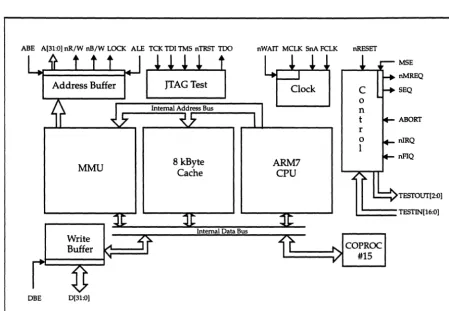
1.1 Block Diagram
ABE A[31:0] nR/W rUJ/W LOCK ALE TCK TO! TMS nTRSl' TOO nWArf MCLK SnA FCLK nRESET
'"JA'\d_dr_eS_s_B_uff_e-;r::!...---!I:;:*:;=;:;:'A;:;!:;:~=::;t=t:.I_---.~
MSEnMREQ SEQ
MMU
Write Buffer
OBE 0[31:0]
8 kByte Cache
Internal Data Bus
ARM7
CPU
ABORT
nIRQ
nFIQ
TESTOtIT[2:O]
L.!::==TESTIN[16:0]
COPROC
[image:11.620.100.550.159.470.2]L!::=~>I
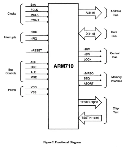
#151.2 Functional Diagram
SnA
FCLK Clocks MCLK
nWAIT
C
nlRQInterrupts nFIQ
nRESET
ABE
DBE Bus
Controls ALE MSE
C
VDD PowerVSS
A[31 :0)
J
J
nRW
]
nBW
LOCK
ARM710
nMREQ
]
SEQ
[image:12.617.81.516.161.655.2]4 ABORT
Figure 2: Functional Diagram
Address Bus
Data Bus
Control Bus
Memory Interface
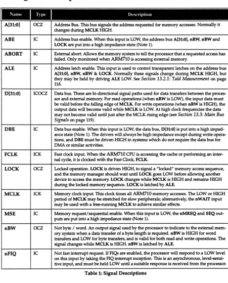
Signal Description
2.0 Signal Description
A[31:0] ABE ABORT ALE 0[31:0] DBE FCLK LOCK MCLK MSE nBW nFIQ
OCZ Address Bus. This bus signals the address requested for memory accesses. Normally it
changes during MCLK HIGH.
IC Address bus enable. When this input is LOW, the address bus A[31:0], nRW, nBW and LOCK are put into a high impedance state (Note 1).
IC Exteinal. abort. Allows the memory system to tell the processor that a requested access has failed. Only monitored when ARM710 is accessing external memory.
IC Address latch enable. This input is used to control transparent latches on the address bus A[31:0], nBW, nRW &t LOCK. Normally these signals change during MCLK HIGH, but they may be held by driving ALE LOW. See
Section
13.2.1:Tald Measurement
on page 118.ICOCZ Data bus. These are bi-directional signal paths used for data transfers between the proces-sor and exteinal. memory. For read operations (when nRW is LOW), the input data must be valid before the falling edge of MCLK. For write operations (when nRW is HIGH), the output data will become valid while MCLK is LOW. At high clock frequencies the data may not become valid until just after the MCLK rising edge (see
Section
13.3:Main Bus
Signals
on page 119).IC Data bus enable. When this input is LOW, the data bus, D[31:0] is put into a high imped-ance state (Note 1). The drivers will always be high impedance except during write opera-tions, and DBE must be driven HIGH in systems which do not require the data bus for DMA or similar activities.
ICK Fast clock input. When the ARM710 CPU is accessing the cache or performing an
inter-nal cycle, it is clocked with the Fast Oock, FCLK.
OCZ Locked operation. LOCK is driven HIGH, to signal a "locked" memory access sequence, and the memory manager should wait until LOCK goes LOW before allowing another device to access the memory. LOCK changes while MCLK is HIGH and remains HIGH during the locked memory sequence. LOCK is latched by ALE.
ICK Memory clock input. This clock times all ARM710 memory accesses. The LOW or HIGH period of MCLK may be stretched for slow peripherals; alternatively, the n W AIT input may be used with a free-running MCLK to achieve similar effects.
IC Memory request! sequential enable. When this input is LOW, the nMREQ and SEQ out-puts are put into a high impedance state (Note 1).
OCZ Not byte / word. An output signal used by the processor to indicate to the exteinal. mem-ory system when a data transfer of a byte length is required. nBW is HIGH for word transfers and LOW for byte transfers, and is valid for both read and write operations. The signal changes while MCLK is HIGH. nBW is latched by ALE.
[image:13.620.98.550.131.690.2]IC Not fast interrupt request. If FIQs are enabled, the processor will respond to a LOW level on this input by taking the FIQ interrupt exception. This is an asynchronous, level-sensi-tive input, and must be held LOW until a suitable response is received from the processor.
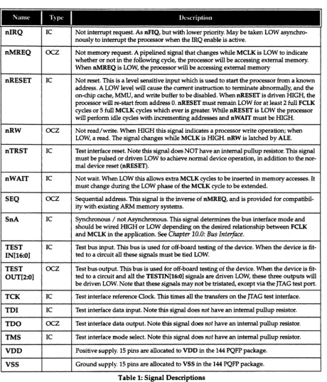
Name
I
'1'.\ peI
Description nIRQ nMREQ nRESET nRW nTRST nWAlT SEQ SnA TEST IN[16:0] TEST OUT[2:0]TCK
TDI TOO TMS VDD VSSIe
ocz
Ie
ocz
Ie
Ie
ocz
Ie
Ie
ocz
Ie
Ie
ocz
Ie
Not interrupt request. As nFIQ, but with lower priority. May be taken LOW asynchro-nously to interrupt the processor when the IRQ enable is active.
Not memory request. A pipelined signal that changes while MCLK is LOW to indicate whether or not in the following cycle, the processor will be accessing external memory. When nMREQ is LOW, the processor will be accessing external memory
Not reset. This is a level sensitive input which is used to start the processor from a known address. A LOW level will cause the current instruction to terminate abnormally, and the on-chip cache, MMU, and write buffer to be disabled. When nRESET is driven HIGH, the processor will re-start from address O. nRESET must remain LOW for at least 2 full FCLK cycles or 5 full MCLK cycles which ever is greater. While nRESET is LOW the processor will perform idle cycles with incrementing addresses and n WAIT must be HIGH. Not read/write. When HIGH this signal indicates a processor write operation; when LOW, a read. The signal changes while MCLK is HIGH. nRW is latched by ALE. Test interface reset. Note this signal does NOT have an internal pullup resistor. This signal must be pulsed or driven LOW to achieve normal device operation, in addition to the nor-mal device reset (nRESET).
Not wait. When LOW this allows extra MCLK cycles to be inserted in memory accesses. It
must change during the LOW phase of the MCLK cycle to be extended.
Sequential address. This signal is the inverse of nMREQ, and is provided for compatibil-ity with existing ARM memory systems.
Synchronous / not Asynchronous. This signal determines the bus interface mode and should be wired HIGH or LOW depending on the desired relationship between FCLK and MCLK in the application. See Chapter 10.0: Bus Interface.
Test bus input. This bus is used for off-board testing of the device. When the device is fit-ted to a circuit all these signals must be tied LOW.
Test bus output. This bus is used for off-board testing of the device. When the device is fit-ted to a circuit and all the TESTIN[16:0] signals are driven LOW, these three outputs will
be driven LOW. Note that these signals may not be tristated, except via the JTAG test port. Test interface reference Oock. This times all the transfers on the JTAG test interface. Test interface data input. Note this signal does not have an internal pullup resistor. Test interface data output. Note this signal does not have an internal pullup resistor. Test interface mode select. Note this signal does not have an internal pullup resistor. Positive supply. 15 pins are allocated to VDD in the 144 PQFP package.
[image:14.621.62.523.104.642.2]Signal Description
Notes:
1. When output pads are placed in the high impedance state for long periods, care must be taken to ensure that they do not float to an undefined logic level, as this can dissipate power, especially in the pads.
Key to Signal Types: IC - Input, CMOS threshold
OCZ - Output, CMOS levels, tri-stateable
Programmer's Model
3.0 Programmer's Model
ARM710 supports a variety of operating configurations. Some are controlled by register bits and are known as the register configurations. Others may be controlled by software and these are known as operating modes.
3.1 Register Configuration
The ARM710 processor provides 3 register configuration settings which may be changed while the processor is running and which are discussed below.
3.1.1 Big and Little Endian (the bigend bit)
The bigend bit in the Control Register sets whether the ARM710 treats words in memory as being stored in Big Endian or Little Endian format. See Chapter 5.0: Configuration for more information on the Control
Register. Memory is viewed as a linear collection of bytes numbered upwards from zero. Bytes 0 to 3 hold the first stored word, bytes 4 to 7 the second and so on.
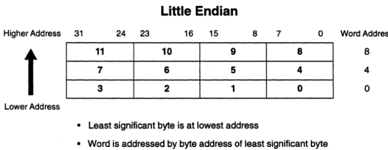
In the Little Endian scheme the lowest numbered byte in a word is considered to be the least significant byte of the word and the highest numbered byte is the most significant. Byte 0 of the memory system should be connected to data lines 7 through 0 (D[7:01) in this scheme.
Higher Address
t
I
Lower Address
Little Endian
31 24 23 16 15 8 7 0 Word Address
11 10 9 8
7 6 5 4
3 2 1
o
• Least significant byte is at lowest address
[image:17.620.122.522.368.523.2]• Word is addressed by byte address of least significant byte
Figure 3: Little Endian addresses of bytes within words
8
4
o
Big Endian
Higher Address 31 24 23 16 15 8 7 0 Word Address
t
I
8 9 10
4
5
60 1 2
11
7
3
Lower Address
• Most significant byte is at lowest address
• Word is addressed by byte address of most significant byte
Figure 4: Big Endian addresses of bytes within words
3.1.2 Configuration Bits for Backward Compatibility
8
4
a
The other two configuration bits, prog32 and data32, are used for backward compatibility with earlier ARM processors (see
16.0: Appendix - Backward Compatibility)
but should normally be set to 1. This configuration extends the address space to 32 bits, introduces major changes in the programmer's model as described below, and provides support for running existing 26 bit programs in the 32 bit environment. This mode is recommended for compatibility with future ARM processors and all new code should be written to use only the 32 bit operating modes.Because the original ARM instruction set has been modified to accommodate 32 bit operation there are certain additional restrictions which programmers must be aware of. These are indicated in the text by the words
shall
andshall not.
Reference should also be made to the ARMApplication Notes "Rules
for
ARMCode
Writers"
and"Notes for
ARMCode Writers",
available from your supplier.3.2 Operating Mode Selection
Programmer's Model
ARM710 supports six modes of operation:
(1) User mode (usr): the normal program execution state
(2) FIQ mode (fiq): designed to support a data transfer or channel process
(3) IRQ mode (irq): used for general purpose interrupt handling
(4) Supervisor mode (svc): a protected mode for the operating system
(5) Abort mode (abt): entered after a data or instruction prefetch abort
(6) Undefined mode (und): entered when an undefined instruction is executed
Mode changes may be made under software control or may be brought about by external interrupts or exception processing. Most application programs will execute in User mode. The other modes, known as privileged modes, will be entered to service interrupts or exceptions or to access protected resources.
3.3 Registers
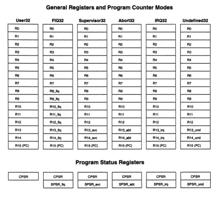
The processor has a total of 37 registers made up of 31 general 32 bit registers and 6 status registers. At any one time 16 general registers (RO to R15) and one or two status registers are visible to the programmer. The visible registers depend on the processor mode. The other registers, known as the banked registers, are switched in to support IRQ, FIQ, Supervisor, Abort and Undefined mode processing. Figure 5: Register Organisation shows how the registers are arranged, with the banked registers shaded.
In all modes 16 registers, RO to R15, are directly accessible. All registers except R15 are general purpose and may be used to hold data or address values. Register R15 holds the Program Counter (PC). When R15 is read, bits [1:0] are zero and bits [31:2] contain the Pc. A seventeenth register (the CPSR - Current Program Status Register) is also accessible. It contains condition code flags and the current mode bits and may be thought of as an extension to the Pc.
General Registers and Program Counter Modes
User32 FlQ32 Supervlsor32 Abort32 IRQ32 Undefined32
RO RO RO RO RO RO
Rl Rl Rl Rl Rl Rl
R2 R2 R2 R2 R2 R2
R3 R3 R3 R3 R3 R3
R4 R4 R4 R4 R4 R4
AS R5 AS AS R5 AS
R6 R6 R6 R6 R6 R6
R7 R7 R7 R7 R7 R7
RS ... RS_fiq RS AS RS RS
R9 R9..;.fiq R9 R9 R9 R9 Rl0 Rl0.::.flq Rl0 Rl0 Rl0 Rl0 Rll R1Uiq Rll Rll All Rll R12 Rl2.::.flq R12 R12 R12 A12 R13 R13_flq R13_svc A13J1bt ··A13.::.1rq R13;.;und R14 R14_flq A14..;.8VC A14_abt R14_irq ... R14_und R15 (PC) R15(PC) R15(PC) R15(PC) R15(PC) R15(PC)
Program Status Registers
CPSR CPSR
SPSR.:;1Iq
CPSR
~~
SPSR.;svc ...
~
~
CPSR
....
[image:20.620.71.501.122.530.2]SPSR.:;und ...
Figure 5: Register Organisation
Programmer's Model
flags
It
control
II
31 30 29 28 27 8 7 6 5 4 3 2 0
N
Z
I
c
I
VI
F M4 M3 M2 M1 MOI~
OverflowL
Mode bits Carry I Borrow I Extend FlO disableZero IROdisable
Negative I Less Than
Figure 6: Format of the Program Status Registers (PSRs)
The format of the Program Status Registers is shown in Figure 6: Format of the Program Status Registers (PSRs). The N, Z, C and V bits are the condition code flags. The condition code flags in the CPSR may be changed as a result of arithmetic and logical operations in the processor and may be tested by all instructions to determine if the instruction is to be executed.
The I and F bits are the interrupt disable bits. The I bit disables IRQ interrupts when it is set and the F bit disables FIQ interrupts when it is set. The MO, M1, M2, M3 and M4 bits (M[4:0]) are the mode bits, and these determine the mode in which the processor operates. The interpretation of the mode bits is shown in Table 2: The Mode Bits. Not all bit combinations define a valid processor mode. Only those explicitly described shall be used. The user should be aware that if any illegal value is programmed into the mode bits, M[4:0], the processor will enter an unrecoverable state. If this occurs, reset should be applied.
The bottom 28 bits of a PSR (incorporating I, F and M[4:0]) are known collectively as the control bits. These will change when an exception arises and in addition can be manipulated by software when the processor is in a privileged mode. Unused bits in the PSRs are reserved and their state shall be preserved when changing the flag or control bits. Programs shall not rely on specific values from the reserved bits when checking the PSR status, since they may read as one or zero in future processors.
M[4:0]
I
ModeI
Accessible register set10000 User PC,R14 .. RO CPSR
10001 FIQ PC, R14_fiq .. R8_fiq, R7 .. RO CPSR, SPSR_fiq 10010 IRQ PC,R14_irq .. R13_irq,R12 .. RO CPSR, SPSR_irq 10011 Supervisor PC,R14_svc .. R13_svc,R12 .. RO CPSR, SPSR_svc
10111 Abon PC,R14_abt..R13_abt,R12 .. RO CPSR, SPSR_abt 11011 Undefined PC,R14_und .. R13_und,R12 .. RO CPSR, SPSR_und
[image:21.621.114.537.515.677.2]3.4 Exceptions
Exceptions arise whenever there is a need for the normal flow of program execution to be broken, so that (for example) the processor can be diverted to handle an interrupt from a peripheral. The processor state just prior to handling the exception must be preserved so that the original program can be resumed when the exception routine has completed. Many exceptions may arise at the same time.
ARM710 handles exceptions by making use of the banked registers to save state. The old PC and CPSR contents are copied into the appropriate R14 and SPSR and the PC and mode bits in the CPSR bits are forced to a value which depends on the exception. Interrupt disable flags are set where required to prevent otherwise unmanageable nestings of exceptions. In the case of a re-entrant interrupt handler, R14 and the SPSR should be saved onto a stack in main memory before re-enabling the interrupt; when transferring the SPSR register to and from a stack, it is important to transfer the whole 32 bit value, and not just the flag or control fields. When multiple exceptions arise simultaneously, a fixed priority determines the order in which they are handled. This is listed later in Section 3.4.7: Exception Priorities on page 17.
3.4.1 FIQ
The FIQ (Fast Interrupt reQuest) exception is externally generated by taking the nFIQ input LOW. This input can except asynchronous transitions, and is delayed by one clock cycle for synchronisation before it can affect the processor execution flow. FIQ is designed to support a data transfer or channel process, and has sufficient private registers to remove the need for register saving in such applications (thus minimising the overhead of context switching). The FIQ exception may be disabled by setting the F flag in the CPSR (but note that this is not possible from User mode). If the F flag is clear, ARM710 checks for a LOW level on the output of the FIQ synchroniser at the end of each instruction.
When a FIQ is detected, ARM710:
(1) Saves the address of the next instruction to be executed plus 4 in R14_fiq; saves CPSR in SPSR_fiq
(2) Forces M[4:0]=10001 (FIQ mode) and sets the F and I bits in the CPSR
(3) Forces the PC to fetch the next instruction from address OxIC
To return normally from FIQ, use SUBS PC, R14_fiq,#4 which will restore both the PC (from R14) and the CPSR (from SPSR_fiq) and resume execution of the interrupted code.
3.4.2 IRQ
The IRQ (Interrupt ReQuest) exception is a normal interrupt caused by a LOW level on the nIRQ input. It
has a lower priority than FIQ, and is masked out when a FIQ sequence is entered. Its effect may be masked out at any time by setting the I bit in the CPSR (but note that this is not possible from User mode). If the I
Programmer's Model
(1) Saves the address of the next instruction to be executed plus 4 in R14_irq; saves CPSR in SPSR_irq
(2) Forces M[4:0]=10010 (IRQ mode) and sets the I bit in the CPSR
(3) Forces the PC to fetch the next instruction from address Ox18
To return normally from
m.Q,
use SUBS PC,R14_irq,#4 which will restore both the PC and the CPSR and resume execution of the interrupted code.3.4.3 Abort
An abort can be signalled by either the internal Memory Management Unit or from the external ABORT input. ABORT indicates that the current memory access cannot be completed. For instance, in a virtual memory system the data corresponding to the current address may have been moved out of memory onto a disc, and considerable processor activity may be required to recover the data before the access can be performed successfully. ARM710 checks for aborts during memory access cycles. When successfully aborted ARM710 will respond in one of two ways:
(1) If the abort occurred during an instruction prefetch (a Prefetch Abort), the prefetched instruction is
marked as invalid but the abort exception does not occur immediately. If the instruction is not executed, for example as a result of a branch being taken while it is in the pipeline, no abort will occur. An abort will take place if the instruction reaches the head of the pipeline and is about to be executed.
(2) If the abort occurred during a data access (a Data Abort), the action depends on the instruction type.
(a) Single data transfer instructions (LOR, STR) will write back modified base registers and the Abort handler must be aware of this.
(b) The swap instruction (SWP) is aborted as though it had not executed, though externally the read access may take place.
(c) Block data transfer instructions (LOM, STM) complete, and if write-back is set, the base is updated.
If the instruction would normally have overwritten the base with data (Le. LOM with the base in the transfer list), this overwriting is prevented. All register overwriting is prevented after the Abort is indicated, which means in particular that R15 (which is always last to be transferred) is preserved in an aborted LOM instruction.
When either a prefetch or data abort occurs, ARM710:
(1) Saves the address of the aborted instruction plus 4 (for prefetch aborts) or 8 (for data aborts) in R14_abt; saves CPSR in SPSR_abt.
(2) Forces M[4:0]=10111 (Abort mode) and sets the I bit in the CPSR
(3) Forces the PC to fetch the next instruction from either address OxOC (prefetch abort) or address Ox10 (data abort).
The abort mechanism allows a demand paged virtual memory system to be implemented when suitable
memory management software is available. The processor is allowed to generate arbitrary addresses, and when the data at an address is unavailable the MMU signals an abort. The processor traps into system software which must work out the cause of the abort, make the requested data available, and retry the aborted instruction. The application program needs no knowledge of the amount of memory available to it, nor is its state in any way affected by the abort.
Note that there are restrictions on the use of the external abort signal. See Chapter 9.0: Memory Management Unit (MMU).
3.4.4 Software interrupt
The software interrupt instruction (SWI) is used for getting into Supervisor mode, usually to request a particular supervisor function. When a SWI is executed, ARM71O:
(1) Saves the address of the SWI instruction plus 4 in R14_svc; saves CPSR in SPSR_svc
(2) Forces M[4:0]=10011 (Supervisor mode) and sets the I bit in the CPSR
(3) Forces the PC to fetch the next instruction from address Ox08
To return from a SWI, use MOVS PC,R14_svc. This will restore the PC and CPSR and return to the instruction following the SWI.
3.4.5 Undefined instruction trap
When the ARM710 comes across an instruction which it cannot handle (see Chapter 4.0: Instruction Set), it
will take the undefined instruction trap. This includes all coprocessor instructions, except MCR and MRC operations which access the internal control coprocessor.
The trap may be used for software emulation of a coprocessor in a system which does not have the coprocessor hardware, or for general purpose instruction set extension by software emulation.
When ARM710 takes the undefined instruction trap it:
(1) Saves the address of the Undefined or coprocessor instruction plus 4 in R14_und; saves CPSR in
SPSR_und.
(2) Forces M[4:0]=llOll (Undefined mode) and sets the I bit in the CPSR
(3) Forces the PC to fetch the next instruction from address Ox04
Programmer's Model
3.4.6 Vector Summary
Address
I
ExceptionI
Mode on entryOxOOOOOOOO Reset Supervisor
OXOOOOOO04 Undefined instruction Undefined
OxOOOOOOO8 Software interrupt Supervisor
OxOOOOOOOC Abort (prefetch) Abort
OxOOOOOO10 Abort (data) Abort
OxOOOOOO14 - reserved
--OxOOOOOO18 IRQ IRQ
OxOOOOOO1C FIQ FIQ
Table 3: Vector Summary
These are byte addresses, and will normally contain a branch instruction pointing to the relevant routine.
The FIQ routine might reside at OxIC onwards, and thereby avoid the need for (and execution time of) a branch instruction.
3.4.7 Exception Priorities
When multiple exceptions arise at the same time, a fixed priority system determines the order in which they will be handled:
(1) Reset (highest priority)
(2) Data abort
(3) FIQ
(4) IRQ
(5) Pre fetch abort
(6) Undefined Instruction, Software interrupt (lowest priority)
Note that not all exceptions can occur at once. Undefined instruction and software interrupt are mutually exclusive since they each correspond to particular (non-overlapping) decodings of the current instruction.
3.4.8 Interrupt Latencies
Calculating the worst case interrupt latency for the ARM710 is quite complex due to the cache, MMU and write buffer and is dependant on the configuration of the whole system. Please see Application Note -Calculating the ARM710 Interrupt Latency.
3.5 Reset
When the nRESET signal goes LOW, ARM710 abandons the executing instruction and then performs idle cycles from incrementing word addresses.
When nRESET goes mGH again, ARM710 does the following:
(1) Overwrites Rl4_svc and SPSR_svc by copying the current values of the PC and CPSR into them.
The value of the saved PC and CPSR is not defined.
(2) Forces M[4:0]=10011 (Supervisor mode) and sets the I and F bits in the CPSR.
(3) Forces the PC to fetch the next instruction from address OxOO
Instruction Set - Summary
4.0 Instruction Set
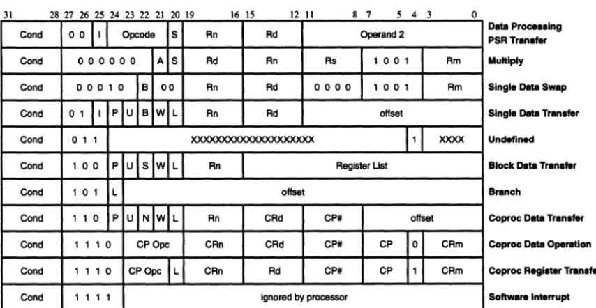
4.1 Instruction Set Summary
A summary of the ARM710 instruction set is shown in Figure 7: Instruction Set Summary.
Note: some instruction codes are not defined but do not cause the Undefined instruction trap to be taken, for instance a Multiply instruction with bit 6 changed to a 1. These instructions shall not be used, as their action may change in future ARM implementations.
31 28 27 26 25 24 23 22 21 20 19 16 15 12 II 8 7 5 4 3
Cond 00
II
Opcode S Rn Rd Operand 2 Cond o 0 000 0 A S Rd Rn Rs 1 0 0 1Cond 000 , 0 B 00 Rn Rd 0000 100 ,
Cond o 1
II
P U B W L Rn Rd offset Cond o 1 1 XXXXXXXXXXXXXXXXXXXX 1Cond ' 0 0 P U S W L Rn Register List Cond ' 0 ' L offset
Cond , , 0 P U N W L Rn CRd CPt offset Cond , , , 0 CPOpc CRn CRd CPt CP 0
Cond , , , 0 CPOpc L CRn Rd CPt CP
,
Cond,
,
, ,
ignored by processorFigure 7: Instruction Set Summary
o
Rm Rm
XXXX
CRm CRm
Data Processing PSR Transfer
Multiply
Single Data Swap
Single Data Transfer
Undefined
Block Data Transfer
Branch
Coproc Data Transfer
Coproc Data Operation
Coproc Register Transfer
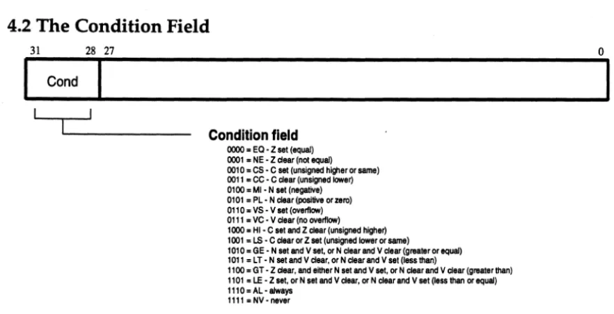
[image:27.618.110.537.243.464.2]4.2 The Condition Field
31 28 27
Cond
Condition field
0000 .. EQ • Z set (equal) 0001 • NE • Z dear (not equal)
0010 = CS • C set (unsigned hi!tler or same) 0011 "cc· C clear (unsigned kwier) 0100 .. MI· N set (negative) 0101 .. PL· N dear (positive or zero) 0110 .. VS • V set (overflow) 0111 .. VC • V clear (no overflow) 1000 • HI • C set and Z clear (unsigned hi!tler) 1001 .. LS· C clearorZ set (unsigned lower orsarne)
1010= GE· N set and V set, or N clear and V clear (graal8ror equaJ)
1011 .. LT • N set and V clear, or N dear and V set (less than)
1100 =GT· Z dear, and either N let and V set or N ciearand V clear (graaterthan) 1101 .. LE· Z set, or N set and V clear, or N ciearand V set (less than or equal) 1110 .. AL· always
[image:28.620.58.499.102.328.2]1111 =NV·never
Figure 8: Condition Codes
o
All ARM710 instructions are conditionally executed, which means that their execution mayor may not take place depending on the values of the N, 2, C and V flags in the CPSR. The condition encoding is shown in
Figure
8:Condition Codes.
If the
always
(AL) condition is specified, the instruction will be executed irrespective of the flags. Thenever
(NY) class of condition codes shall not be used as they will be redefined in future variants of the ARM architecture. If a NOP is required, MOV RO,RO should be used. The assembler treats the absence of a condition code as though
always
had been specified.Instruction Set - B, BL
4.3 Branch and Branch with link (B, BL)
The instruction is only executed if the condition is true. The various conditions are defined at the beginning of this chapter. The instruction encoding is shown in Figure 9: Branch Instructions.
Branch instructions contain a signed 2's complement 24 bit offset. This is shifted left two bits, sign extended to 32 bits, and added to the Pc. The instruction can therefore specify a branch of + / -32Mbytes. The branch offset must take account of the prefetch operation, which causes the PC to be 2 words (8 bytes) ahead of the current instruction.
31 28 27 25 24 23
o
Cond offset
L
Link bitO. Branch 1 • Branch with Link
Condition field
Figure 9: Branch Instructions
Branches beyond + / - 32Mbytes must use an offset or absolute destination which has been previously loaded into a register. In this case the PC should be manually saved in R14 if a Branch with Link type operation is required.
4.3.1 The link bit
Branch with Link (BL) writes the old PC into the link register (R14) of the current bank. The PC value written into R14 is adjusted to allow for the prefetch, and contains the address of the instruction following the branch and link instruction. Note that the CPSR is not saved with the Pc.
To return from a routine called by Branch with Link use MOV PC,R14 if the link register is still valid or LDM Rn!,{ .. PC} if the link register has been saved onto a stack pointed to by Rn.
4.3.2 Instruction Cycle Times
Branch and Branch with Link instructions take 3 instruction fetches. For more information see Section 4.17: Instruction Speed Summary on page 64.
4.3.3 Assembler syntax
B{L}{cond} <expression>
{L} is used to request the Branch with Link form of the instruction. If absent, R14 will not be affected by the instruction.
<expression> is the destination. The assembler calculates the offset.
Items in {} are optional. Items in <> must be present.
4.3.4 Examples
here BAL B
CMP BEQ
BL
ADDS BLCC
here there
Rl,#O fred
sub+ROM
Rl,#1 sub
assembles to OxEAFFFFFE (note effect of PC offset) ALways condition used as default
compare Rl with zero and branch to fred if Rl was zero otherwise continue to next instruction
call subroutine at computed address
Instruction Set - Data processing
4.4 Data processing
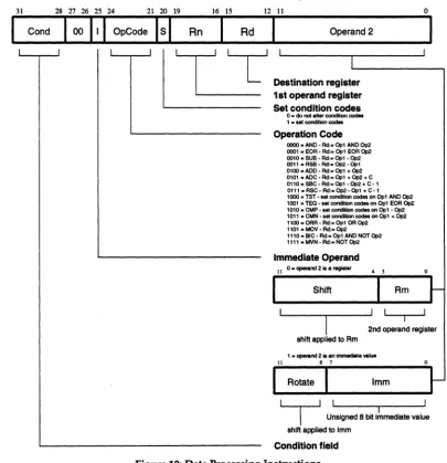
The instruction is only executed if the condition is true, defined at the beginning of this chapter. The instruction encoding is shown in Figure 10: Data Processing Instructions.
The instruction produces a result by performing a specified arithmetic or logical operation on one or two operands. The first operand is always a register (Rn). The second operand may be a shifted register (Rm) or a rotated 8 bit immediate value (lrnrn) according to the value of the I bit in the instruction. The condition codes in the CPSR may be preserved or updated as a result of this instruction, according to the value of the S bit in the instruction. Certain operations (TST, TEQ, CMP, CMN) do not write the result to Rd. They are used only to perform tests and to set the condition codes on the result and always have the S bit set. The instructions and their effects are listed in Table 4: ARM Data Processing Instructions.
31 28 27 26 25 24 21 20 19 16 15 12 II o
Cond 00
II I
OpCodeI
SI
RnI
RdI
Operand 2D
I Destination ... 's ..'-r---'
1st operand registerSet condition codes o • do not ahar condition codes
1 • oat condition codes
Operation Code
0000 • AND - Rd:. Opl AND Op2 0001 • EOR· Rd:. Opl EOR 0p2
0010. SUB - Rd:. Opl • Op2 0011 • RSB - Ad:. Op2 • Opl 0100. ADD· Rd:. Opl + Op2 0101 • ACe -Ad:= Opl + Op2 + C 0110. sec -Rd:. Opl ·Op2 + C·l 0111. RSC- Rd:a0p2-Opl + C·l 1000 • TST •• ot cond~ion codes on Opl AND Op2 1001 • TEO· sot condition codes on Qpl EOR Op2 1010 • CMP ••• , cond~ion cod .. on Opl • 0p2
1011 • CMN ·.ot cond~ codes on Opl + 0p2 1100 • ORR - Rd:. Opl OR 0p2
1101 • MOV - Rd:. Op2 1110. BIC- Rd:.Opl AND NOTOp2 1111.MVN·Rd:.NOTOp2
Immediate Operand 11 o. operand 2 is a register
Shift
I
2nd operand register shift applied to Rm1 • operand 2 ia an immediate value
8 7
Imm
I
Unsigned 8 bit Immediate value shift applied to Imm [image:31.618.122.528.251.671.2]Condition field
4.4.1 CPSR flags
The data processing operations may be classified as logical or arithmetic. The logical operations (AND,
EaR, TST, TEQ, ORR, MOV, BIC, MVN) perform the logical action on all corresponding bits of the operand or operands to produce the result. If the S bit is set (and Rd is not R15, see below) the V flag in the CPSR will be unaffected, the C flag will be set to the carry out from the barrel shifter (or preserved when the shift operation is LSL #0), the Z flag will be set if and only if the result is all zeros, and the N flag will be set to the logical value of bit 31 of the result.
Assembler
I
I
\\1' nemnllll' . OpCnde Actinn
AND 0000 operand 1 AND operand2
EOR 0001 operandI EOR operand2
SUB 0010 operand 1 - operand2
RSB 0011 operand2 - operand 1
ADD 0100 operand 1 + operand2
ADC 0101 operand 1 + operand2 + carry
SBC 0110 operand 1 - operand2 + carry - 1
RSC 0111 operand2 - operand 1
+
carry - 1TST 1000 as AND, but result is not written
TEQ 1001 as EOR, but result is not written
CMP 1010 as SUB, but result is not written
CMN 1011 as ADD, but result is not written
ORR 1100 operandI OR operand2
MOV 1101 operand2 (operandI is ignored)
BIC 1110 operandI AND NOT operand2 (Bit clear)
[image:32.618.92.487.217.583.2]MVN 1111 NOT operand2 (operandI is ignored)
Table 4: ARM Data Processing Instructions
Instruction Set - Shifts
4.4.2 Shifts
When the second operand is specified to be a shifted register, the operation of the barrel shifter is controlled by the Shift field in the instruction. This field indicates the type of shift to be performed (logical left or right, arithmetic right or rotate right). The amount by which the register should be shifted may be contained in an immediate field in the instruction, or in the bottom byte of another register (other than R15). The encoding for the different shift types is shown in Figure 11: ARM Shift Operations.
11 7 6 5 4
Shift type
00 = logical left 01 = logical right 10 = a~thmetic right 11 = rotate right
Shift amount
5 bit unsigned integer
11 8 7 6 5 4
Rs
Figure 11: ARM Shift Operations
Instruction specified shift amount
Shift type
00 = logical left 01 = logical right 10 = arithmetic right 11 = rotate right
Shift register
Shift amount specHied in bottom byte of Rs
When the shift amount is specified in the instruction, it is contained in a 5 bit field which may take any value from 0 to 31. A logical shift left (LSL) takes the contents of Rm and moves each bit by the specified amount to a more significant position. The least significant bits of the result are filled with zeros, and the high bits of Rm which do not map into the result are discarded, except that the least significant discarded bit becomes the shifter carry output which may be latched into the C bit of the CPSR when the ALU operation is in the logical class (see above). For example, the effect of LSL #5 is shown in Figure 12: Logical Shift
Left.
31 27 26 o
contents of Rm
value of operand 2
o
0 0 O· 0I
Figure 12: Logical Shift Left
Note that LSL #0 is a special case, where the shifter carry out is the old value of the CPSR C flag. The contents of Rm are used directly as the second operand.
31 S 4 0
contents of Rm
~
1 0 0 0 0 0 value of operand 2
Figure 13: Logical Shift Right
The form of the shift field which might be expected to correspond to LSR #0 is used to encode LSR #32, which has a zero result with bit 31 of Rm as the carry output. Logical shift right zero is redundant as it is the same as logical shift left zero, so the assembler will convert LSR #0 (and ASR #0 and ROR #0) into LSL #0, and allow LSR #32 to be specified.
An arithmetic shift right (ASR) is similar to logical shift right, except that the high bits are filled with bit 31 of Rm instead of zeros. This preserves the sign in 2's complement notation. For example, ASR #5 is shown in
Figure
14:Arithmetic Shift Right.
flO
S 4contents of Rm
~
~.~
I
value of operand 2I
Figure 14: Arithmetic Shift Right
The form of the shift field which might be expected to give ASR #0 is used to encode ASR #32. Bit 31 of Rm is again used as the carry output, and each bit of operand 2 is also equal to bit 31 of Rm. The result is therefore all ones or all zeros, according to the value of bit 31 of Rm.
Instruction Set - Shifts
31 5 4 0
contents of Rm
~carryout
value of operand 2
Figure 15: Rotate Right
The form of the shift field which might be expected to give ROR #0 is used to encode a special function of the barrel shifter, rotate right extended (RRX). This is a rotate right by one bit position of the 33 bit quantity formed by appending the CPSR C flag to the most significant end of the contents of Rm as shown in Figure
16: Rotate Right Extended.
31
~\
I
Register specified shift amount
o
contents of Rm
value of operand 2
Figure 16: Rotate Right Extended
Only the least significant byte of the contents of Rs is used to determine the shift amount. Rs can be any general register other than R15.
If this byte is zero, the unchanged contents of Rm will be used as the second operand, and the old value of the CPSR C flag will be passed on as the shifter carry output.
If the byte has a value between 1 and 31, the shifted result will exactly match that of an instruction specified shift with the same value and shift operation.
If the value in the byte is 32 or more, the result will be a logical extension of the shift described above:
(1) LSL by 32 has result zero, carry out equal to bit 0 of Rm.
(2) LSL by more than 32 has result zero, carry out zero.
(3) LSR by 32 has result zero, carry out equal to bit 31 of Rm.
(4) LSR by more than 32 has result zero, carry out zero.
(6) ROR by 32 has result equal to Rm, carry out equal to bit 31 of Rm.
(7) ROR by n where n is greater than 32 will give the same result and carry out as ROR by n-32; therefore repeatedly subtract 32 from n until the amount is in the range 1 to 32 and see above.
Note that the zero in bit 7 of an instruction with a register controlled shift is compulsory; a one in this bit
will cause the instruction to be a multiply or undefined instruction.
4.4.3 Immediate operand rotates
The immediate operand rotate field is a 4 bit unsigned integer which specifies a shift operation on the 8 bit immediate value. This value is zero extended to 32 bits, and then subject to a rotate right by twice the value
in the rotate field. This enables many common constants to be generated, for example all powers of 2.
4.4.4 Writing to R15
When Rd is a register other than R15, the condition code flags in the CPSR may be updated from the ALU flags as described above.
When Rd is R15 and the S flag in the instruction is not set the result of the operation is placed in R15 and the CPSR is unaffected.
When Rd is R15 and the S flag is set the result of the operation is placed in R15 and the SPSR corresponding to the current mode is moved to the CPSR. This allows state changes which atomically restore both PC and CPSR. This form of instruction shall not be used in User mode.
4.4.5 Using R15 as an operand
If R15 (the PC) is used as an operand in a data processing instruction the register is used directly.
The PC value will be the address of the instruction, plus 8 or 12 bytes due to instruction prefetching. If the shift amount is specified in the instruction, the PC will be 8 bytes ahead. If a register is used to specify the shift amount the PC will be 12 bytes ahead.
4.4.6
TEQ, TST,
CMP
&
CMN opcodes
These instructions do not write the result of their operation but do set flags in the CPSR. An assembler shall always set the S flag for these instructions even if it is not specified in the mnemonic.
The TEQP form of the instruction used in earlier processors shall not be used in the 32 bit modes, the PSR transfer operations should be used instead. If used in these modes, its effect is to move SPSR_ <mode> to CPSR if the processor is in a privileged mode and to do nothing if in User mode.
4.4.7 Instruction Cycle TlDles
Data Processing instructions vary in the number of incremental cycles taken as follows:
Normal Data Processing 1 instruction fetch
Data Processing with register specified shift
Data Processing with PC written
1 instruction fetch
+
1 internal cycleInstruction Set - TEQ, TST, CMP & CMN
Data Processing with register specified shift and PC written
3 instruction fetches and 1 internal cycle
See
Section
4.17:Instruction Speed Summary
on page 64 for more information.4.4.8 Assembler syntax
(1) MOV,MVN - single operand instructions
<opcode>{condHS} Rd,<Op2>
(2) CMP,CMN,TEQ,TST - instructions which do not produce a result.
<opcode>{cond} Rn,<Op2>
(3) AND,EOR,SUB,RSB,ADD,ADC,SBC,RSC,ORR,BIC
<opcode>{condHS} Rd,Rn,<Op2>
where <Op2> is Rm{,<shift>} or,<#expression>
{cond} - two-character condition mnemonic, see
Figure
8:Condition Codes
{S} - set condition codes if S present (implied for CMP, CMN, TEQ, TST).
Rd, Rn and Rm are expressions evaluating to a register number.
H <#expression> is used, the assembler will attempt to generate a shifted immediate 8-bit field to match the expression. H this is impossible, it will give an error.
<shift> is <shiftname> <register> or <shiftname> #expression, or RRX (rotate right one bit with extend).
<shiftname>s are: ASL, LSL, LSR, ASR, ROR. (ASL is a synonym for LSL, they assemble to the same code.)
4.4.9 Examples
ADDEQ R2,R4,RS
TEQS R4,#3
SUB R4,RS,R7,LSR R2
MOV PC,R14
MOVS PC,R14
if the Z flag is set make R2:=R4+RS
test R4 for equality with 3
(the S is in fact redundant as the assembler inserts it automatically)
logical right shift R7 by the number in the bottom byte of R2, subtract result
from RS, and put the answer into R4
return from subroutine
4.5 PSR Transfer (MRS, MSR)
The instruction is only executed if the condition is true. The various conditions are defined at the beginning of this chapter .
. The MRS and MSR instructions are formed from a subset of the Data Processing operations and are implemented using the TEQ, TST, CMN and CMP instructions without the S flag set. The encoding is
shown in
Figure
17:PSR Transfer.
These instructions allow access to the CPSR and SPSR registers. The MRS instruction allows the contents of the CPSR or SPSR_ <mode> to be moved to a general register. The MSR instruction allows the contents of a general register to be moved to the CPSR or SPSR_ <mode> register.
The MSR instruction also allows an immediate value or register contents to be transferred to the condition code flags (N,z,C and V) of CPSR or SPSR-<mode> without affecting the control bits. In this case, the top four bits of the specified register contents or 32 bit immediate value are written to the top four bits of the relevant PSR.
4.5.1 Operand restrictions
In User mode, the control bits of the CPSR are protected from change, so only the condition code flags of the CPSR can be changed. In other (privileged) modes the entire CPSR can be changed.
The SPSR register which is accessed depends on the mode at the time of execution. For example, only SPSR-fiq is accessible when the processor is in FIQ mode.
R15 shall not be specified as the source or destination register.
31
I
Instruction Set - MRS, MSR
MRS
(transfer PSR contents to a register)28 27 23 22 21
Cond
I
00010,~,
001111I
L
MSR
(transfer register contents to PSR)23 22 21
00010 1010011111
L
000000000000
Destination register Source PSR
O.CPSR
1 • SPSR_<cummt mode>
Condition field
12 11
00000000
Source register Destination PSR
O-CPSR
1 • SPSR_ <current mode>
Condition field
4 3
1
o
Rm
MSR
(transfer register contents or immediate value to PSR flag bits only)1010001111 Source operand
Destination PSR
O.CPSA
1 = SPSR_ <current mode:> Immediate Operand
11 0"" Source operand is a register
00000000
j
Source register
1 • Source operand is an immediate value 8 7
Imm
I
Unsigned 8 bit immediate value shift applied to Imm [image:39.621.111.521.95.678.2]Condition field
4.5.2 Reserved bits
Only eleven bits of the PSR are defined in ARM710 (N,Z,C,V,I,F & M[4:0]); the remaining bits (PSR[27:8,5]) are reserved for use in future versions of the processor. To ensure the maximum compatibility between ARM710 programs and future processors, the following rules should be observed:
(1) The reserved bits shall be preserved when changing the value in a PSR.
(2) Programs shall not rely on specific values from the reserved bits when checking the PSR status, since they may read as one or zero in future processors.
A read-modify-write strategy should therefore be used when altering the control bits of any PSR register;
this involves transferring the appropriate PSR register to a general register using the MRS instruction, chang4lg only the relevant bits and then transferring the modified value back to the PSR register using the MSR instruction.
e.g. The following sequence performs a mode change:
MRS
Erc
ORRMSR
RO,CPSR RO,RO,#OxlF RO,RO,#new_mode CPSR,RO
take a copy of the CPSR clear the mode bits select new mode
write back the modified CPSR
When the aim is simply to change the condition code flags in a PSR, a value can be written directly to the flag bits without disturbing the control bits. e.g. The following instruction sets the N,Z,C & V flags:
MSR CPSR_flg,#OxFOOOOOOO ; set all the flags regardless of
their previous state (does not
i affect any control bits)
No attempt shall be made to write an 8 bit immediate value into the whole PSR since such an operation cannot preserve the reserved bits.
4.5.3 Instruction Cycle Times
PSR Transfers take 1 instruction fetch. For more information see Section 4.17: Instruction Speed Summary on
page 64.
4.5.4 Assembler syntax
(1) MRS - transfer PSR contents to a register
MRS{cond} Rd,<psr>
(2) MSR - transfer register contents to PSR
MSR{cond} <psr>,Rm
(3) MSR - transfer register contents to PSR flag bits only
MSR{cond} <psrf>,Rm
Instruction Set - MRS, MSR
(4) MSR - transfer immediate value to PSR flag bits only
MSR{cond} <psrf>,<#expression>
The expression should symbolise a 32 bit value of which the most significant four bits are written to the N,Z,C & V flags respectively.
{cond} - two-character condition mnemonic, see Figure 8: Condition Codes
Rd and Rm are expressions evaluating to a register number other than R15
<psr> is CPSR, CPSR_all, SPSR or SPSR_all. (CPSR and CPSR_all are synonyms as are SPSR and SPSR_all)
Where <#expression> is used, the assembler will attempt to generate a shifted immediate 8-bit field to match the expression. If this is impossible, it will give an error.
4.5.5 Examples
In User mode the instructions behave as follows:
MSR CPSR_all,Rm CPSR[31:28] <- Rm[31:28] MSR CPSR_flg, Rm CPSR [31: 28] <- Rm[31: 28]
MSR CPSR_flg,#OxAOOOOOOO CPSR[31:28] <- OxA
(i. e. set N,Ci clear Z, V)
MRS Rd,CPSR Rd[31:0] <- CPSR[31: 0]
In privileged modes the instructions behave as follows:
MSR CPSR_all,Rm CPSR[31:0] <- Rm[31: 0] MSR CPSR_flg, Rm CPSR[31: 28] <- Rm[31: 28]
MSR CPSR_flg,#Ox50000000 CPSR[31: 28] <- Ox5
(i.e. set Z,Vi clear N,C)
MRS Rd,CPSR Rd[31:0] <- CPSR[31: 0]
MSR SPSR_all, Rm SPSR_<rnode>[31:0] <- Rm[31:0] MSR SPSR_flg, Rm SPSR_<rnode> [31:28] <- Rm[31: 28]
MSR SPSR_flg,#OxCOOOOOOO SPSR_<rnode> [31:28] <- OxC
(i. e. set N,Zi clear C,V)
4.6 Multiply and Multiply-Accumulate (MUL, MLA)
The instruction is only executed if the condition is true. The various conditions are defined at the beginning of this chapter. The instruction encoding is shown in Figure 18: Multiply Instructions.
The multiply and multiply-accumulate instructions use a 2 bit Booth's algorithm to perform integer multiplication. They give the least significant 32 bits of the product of two 32 bit operands, and may be used to synthesize higher precision multiplications.
31 28 27
I
Cond , 0 0 0 0 022 21 20 19
olAlsl
AdI
16 15 12 11 8 7
I
AnI
Aso
0 AmI I
Iu:'~~~
Operand registers Destination register Set condition code
o = do not alter condition codes 1
=
set condition codesAccumulate
o
= multiply only1 = multiply and accumulate
Condition Field
Figure 18: Multiply Instructions
o
The multiply form of the instruction gives Rd:=Rm"Rs. Rn is ignored, and should be set to zero for compatibility with possible future upgrades to the instruction set.
The multiply-accumulate form gives Rd:=Rm"Rs+Rn, which can save an explicit ADD instruction in some circumstances.
Instruction Set - MUL, MLA
4.6.1 Operand Restrictions
Due to the way multiplication was implemented, certain combinations of operand registers should be avoided. (The assembler will issue a warning if these restrictions are overlooked.)
The destination register (Rd) should not be the same as the operand register (Rm), as Rd is used to hold intermediate values and Rm is used repeatedly during multiply. A MUL will give a zero result if RM=Rd, and an MLA will give a meaningless result. R15 shall not be used as an operand or as the destination register.
All other register combinations will give correct results, and Rd, Rn and Rs may use the same register when required.
4.6.2 CPSR flags
Setting the CPSR flags is optional, and is controlled by the 5 bit in the instruction. The N (Negative) and Z (Zero) flags are set correctly on the result (N is made equal to bit 31 of the result, and Z is set if and only if
the result is zero). The C (Carry) flag is set to a meaningless value and the V (oVerflow) flag is unaffected.
4.6.3 Instruction Cycle Times
The Multiply instructions take 1 instruction fetch and m internal cycles. For more information see section 4.17 Instruction Speed Summary on page 64.
m is the number of cycles required by the multiply algorithm, which is determined by the contents of Rs. Multiplication by any number between 2"(2m-3) and 2"(2m-1J-1 takes 1S+mI cycles for
1 <m> 16. Multiplication by 0 or 1 takes 15+11 cycles, and multiplication by any number greater than or equal to 2"(29) takes 15+161 cycles. The maximum time for any multiply is thus 15+161 cycles.
4.6.4 Assembler syntax
MUL{condHS} Rd,Rm,Rs
MLA{condHS} Rd,Rm,Rs,Rn
{cond} - two-character condition mnemonic, see Figure 8: Condition Codes
{S} - set condition codes if 5 present
Rd, Rm, Rs and Rn are expressions evaluating to a register number other than R15.
4.6.5 Examples
MUL MLAEQS
Rl,R2,R3 Rl,R2,R3,R4
Rl:=R2*R3
4.7 Single data transfer (LDR, STR)
The instruction is only executed if the condition is true. The various conditions are defined at the beginning of this chapter. The instruction encoding is shown in
Figure
19:Single Data Transfer Instructions .
. The single data transfer instructions are used to load or store single bytes or words of data. The memory address used in the transfer is calculated by adding an offset to or subtracting an offset from a base register. The result of this calculation may be written back into the base register if 'auto-indexing' is required.
31 28 27 26 25 24 23 22 21 20 19 16 IS 12 II
Offset
D
r SourcalDtlstl_ roglalorBase register LoadlStore bit
0= Store to rnamary
1 • Load from rnamary Write-back bit
O. no wrn.bacI<
1 = WIlle address InIo base
BytelWord bit
0= 1I8nsIer wad quanIIIy
1 =1I8I1IIer byte quantity UplDown bit
0= daWn; subtract aIIset from base
1 • up; add oIIset to base
Pre/Post Indexing bit
o • past; add oIIset eIIer IntnsIer
1 = pre; add oIIset befara Inmoler Immediate offset
II o. oIIset is an _ _ value
Immediate offset
Unsigned 12 bit immediate offset
II h oIIsst is a ragIsIar
Shift
o
shift applied to Rm
[image:44.620.89.485.231.638.2]Condition field
Figure 19: Single Data Transfer Instructions
Instruction Set - LDR, STR
4.7.1 Offsets and auto-indexing
The offset from the base may be either a 12 bit unsigned binary immediate value in the instruction, or a second register (possibly shifted in some way). The offset may be added to (U=I) or subtracted from (U=O) the base register Rn. The offset modification may be performed either before (pre-indexed, P=I) or after (post-indexed, p=o) the base is used as the transfer address.
The W bit gives optional auto increment and decrement addressing modes. The modified base value may be written back into the base (W=I), or the old base value may be kept (W=O). In the case of post-indexed addressing, the write back bit is redundant and is always set to zero, since the old base value can be retained by setting the offset to zero. Therefore post-indexed data transfers always write back the modified base. The only use of the W bit in a post-indexed data transfer is in privileged mode code, where setting the W bit forces non-privileged mode for the transfer, allowing the operating system to generate a user address in a system where the memory management hardware makes suitable use of this hardware.
4.7.2 Shifted register offset
The 8 shift control bits are described in the data processing instructions section. However, the register specified shift amounts are not available in this instruction class. See Section 4.4.2: Shifts on page 25.
4.7.3 Bytes and words
This instruction class may be used to transfer a byte (B=I) or a word (B=O) between an ARM710 register and memory.
The action of LOR(B) and STR(B) instructions is influenced by the 3 instruction fetches. For more information see Section 4.17: Instruction Speed Summary on page 64. The two possible configurations are described below.
Little Endian Configuration
A byte load (LORB) expects the data on data bus inputs 7 through 0 if the supplied address is on a word boundary, on data bus inputs 15 through 8 if it is a word address plus one byte, and so on. The selected byte is placed in the bottom 8 bits of the destination register, and the remaining bits of the register are filled with zeros. Please see Figure 4: Big Endian addresses of bytes within words.
A byte store (STRB) repeats the bottom 8 bits of the source register four times across data bus outputs 31 through o. The external memory system should activate the appropriate byte subsystem to store the data.